- Select a language for the TTS:
- UK English Female
- UK English Male
- US English Female
- US English Male
- Australian Female
- Australian Male
- Language selected: (auto detect) - EN
Play all audios:
ABSTRACT Silicon nanowires (SiNWs) are attracting growing interest due to their unique properties and promising applications in photovoltaic devices, thermoelectric devices, lithium-ion
batteries and biotechnology. Low-cost mass production of SiNWs is essential for SiNWs-based nanotechnology commercialization. However, economic, controlled large-scale production of SiNWs
remains challenging and rarely attainable. Here, we demonstrate a facile strategy capable of low-cost, continuous-flow mass production of SiNWs on an industrial scale. The strategy relies on
substrate-enhanced metal-catalyzed electroless etching (MCEE) of silicon using dissolved oxygen in aqueous hydrofluoric acid (HF) solution as an oxidant. The distinct advantages of this
novel MCEE approach, such as simplicity, scalability and flexibility, make it an attractive alternative to conventional MCEE methods. SIMILAR CONTENT BEING VIEWED BY OTHERS CATALYST-FREE
SYNTHESIS OF SUB-5 NM SILICON NANOWIRE ARRAYS WITH MASSIVE LATTICE CONTRACTION AND WIDE BANDGAP Article Open access 20 June 2022 VERSATILELY TUNED VERTICAL SILICON NANOWIRE ARRAYS BY
CRYOGENIC REACTIVE ION ETCHING AS A LITHIUM-ION BATTERY ANODE Article Open access 05 October 2021 LOW-COST FABRICATION METHODS OF ZNO NANORODS AND THEIR PHYSICAL AND PHOTOELECTROCHEMICAL
PROPERTIES FOR OPTOELECTRONIC APPLICATIONS Article Open access 11 October 2024 INTRODUCTION Large-scale fabrication of SiNWs1,2,3,4,5,6,7 is of great importance in pursuit of exploring SiNWs
for wide-ranging technological applications8,9,10,11,12,13,14,15,16 in electronics, photonics, renewable energy and biotechnology. Despite intense efforts, mass production of SiNWs on an
industrial scale remains unattainable. SiNWs are commonly produced by chemical vapor deposition methods7 via vapor-liquid-solid (VLS) mechanism. However the VLS method can only produce SiNWs
in limited quantities. Recently, metal-catalyzed electroless etching (MCEE) of silicon17,18,19,20,21,22,23,24,25,26,27,28,29,30, also known as metal-assisted chemical etching (MACE), has
been widely used to fabricate high-aspect ratio SiNWs and other silicon nanostructures such as nanoholes due to its simplicity and low cost. The nature of MCEE of silicon in aqueous HF
solution is galvanic corrosion. In traditional well-established MCEE methods, common oxidizing agent such as hydrogen peroxide or silver nitrate is
indispensable17,18,19,20,21,22,23,24,25,26,27,28,29,30. To date, MCEE SiNWs have been widely investigated for photovoltaic device, thermoelectric device, lithium-ion battery and biological
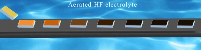
applications9,31,32,33,34,35,36,37. Here we report simple and low-cost MCEE of silicon in aerated aqueous HF solution enabling mass production of SiNWs with unprecedented ease. The process
relies on substrate-enhanced MCEE of silicon using dissolved oxygen in aqueous HF solution as a green oxidant, which is ubiquitous in nature, yet completely neglected in traditional MCEE
methods due to sluggish oxygen reduction kinetics. We demonstrate that this approach can establish continuous-flow production of SiNWs on an industrial scale, offering unparalleled
advantages over traditional approaches in terms of cost, processing time and versatility. The continuous-flow mass-production process for SiNWs is schematically shown in Fig. 1 (see Methods
for details). The production line consists of conductive graphite (or noble metal such as Ag, Au and Pt) substrates immersed in aerated aqueous HF solution, in which SiNW arrays are produced
by continuously flowing Si substrates through the aerated aqueous HF solution. RESULTS GRAPHITE SUBSTRATE-ENHANCED MCEE OF SILICON IN AERATED AQUEOUS HF SOLUTION To promote selective Si
corrosion and create high-aspect ratio SiNWs, the surfaces of the starting Si materials must be pre-patterned with noble metal catalysts such as silver or gold (silver nanoparticles, AgNPs
are used here). Otherwise, only a thin porous Si layer would be formed from bare Si wafer or powders (Fig. S1). Our experimental results show that aligned SiNWs could be created on Si wafers
of different doping types and concentrations. Figure 2a and 2b show respectively the typical cross-sectional scanning electron microscope (SEM) images of large-area vertically aligned SiNW
arrays prepared on p-type 1–10 Ω · cm Si(100) and n-type 2–3 Ω · cm Si(100) wafers after one pass (2 hours) through aerated aqueous HF solution. The SEM images clearly show that the
corrosion rate of p-Si is faster than that of n-Si under the same conditions, revealing different corrosion behaviors of p- and n-type silicon due to their distinct charge carrier
characteristics. The as-prepared SiNWs are typically 20–250 nm in diameter, while wire lengths could be simply controlled by changing corrosion time. High-resolution transmission electron
microscopic (TEM) images in Figure 2c and 2d reveal the single crystalline nature of SiNWs in Figure 2a and 2b, respectively. The images show that the axial orientations of the nanowires are
along the [100] directions, indicating the preferential anisotropic etching of <100> silicon. HR-TEM images also reveal that the surface of SiNWs from low-doped p-type 1–10 Ω · cm
Si(100) wafer is relatively smooth, while that from highly-doped p-type 0.001–0.008 Ω · cm Si(100) wafer is extremely mesoporous (Fig. S2). Note that the geometries of etched Si
nanostructures are dependent on the pattern or shape of noble metal catalysts, therefore a variety of Si nanostructures with distinct features could be fabricated by precisely predefining
the patterns of noble metal catalysts. Fig. S3 shows the typical SEM image of regular silicon nanoholes with controlled geometry and density. We evaluate the substrate-enhanced MCEE of
silicon by galvanic current measurements, which were performed in a home-made electrochemical cell. The silicon area exposed to aqueous HF solution is 1.0 cm2 and the Si/Graphite surface
area ratio is set to 1:200. Figure 3 shows the galvanic current densities as a function of time for silicon and graphite coupled together through an external wire. The galvanic current rises
sharply as the circuit is short-circuited and then levels off with time. The initial abrupt drop in corrosion current is due to the limited solubility of oxygen in aqueous HF solution. In
the presence of AgNPs, the measured current density of the p-Si/Graphite galvanic cell is considerably larger than that of n-Si/Graphite galvanic cell in the presence of AgNPs (Fig. 3a) and
nearly two orders of magnitude greater than that of p-Si/Graphite galvanic cell in the absence of AgNPs (Fig. 3b). These results are well consistent with our SEM observations. Due to direct
contact of noble metal catalysts with silicon in aqueous HF solution, the microscopic Si/AgNPs galvanic cells do not contribute to the measured corrosion current, which originates from the
macroscopic Si/Graphite galvanic cell. Assuming a constant corrosion rate, the corrosion current density from microscopic Si/AgNPs galvanic cells reaches 1.3 mA/cm2 using Faraday's law
based on the mass loss of silicon and galvanic current-time curve measured for macroscopic p-Si/Graphite galvanic cell in the presence of AgNPs. The role of dissolved oxygen in aqueous HF
solution was investigated by conducting corrosion experiment in de-aerated aqueous HF solution bubbling with high-purity nitrogen gas. In the presence of AgNPs, the steady-state current
density of the p-Si/Graphite galvanic cell in de-aerated aqueous HF solution was 0.007 mA/cm2 (Fig. 3b), which is three orders of magnitude lower than that of a similar cell in aerated
aqueous HF solution, showing silicon corrosion is completely governed by oxygen reduction reaction. NOBLE METAL SUBSTRATE-ENHANCED MCEE OF SILICON IN AERATED AQUEOUS HF SOLUTION We further
investigated noble metals (Ag, Au and Pt) substrate-enhanced MCEE of silicon in aerated aqueous HF solution for SiNWs fabrication under the same conditions. Figure 4a–c show the typical
cross-sectional SEM images of SiNW arrays prepared on p-type 1–10 Ω · cm Si(100) wafers placed on Ag, Au and Pt substrates, respectively. The etching time is 2 hours. These SEM images
clearly reveal that the length of produced SiNWs or the etching rate strongly depends on the type of used noble metal substrates and increases in the order of Ag, Au and Pt, indicating these
metal substrates show quite different catalytic activity in the cathodic oxygen reduction reaction. To investigate catalytic activities of noble metal substrates in oxygen reduction, we
carry out galvanic corrosion experiments by measuring the galvanic current of noble metal substrates coupled with silicon substrates in aerated aqueous HF solution. Figure 4d shows the
measured galvanic current densities as a function of time for silicon substrates coupled with Ag, Au and Pt substrates. It clearly reveals that the galvanic current increases in the same
order of Ag, Au and Pt, which is well consistent with SEM observations. These results imply that catalytic activities of the cathodes considerably affect oxygen reduction and accompanied
silicon etching rates in aerated aqueous HF solution. DISCUSSION The above results demonstrate that the present substrate-enhanced MCEE approach is a very simple method for preparing SiNW
arrays without needing the common toxic oxidizing agents such as silver nitrate and hydrogen peroxide. In the absence of graphite or noble metal substrates, only shallow pits, as shown in
Fig. S4, are produced on Si surface. Additionally, since only thin porous silicon is produced in the absence of noble metal catalysts, we conclude that the corrosion rate of silicon in the
presence of both graphite and noble metal catalysts is much faster than that when either one of them is used alone, revealing the strong synergistic enhancing effect of graphite and noble
metal for galvanic corrosion of silicon. An electrochemical model of the synergistic galvanic corrosion process is proposed as schematically illustrated in Fig. 5a. Due to the electrode
potential difference, a macroscopic galvanic cell between Si and graphite, accompanying by microscopic galvanic cells between Si and noble metal catalysts, is constructed when Si wafer
coated with noble metal catalysts are electrically coupled to graphite substrate in aerated aqueous HF solution. While random and stochastic microscopic galvanic cells may exist on Si
surface38, they contribute negligibly to silicon corrosion in aerated aqueous HF solution. The anodic and cathodic half-cell reactions for the substrate-enhanced MCEE of silicon are
described as follows: Briefly, the dissolved oxygen is reduced on both surfaces of graphite and noble metal catalysts, while silicon is oxidized by releasing electrons. Due to enhanced
cathodic oxygen reduction, the anodic silicon dissolution reaction is simultaneously accelerated. As current lines always follow the minimal ohmic resistance, thus the electrical current
flowing through the silicon/metal interface within the propagating pits would be very intense, resulting in highly selective pitting corrosion of silicon underneath the noble metal catalysts
and consequential formation of silicon nanostructures with considerable depth (Fig. 5b). We suggest that the macroscopic galvanic cell between Si and graphite in combination with the
microscopic galvanic cells between Si and noble metal catalysts contribute to the intense corrosion current, which is also significantly affected by the charge carrier characteristics of Si
substrates. Consequently, the corrosion rate of p-type Si is faster due to the abundant holes in p-Si, while that of n-type Si is slower due to the limited supply of holes. In conclusion, we
demonstrate for the first time the simple, continuous-flow mass production of SiNWs via substrate-enhanced MCEE of silicon using dissolved oxygen in aqueous HF solution as a green oxidant.
The distinct advantages of this novel approach such as simplicity, scalability and flexibility would make it an attractive alternative to conventional MCEE methods. Since galvanic corrosion
occurs in all semiconductor-metal and metal-metal systems, we suggest that such galvanic corrosion processes may be generally adopted to fabricate other semiconducting and metallic
nanostructures. METHODS FABRICATION OF SILICON NANOWIRES SiNWs can be prepared on different starting Si materials, including single-crystalline silicon wafer, multi-crystalline silicon
wafer, thin silicon film and silicon particles, by means of substrate-enhanced MCEE of silicon in a continuous production line consisting of graphite or noble metal (Ag, Au and Pt)
substrates immersed in aerated aqueous HF solution. To prepare high-aspect ratio SiNWs, Si materials must be pre-coated with thin noble metal (Ag, Au) particles before being placed onto
graphite or noble metal substrates immersed in aerated aqueous HF solution. Only porous silicon was prepared from clean Si materials placed on a graphite substrate immersed in aerated
aqueous HF electrolyte (10% in weight) for 10–300 minutes. All experiments were carried out at room temperature. All chemicals were purchased from Sigma–Aldrich. STRUCTURAL AND
ELECTROCHEMICAL CHARACTERIZATION The morphologies and microstructures of silicon nanostructures were investigated using a field-emission scanning electron microscope (SEM, HITACHI S-4800)
and a transmission electron microscope (TEM, JEOL JEM-2100). The galvanic corrosion current was measured in a Teflon-made electrochemical cell. The de-aerated aqueous HF electrolyte was
prepared by purging high-purity N2 through the solution for 1 hour. The electrochemical measurements were performed using a Zennium electrochemical workstation (IM6, Zahner, Germany) with
silicon as the working electrode and a graphite rod as the counter electrode. Ohmic contact was made by pasting high-purity In-Ga alloy onto the rear side of the Si wafer with 1 cm2 of the
front surface area exposed to aqueous HF solution. REFERENCES * Morales, A. M. & Lieber, C. M. A laser ablation method for the synthesis of crystalline semiconductor nanowires. Science
279, 208–211 (1998). Article ADS CAS Google Scholar * Ma, D. D. D., Lee, C. S., Au, F. C. K., Tong, S. Y. & Lee, S. T. Small diameter silicon nanowire surface. Science 299, 1874–1877
(2003). Article ADS CAS Google Scholar * Hannon, J. B., Kodambaka, S., Ross, F. M. & Tromp, R. M. The influence of the surface migration of gold on the growth of silicon nanowires.
Nature 440, 69–71 (2006). Article ADS CAS PubMed Google Scholar * Wang, Y., Schmidt, V., Senz, S. & Gösele, U. Epitaxial growth of silicon nanowires using an aluminum catalyst. Nat.
Nanotech. 1, 186–189 (2006). Article ADS CAS Google Scholar * Hochbaum, A. I., Fan, R., He, R. & Yang, P. Controlled growth of Si nanowire arrays for device integration. Nano Lett.
5, 457–60 (2005). Article ADS CAS PubMed Google Scholar * Renard, V. T. et al. Catalyst preparation for CMOS-compatible silicon nanowire synthesis. Nat. Nanotech. 4, 654–657 (2009).
Article ADS CAS Google Scholar * Schmidt, V., Wittemann, J. V., Senz, S. & Gösele, U. Silicon nanowires: a review on aspects of their growth and their electrical properties. Adv.
Mater. 21, 2681–2702 (2009). Article CAS Google Scholar * Cui, Y. & Lieber, C. M. Functional nanoscale electronic devices assembled using silicon nanowire building blocks. Science
291, 851–853 (2001). Article ADS CAS PubMed Google Scholar * Hochbaum, A. I. et al. Enhanced thermoelectric performance of rough silicon nanowires. Nature 451, 163–167 (2008). Article
ADS CAS PubMed Google Scholar * Peng, K. Q., Wang, X., Li, L., Hu, Y. & Lee, S. T. Silicon nanowires for advanced energy conversion and storage. Nano Today 8, 75–97 (2013). Article
CAS Google Scholar * Chan, C. K. et al. High-performance lithium battery anodes using silicon nanowires. Nat. Nanotech. 3, 31–35 (2008). Article ADS CAS Google Scholar * Tian, B. et
al. Coaxial silicon nanowires as solar cells and nanoelectronic power sources. Nature 449, 885–890 (2007). Article ADS CAS Google Scholar * Zheng, G., Patolsky, F., Cui, Y., Wang, W. U.
& Lieber, C. M. Multiplexed electrical detection of cancer markers with nanowire sensor arrays. Nat. Biotechnol. 23, 1294–1301 (2005). Article CAS PubMed Google Scholar * Kelzenberg,
M. D. et al. Enhanced absorption and carrier collection in Si wire arrays for photovoltaic applications. Nat. Mater. 9, 239–244 (2010). Article ADS CAS PubMed Google Scholar *
Boettcher, S. W. et al. Energy-conversion properties of vapor-liquid-solid-grown silicon wire-array photocathodes. Science 327, 185–187 (2010). Article ADS CAS PubMed Google Scholar *
Shen, X., Sun, B., Liu, D. & Lee, S. T. Hybrid heterojunction solar cell based on organic–inorganic silicon nanowire array architecture. J. Am. Chem. Soc. 133, 19408–19415 (2011).
Article CAS PubMed Google Scholar * Peng, K. Q., Yan, Y. J., Gao, S. P. & Zhu, J. Synthesis of large-area silicon nanowire arrays via self-assembling nanoelectrochemistry. Adv.
Mater. 14, 1164–1167 (2002). Article CAS Google Scholar * Li, X. & Bohn, P. W. Metal-assisted chemical etching in HF/H2O2 produces porous silicon. Appl. Phys. Lett. 77, 2572–2574
(2000). Article ADS CAS Google Scholar * Peng, K. Q. et al. Fabrication of single-crystalline silicon nanowires by scratching a silicon surface with catalytic metal particles. Adv.
Funct. Mater. 16, 387–394. (2006). Article CAS Google Scholar * Huang, Z., Fang, H. & Zhu, J. Fabrication of silicon nanowire arrays with controlled diameter, length and density. Adv.
Mater. 19, 744–748 (2007). Article CAS Google Scholar * Peng, K. Q., Lu, A. J., Zhang, R. Q. & Lee, S. T. Motility of metal nanoparticles in silicon and induced anisotropic silicon
etching. Adv. Funct. Mater. 18, 3026–3035 (2008). Article CAS Google Scholar * Choi, W. K. et al. Synthesis of silicon nanowires and nanofin arrays using interference lithography and
catalytic etching. Nano Lett. 8, 3799–3802 (2008). Article ADS CAS PubMed Google Scholar * Hochbaum, A. I., Gargas, D., Hwang, Y. J. & Yang, P. D. Single crystalline mesoporous
silicon nanowires. Nano Lett. 9, 3550–3554 (2009). Article ADS CAS PubMed Google Scholar * Peng, K. Q. et al. Uniform, axial-orientation alignment of one-dimensional single-crystal
silicon nanostructure arrays. Angew. Chem. Int. Ed. 44, 2737–2740 (2005). Article CAS Google Scholar * Huang, Z. et al. Ordered arrays of vertically aligned [110] silicon nanowires by
suppressing the crystallographically preferred etching directions. Nano Lett. 9, 2519–2525 (2009). Article ADS CAS PubMed Google Scholar * Chen, H., Wang, H., Zhang, X. H., Lee, C. S.
& Lee, S. T. Wafer-scale synthesis of single-crystal zigzag silicon nanowire arrays with controlled turning angles. Nano Lett. 10, 864–868 (2010). Article ADS CAS PubMed Google
Scholar * Huang, Z., Geyer, N., Werner, P., Boor, J. & Gösele, U. Metal-assisted chemical etching of silicon: A review. Adv. Mater. 23, 285–308 (2011). Article CAS Google Scholar *
Peng, K. Q. et al. Ordered silicon nanowire arrays via nanosphere lithography and metal-induced etching. Appl. Phys. Lett. 90, 163123 (2007). Article ADS Google Scholar * Weisse, J., Kim,
D., Lee, C. & Zheng, X. Vertical transfer of uniform silicon nanowire arrays via crack formation. Nano Lett. 11, 1300–1305 (2011). Article ADS CAS PubMed Google Scholar * Peng, K.
Q., Wang, X., Li, L., Wu, X. L. & Lee, S. T. High-performance silicon nanohole solar cells. J. Am. Chem. Soc. 132, 6872–6873 (2010). Article CAS PubMed Google Scholar * Peng, K. Q.
et al. Aligned single-crystalline Si nanowire arrays for photovoltaic applications. Small 1, 1062–1067 (2005). Article CAS PubMed Google Scholar * Garnett, E. C. & Yang, P. D.
Silicon nanowire radial p-n junction solar cells. J. Am. Chem. Soc. 130, 9224–9225 (2008). Article CAS PubMed Google Scholar * Sivakov, V. et al. Silicon nanowire-based solar cells on
glass: synthesis, optical properties and cell parameters. Nano Lett. 9, 1549–1554 (2009). Article ADS CAS PubMed Google Scholar * Huang, R., Fan, X., Shen, W. & Zhu, J.
Carbon-coated silicon nanowire array films for high-performance lithium-ion battery anodes. Appl. Phys. Lett. 95, 133119 (2009). Article ADS Google Scholar * Peng, K. Q., Wang, X. &
Lee, S. T. Gas sensing properties of single crystalline porous silicon nanowires. Appl. Phys. Lett. 95, 243112 (2009). Article ADS Google Scholar * Wang, X. T., Shi, W. S., She, G. W.
& Mu, L. X. Using Si and Ge Nanostructures as substrates for surface-enhanced Raman scattering based on photoinduced charge transfer mechanism. J. Am. Chem. Soc. 133, 16518–16523 (2011).
Article CAS PubMed Google Scholar * Chen, L. et al. Aptamer-mediated efficient capture and release of T llymphocytes on nanostructured surfaces. Adv. Mater. 23, 4376–4380 (2011).
Article CAS PubMed Google Scholar * Turner, D. R. On the mechanism of chemically etching germanium and silicon. J. Electrochem. Soc. 107, 810–816 (1960). Article CAS Google Scholar
Download references ACKNOWLEDGEMENTS We acknowledge financial support from National Natural Science Foundation of China (51072025), National Basic Research Program of China (2012CB932400),
Beijing Natural Science Foundation (2112021), The Fundamental Research Funds of the Central Universities (2012LZD02) and Fok Ying Tung Education Foundation (121047). AUTHOR INFORMATION
AUTHORS AND AFFILIATIONS * Department of Physics and Beijing Key Laboratory of Energy Conversion and Storage Materials, Beijing Normal University, Beijing, China Ya Hu, Kui-Qing Peng, Lin
Liu, Zhen Qiao & Xiao-Ling Wu * Technical Institute of Physics and Chemistry, Key Laboratory of Photochemical Conversion and Optoelectronic Materials, Chinese Academy of Sciences,
Beijing, China Xing Huang & Xiang-Min Meng * Institute of Functional Nano and Soft Materials (FUNSOM) and Collaborative Innovation Center of Suzhou Nano Science and Technology, Soochow
University, Suzhou, China Shuit-Tong Lee Authors * Ya Hu View author publications You can also search for this author inPubMed Google Scholar * Kui-Qing Peng View author publications You can
also search for this author inPubMed Google Scholar * Lin Liu View author publications You can also search for this author inPubMed Google Scholar * Zhen Qiao View author publications You
can also search for this author inPubMed Google Scholar * Xing Huang View author publications You can also search for this author inPubMed Google Scholar * Xiao-Ling Wu View author
publications You can also search for this author inPubMed Google Scholar * Xiang-Min Meng View author publications You can also search for this author inPubMed Google Scholar * Shuit-Tong
Lee View author publications You can also search for this author inPubMed Google Scholar CONTRIBUTIONS Y.H. and K.Q.P. designed the experiments. Y.H., L.L., Z.Q. and X.L.W. performed the
fabrication experiments and electrochemical measurements. X.H. and X.M.M. performed TEM characterization. K.Q.P. supervised the project, performed data analysis and wrote the paper. S.T.L.
discussed the results, performed data analysis and contributed to manuscript writing. All the authors reviewed and commented on the manuscript. ETHICS DECLARATIONS COMPETING INTERESTS The
authors declare no competing financial interests. ELECTRONIC SUPPLEMENTARY MATERIAL SUPPLEMENTARY INFORMATION Supplementary Information RIGHTS AND PERMISSIONS This work is licensed under a
Creative Commons Attribution-NonCommercial-NoDerivs 3.0 Unported License. To view a copy of this license, visit http://creativecommons.org/licenses/by-nc-nd/3.0/ Reprints and permissions
ABOUT THIS ARTICLE CITE THIS ARTICLE Hu, Y., Peng, KQ., Liu, L. _et al._ Continuous-flow Mass Production of Silicon Nanowires via Substrate-Enhanced Metal-Catalyzed Electroless Etching of
Silicon with Dissolved Oxygen as an Oxidant. _Sci Rep_ 4, 3667 (2014). https://doi.org/10.1038/srep03667 Download citation * Received: 05 September 2013 * Accepted: 03 December 2013 *
Published: 13 January 2014 * DOI: https://doi.org/10.1038/srep03667 SHARE THIS ARTICLE Anyone you share the following link with will be able to read this content: Get shareable link Sorry, a
shareable link is not currently available for this article. Copy to clipboard Provided by the Springer Nature SharedIt content-sharing initiative