- Select a language for the TTS:
- UK English Female
- UK English Male
- US English Female
- US English Male
- Australian Female
- Australian Male
- Language selected: (auto detect) - EN
Play all audios:
ABSTRACT The development of reliable, high performance integrated circuits based on thin film transistors (TFTs) is of interest for the development of flexible electronic circuits. In this
work we illustrate the modulation of TFT transconductance via the texturing of the gate metal created by the addition of a conductive pattern on top of a planar gate. Texturing results in
the semiconductor-insulator interface acquiring a non-planar geometry with local variations in the radius of curvature. This influences various TFT parameters such as the subthreshold slope,
gate voltage at the onset of conduction, contact resistance and gate capacitance. Specific studies are performed on textures based on periodic striations oriented along different
directions. Textured TFTs showed upto ±40% variation in transconductance depending on the texture orientation as compared to conventional planar gate TFTs. Analytical models are developed
and compared with experiments. Gain boosting in common source amplifiers based on textured TFTs as compared to conventional TFTs is demonstrated. SIMILAR CONTENT BEING VIEWED BY OTHERS
FLEXIBLE, HIGH MOBILITY SHORT-CHANNEL ORGANIC THIN FILM TRANSISTORS AND LOGIC CIRCUITS BASED ON 4H–21DNTT Article Open access 03 June 2021 THIN-FILM TRANSISTORS FOR LARGE-AREA ELECTRONICS
Article 19 December 2023 HIGH DENSITY INTEGRATION OF STRETCHABLE INORGANIC THIN FILM TRANSISTORS WITH EXCELLENT PERFORMANCE AND RELIABILITY Article Open access 24 August 2022 INTRODUCTION
Thin film transistors (TFTs) based on disordered semiconductors are the building blocks of integrated circuits on large area flexible substrates. Advances in materials and fabrication
methods have resulted in expanding the application spectrum from the traditional applications such as displays1,2,3 and image sensors4,5,6 to applications in data transmission and storage
systems7,8,9,10,11,12,13,14 wearable electronics such as smart bandages and other health care monitoring devices15,16,17,18,19,20 radio frequency identification21,22,23 wearable energy
harvesting systems24,25,26,27 sensors and actuators on elastomers28,29,30 etc. To enable these applications, the design of reliable TFT circuits have become important. An important
consideration for good circuit design is the ability to control the transconductance of the TFT. A simple, passive means of controlling TFT transconductance is the control of the TFT aspect
ratio (gate bias control being more active). Aspect ratio scaling however requires the use of increased layout area which reduces the spatial resolution. This is particularly important if
the circuit is a part of the pixel circuit in an active matrix architecture. Moreover, increasing channel width can increase the parasitic overlap capacitance. Consider the example of a
common source voltage amplifier using a non-complementary driver and load. To achieve a small signal gain of _G_ > 1 the layout area of the circuit will have to scale by a factor of 2_G_
(increasing channel width of the driver and channel length of the load simultaneously) thereby reducing spatial resolution. This would also increase the gate-drain overlap capacitance of the
drive TFT by a factor of _G_ and therefore increase the input Miller capacitance by a factor of _G_ 2 resulting in a stronger pole at the input. Therefore, although the control of aspect
ratio is most practical and convenient, we consider other means to control the transconductance of the TFT and also improve TFT performance without changing the semiconductor material. To
engineer TFTs and TFT circuits with improved control and performance, several techniques have been proposed. These approaches can be classified into four types. First are those techniques
that modify the source drain contacts. For example, Shannon _et al_. proposed a modified TFT structure with a reverse biased source electrode to achieve high performance devices using low
mobility semiconductors31. By creating Schottky barrier contacts and operating in deep sub-threshold, Lee _et al_. developed TFTs with high transconductance and TFT amplifiers with high
output impedance resulting in high gain amplifier circuits32. The second class of techniques consists of device and circuit engineering designed to overcome the handicap of the absence of a
complementary TFT. For example, a full swing inverter without employing complementary technology was realized using an enhancement type driver and a depletion type load by Han _et al_.33.
Sambandan engineered high gain amplifiers using n-type TFTs by the use of positive feedback to develop a pseudo p-type TFT based current source34. High gain operational amplifiers were also
realized by incorporating a similar positive feedback technique35,36,37. Shoute _et al_. implemented TFTs that behaved similar to conventional field effect transistors by sustaining a strong
p-type inversion layer in n-type metal oxide TFTs38. Cantatore _et al_. and Huang _et al_. suggested design rules for implementing logic gates without complementary TFT technology39,40.
Munzenrieder _et al_. realized a fully integrated static random access memory using only n-type TFTs41. The third approach consists of a miscellany of fabrication techniques or operation
methods or a combination of both. For example, Seo _et al_. realized a ring oscillator at 165 MHz using TFTs with a nanotrench structure fabricated using nano imprint lithography resulting
in a three dimensional TFT architecture with low channel length42. By operating in a non-quasi-static mode, Rotzoll _et al_. developed a full wave rectifier circuit with organic TFTs
operating at 13.56 MHz43. Cai _et al_. developed TFTs with a highly polarizable insulator offering high gate capacitance leading to a high on-off ratio44. The fourth class of techniques,
that is also of interest to this work, considers the out-of-plane patterning of the geometry of the metal-insulator-semiconductor stack to modulate TFT performance. Sambandan found that
creating periodic corrugations on the gate metal and thereby influencing the metal-insulator-semiconductor stack influenced the performance of TFTs45. Aljada _et al_. also realized the same
phenomena by patterning the metal-insulator-semiconductor stack with dimples46. Rex _et al_. found that such patterning could either enhance or degrade TFT performance depending on the
geometry which in turn influenced the effective insulator capacitance47. Studies on TFTs developed on paper by Martin _et al_. provided further evidence that roughness induced deformations
of the metal-insulator-semiconductor stack tended to improve TFT performance due to improvements in the gate capacitance48. Sekine _et al_. studied the TFT behavior under a strain induced
deformation of the TFT stack and found that the strain contributed to an increase in contact resistance of the device49. In this work we investigate the modulation of TFT transconductance by
the purely geometrical approach of texturing of the gate metal resulting in non-planar metal-insulator-semiconductor stacks. This interaction between geometry and functionality has strong
applications. Reconsider our example of the common source amplifier. By texturing the gate of the driver and load TFTs differently, it is possible to obtain the desired gain of _G_ > 1 by
no or minimal variations in the aspect ratios of the TFTs. For modest gains, it is entirely possible to maintain the channel width and channel length of all TFTs at the minimum feature size
and still obtain _G_ > 1. From the point of view of fabrication, the texturing of the metal-insulator-semiconductor stack is achieved by a dual gate metal deposition. The first gate
metal deposition results in a planar layer. The second gate metal deposition occurs over the first planar layer and is patterned to achieve the desired texturing. Although this work
illustrates this concept using conventional amorphous hydrogenated silicon (a-Si:H) TFTs, the fabrication of textured TFT is much easier to achieve with techniques such as ink-jet printing
or stamping. The major contributions of this work are as follows. Firstly, we study the impact of gate texturing based on periodic striations oriented along different directions with respect
to the channel length. The variations of TFT parameters on the texture directionality is investigated analytically and experimentally. Second, detailed analytical models for the modulation
of surface potential and free carrier concentration due to texturing are presented via the solution of the Poisson-Boltzmann equation in polar co-ordinates. These results are finally used to
develop a model for the current-voltage characteristics. Furthermore, intuitive semi-empirical geometric models are also defined to quickly determine TFT parameters due to texturing. All
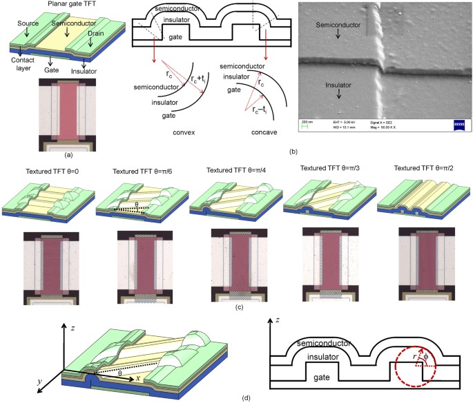
models are corroborated with experiments. Finally, the concept of texture based gain control in TFT voltage amplifiers is demonstrated. RESULTS AND DISCUSSIONS DEVICE GEOMETRIES Figure 1
illustrates the geometries of planar (Fig. 1a) and textured gate (Fig. 1b and c) a-Si:H TFTs that were fabricated using the process flow as described in the Methods section. The texturing
was primarily designed in the form of periodic striations oriented along different directions. The schematic cross-section of metal-insulator-semiconductor stack after texturing is shown in
Fig. 1b. The metal-insulator-stack in the fabricated devices was conformal as shown in the SEM image with the silicon nitride insulator having a thickness _t_ _i_ = 200 nm. The SEM images
of multiple devices are given as Fig. S1 in the Supporting Information. There exist three types of interfaces. Interfaces where the semiconductor presents a convex face to the insulator
(convex regions), interfaces of zero curvature where the metal-insulator-semiconductor stack is planar (planar regions, also as expected in a conventional planar gate TFT) and interfaces
where the semiconductor presents a concave face (concave regions) to the insulator. We define the insulator-semiconductor interface as having a local radius of curvature _r_ _c_ (_x_, _y_).
For the textured a-Si:H TFTs fabricated for experiments in this work, the typical minimum value of _r_ _c_ (_x_, _y_) ~ 250 nm. Defining the _x_-direction and _y_-directions to be along the
channel length and along the channel width, respectively, the striations were made to lie along an angle _θ_ that an in-plane vector makes to the _x_-direction with 0 ≤ _θ _≤ _π_/2 as shown
in Fig. 1c. The striations were also made to extend below the source drain contacts. All TFTs used in this study had a channel width of _W_ = 400 _μ_m. The striations had a height of 200 nm,
planar width of 4 _μ_m and a pitch of ~12 _μ_m. Figure 1d shows the coordinate systems used in this work. For the convex and concave regions we also a define a polar co-ordinate system
(_r_, _ϕ_) with radial coordinate _r_ as it greatly simplifies the analysis. The polar coordinate system maps with the Cartesian system as _x_ = _r_cos(_ϕ_)sin(_θ_), _y_ =
_r_cos(_ϕ_)cos(_θ_) and _z_ = _r_sin(_ϕ_). EXPERIMENTAL RESULTS Figure 2 shows the current-voltage characteristics (I–V characteristics) of TFTs with planar and textured gates with texturing
along _θ_ = 0 and _θ_ = _π_/2. The characteristics are shown for TFTs of different channel lengths, _L_ = 10 _μ_m (Fig. 2a), _L_ = 15 _μ_m (Fig. 2b), _L_ = 40 _μ_m (Fig. 2c) and _L_ = 135
_μ_m (Fig. 2d). Each plot shows the band of standard error obtained by testing four devices for each case and provides a reasonably good estimate of the typical performance of the device.
The color codes of grey, blue and red are used to indicate the characteristics of planar gate TFTs, textured gate TFTs with striations along _θ_ = 0 and textured gate TFTs with striations
along _θ_ = _π_/2, respectively. The labels _I_ _d_ , _V_ _gs_ and _V_ _ds_ indicate the drain-source current, gate-source voltage and the drain-source voltage respectively. Figure 2 shows
the transfer characteristics in linear scale obtained at _V_ _ds_ = 2 V, output characteristics obtained at _V_ _gs_ = 10 V, transfer characteristics in log scale, and the plot of dlog_I_
_d_ /d_V_ _gs_ versus _V_ _gs_ to help identify the sub-threshold slope (peak of the curves), onset of sub-threshold and above threshold conduction (threshold voltage). The mobility for
planar TFTs was observed to be about 0.19 cm2/Vs. Detailed data sets are presented as Figs S2–S5 in the Supporting Information. Figure 3 shows the impact of _θ_ on the performance of
textured TFTs. Using textured TFTs of _L_ = 40 _μ_m channel length having texturing with different _θ_, Fig. 3a shows the transfer characteristics on a linear scale measured at _V_ _ds_ = 2
V, output characteristics measured at _V_ _gs_ = 10 V, transfer characteristics on a log scale and the plot of dlog_I_ _d_ /d_V_ _gs_ versus _V_ _gs_ . Figure 3b and c define the variation
of the effective transconductance d_I_ _d_ /d_V_ _gs_ and sub-threshold swing, respectively. These parameters are extracted from the I–V characteristics and are shown in black markers with
error bars for _θ_ of 0, _π_/6, _π_/4, _π_/3 and _π_/2. The red solid curve in these plots indicate the fit of the elliptical model. The blue dashed curve indicates the value of the
parameter for the planar gate TFT. The methods of extraction of these parameters as well as variations of threshold voltage and leakage current are discussed in the Supporting Information.
It is observed from Fig. 2 that TFTs with texturing along _θ_ = 0 show higher currents as compared with texturing along _θ_ = _π_/2 for all channel lengths. The above threshold current of
textured TFTs with texturing along _θ_ = 0 is higher than planar gate TFTs for small channel lengths but lower than planar gate TFTs for large channel lengths. This trend is reflected in the
plots of the transconductance for various _θ_ as shown in Fig. 3. Furthermore, a trend is observed with the effective transconductance decreasing with increasing _θ_. It is also seen in
both Figs 2 and 3 that the subthreshold swing is typically lower (~0.45 V/dec) in the conventional planar gate TFTs as compared to textured gate TFTs. Variations in _θ_ do not appear to
affect the subthreshold swing significantly and the value remains at ~0.54 V/dec for all _θ_. The threshold voltage too appears unaffected significantly by texturing and is similar (~4.5 V)
for both planar and textured TFTs. It is also unaffected by variations in _θ_ (Figure S6 Supplementary Information). The textured TFTs show a significantly larger drain-source leakage
current as compared to planar gate TFTs. However, the variations in observed leakage currents are too large to discern any trends with variations in _θ_ (Figure S6 Supplementary
Information). SPATIAL MODULATION OF PARAMETERS DUE TO TEXTURING MODULATION OF LOCAL GATE CAPACITANCE PER UNIT AREA, _C_ _I_ (_X_, _Y_) First we consider the impact of texturing on
capacitance of the metal-insulator-semiconductor stack. Since texturing results in the semiconductor-insulator interface having convex, concave and planar regions, i.e. having variations in
the local radius of curvature _r_ _c_ (_x_, _y_), the capacitance per unit area also becomes a function of _x_ and _y_. We define the local value of this capacitance per unit area at any
point (_x_, _y_) and for the elemental section d_x_ by d_y_ by the variable _c_ _i_ (_x_, _y_). The total capacitance of the elemental section is therefore _c_ _i_ d_x_d_y_. In regions where
the metal-insulator-semiconductor stack remains planar (as also in the case of conventional planar gate TFTs), _c_ _i_ (_x_, _y_) = _ε_ _i_ /_t_ _i_ with _ε_ _i_ being the permittivity of
the insulator and _t_ _i_ the thickness. In regions where the semiconductor-insulator interface is convex and having a local radius of curvature, _r_ _c_ , the metal-insulator-semiconductor
stack can be modeled as a cylindrical capacitor _c_ _i_ (_x_, _y_) ~ _ε_ _i_ /(_r_ _c_ ln(1 + (_t_ _i_ /_r_ _c_ ))). In regions where the semiconductor-insulator interface is concave with a
local radius of curvature, _r_ _c_ , _c_ _i_ (_x_, _y_) ~ _ε_ _i_ /(−_r_ _c_ ln(1−(_t_ _i_ /_r_ _c_ ))). In general it can be shown that _c_ _i_ in the convex region is greater than _ε_ _i_
/_t_ _i_ which in turn is greater than the value of _c_ _i_ in the concave region. When _r_ _c_ ≫ _t_ _i_ , _c_ _i_ ~ _ε_ _i_ /_t_ _i_ for all regions. For striated texturing along _θ_,
_r_ _c_ varies along the _π_/2 − _θ_ direction while remaining infinite along the _θ_ direction and _c_ _i_ is also expected to vary along the _π_/2 − _θ_ direction. This spatial modulation
in the local gate capacitance per unit area is responsible for a range of observations. MODULATION OF SURFACE POTENTIAL, _Φ_ _S_ The density of gap states in the semiconductor of the TFT can
be described with an exponential distribution in energy having a characteristic temperature and an equivalent characteristic voltage, _V_ _tc_ . The local potential profile, _φ_, in the
semiconductor would be dependent on the geometry of the metal-insulator-semiconductor stack and is expected to vary with _r_ _c_ . For a given _φ_, the total carrier concentration per unit
volume trapped in the states swept by the Fermi level can be written as \({n}_{t}={n}_{t0}{e}^{\phi /{V}_{tc}}\) with _n_ _t_0 defining the trapped carrier concentration at flat-band. The
free carrier concentration can be defined as \({n}_{f}={n}_{f0}{e}^{\phi /{V}_{th}}\) where _n_ _f_ 0 is the free carrier concentration at flat-band with _V_ _th_ < _V_ _tc_ being the
thermal voltage. The electrostatics of the device is defined by a Poisson-Boltzmann like equation ∇2 _φ_ = _q_(_n_ _t_ + _n_ _f_ )/_ε_ _s_ with _ε_ _s_ being the permittivity of the
semiconductor. In the sub-threshold operation, the Fermi level is located closer to mid gap with _n_ _f_ ≪ _n_ _t_ . However, since _V_ _th_ < _V_ _tc_ , a large enough gate voltage
could result in _n_ _f_ ≫ _n_ _t_ 50. In this analysis, we assume that the electrostatics of the TFT during turn on and just after turn on is mostly dictated by the carriers trapped in the
gap states. On the other hand, the I–V characteristics of the device is defined by _n_ _f_ due to the higher mobility of free carriers. The solution of Poisson’s equation for the case of a
planar metal-insulator-semiconductor stack is well known51. For the convex and concave regions we use a polar co-ordinate system (_r_, _ϕ_) with radial coordinate _r_ as shown in Fig. 1d.
The Poisson Boltzmann equation defining the electrostatics can now be written in polar form as, $${d}^{2}\phi /d{r}^{2}+\mathrm{(1/}r)(d\phi /dr)=q({n}_{t}+{n}_{f})/{\varepsilon }_{s}$$ (1)
It can be shown that (See Supporting Information), _φ_(_r_) ~ 2_V_ _tc_ ln((_κl_ _tc_ /_r_)sec(_κ_ln(_r_/_l_ _b_ ))). Here _l_ _b_ is a characteristic length that scales with _r_ _c_ with
\(\,\mathrm{lim}\,{}_{{r}_{c}\to \infty }({l}_{b}/{r}_{c})=1\) and _l_ _tc_ = (2_ε_ _s_ _V_ _tc_ /_qn_ _t_0)1/2 is a characteristic length equivalent to a Debye length. Also, _κ_ 2 = ((_r_
_c_ ± _t_ _s_ )/_l_ _tc_ )2 − 1 where + is for the concave case, − is for the convex case and _t_ _s_ is the thickness of the semiconductor. The boundary condition is given by Gauss’ law to
be _c_ _i_ (_V_ _gs_ − _V_ _fb_ − _φ_(_r_ = _r_ _c_ )) = ±_ε_ _s_ _ξ_(_r_ = _r_ _c_ ) with _V_ _gs_ is the applied gate-source bias, _V_ _fb_ the flat-band voltage and _ξ_ = −∇_φ_ the
electric field in the semiconductor that is a function of _φ_ and the channel potential. To include the effect of the channel potential, _V_ _ch_ , all potentials can be referenced to the
source electrode. Subsequent to the application of this boundary condition, the surface potential at any point in the channel, _φ_ _s_ , is described by the Lambert-W function, W 0 , as
$${\phi }_{s}={V}_{gs}-{V}_{fb}-{V}_{ch}-2{V}_{tc}{{\bf{W}}}_{{\bf{0}}}(\frac{{\varepsilon }_{s}}{{l}_{tc}{c}_{i}(x,y)}{e}^{({V}_{gs}-{V}_{fb}-{V}_{ch})/2{V}_{tc}})$$ (2) when _V_ _gs_ −
_V_ _fb_ − _V_ _ch_ ≫ 0, we can approximate W 0 (.) ~ ln(.) − ln(ln(.)) and the surface potential is found to scale as, $${\phi }_{s}\sim
2{V}_{tc}\,\mathrm{ln}(\frac{{c}_{i}({V}_{gs}-{V}_{fb}-{V}_{ch})}{q{n}_{t0}{l}_{tc}})$$ (3) In summary, the spatial modulation of the surface potential is due to the spatial modulation of
_c_ _i_ . If however, _V_ _gs_ − _V_ _fb_ − _V_ _ch_ ~ 0, W 0 (0) ~ 0, and _φ_ _s_ ~ _V_ _gs_ − _V_ _fb_ − _V_ _ch_ . Figure 4a shows ATLAS TCAD simulations of the expected variations
in surface potential in the convex, planar and concave regions. MODULATION OF FREE CARRIER CONCENTRATION PER UNIT AREA, _N_ _F_ The discussions so far has looked at the case of the TFT
during turn on with an implicit assumption that _n_ _t_ + _n_ _f_ ~ _n_ _t_ . However for large _V_ _gs_ , the Fermi level would have swept through the gap states and moved significantly
close to the mobility edge and it is possible that _n_ _f_ ≫ _n_ _t_ . Therefore the charge on the gate is compensated for by both, the free carriers and the trapped charge. If the
assumption _n_ _t_ + _n_ _f_ ~ _n_ _f_ is made, one must account for all the trapped charge. This is done by defining a threshold voltage, _V_ _fb_ + _qN_ _t_ /_c_ _i_ , with _N_ _t_
being the trapped carrier concentration per unit area and appropriately modifying _φ_ _s_ . The free carrier concentration per unit area, \({N}_{f}=-{\int }_{{\phi }_{s}}^{0}({n}_{f}/\xi
){\rm{d}}\phi \), can now be defined for both cases, _n_ _t_ ≫ _n_ _f_ and _n_ _f_ ≫ _n_ _t_ , in a generic manner by the use of the variable _V_ _on_ as, $$q{N}_{f}=\gamma
{({c}_{i}({V}_{gs}-{V}_{on}-{V}_{ch}))}^{\alpha }$$ (4) when _n_ _t_ ≫ _n_ _f_ (eg. in sub-threshold operation), _γ_ = (1/_α_)(_n_ _f_0/_n_ _t_0)(_qn_ _t_0 _l_ _tc_ )1−_α_, _α_ = (2_V_ _tc_
/_V_ _th_ ) − 1 and _V_ _on_ = _V_ _fb_ . On the other hand, when _n_ _f_ ≫ _n_ _t_ , _γ_ = 1, _α_ = 1 and _V_ _on_ = _V_ _fb_ + _qN_ _t_ /_c_ _i_ , i.e. a local threshold voltage.
Better estimates of _γ_, _α_ and _V_ _on_ are obtained by smoothing the two regions. Once again it is observed that the spatial modulation of _c_ _i_ not only results in the spatial
modulation of the surface potential but also the free carrier concentration. MODULATION OF THE FIELD EFFECT MOBILITY, _Μ_ In crystalline semiconductor based field effect transistors, the
field effect mobility degrades with an increase in gate voltage due to the increased interaction of carriers with the insulator52. However, the mobility of carriers in disordered
semiconductors is defined by the multiple-trap-release mechanism and it is well established that the mobility, _μ_, increases with increased field effect53. It is only at significantly high
electric fields that any mobility degradation is observed with insulator trapping being a contributor54,55. This increase in field effect can be realized by either increasing the gate
voltage or by increasing _c_ _i_ . Since texturing modulates _c_ _i_ , it is expected that the carriers present in the convex regions experience higher field effect mobility as compared to
the planar regions. The opposite is true for the carriers in the concave regions. The impact of texturing on _μ_ can be quantified by the relation _μ_ = _μ_ 0(_c_ _i_ _t_ _i_ /_ε_ _i_ )_ν_,
with _μ_ 0 being the field effect mobility observed in the planar regions, and _ν_ being a constant coefficient. Once again, the spatial modulation of _c_ _i_ results in the spatial
modulation in _μ_. CUMULATIVE IMPACT OF TEXTURING: I–V CHARACTERISTICS The previous section discussed the spatial modulation of TFT parameters due to texturing. It was established that the
variations in _r_ _c_ in _x_ and _y_ directions resulted in modulating _c_ _i_ , _φ_ _s_ , _N_ _f_ and _μ_ in _x_ and _y_ directions. However, it is the integral or cumulative effect of
these spatial modulations that determine the overall performance of the TFTs. In this section we define the cumulative effect of the local modulations of these parameters and derive the I–V
characteristics. Subsequently, attempts are made to explain the trends observed in Figs 2 and 3. IMPACT ON EFFECTIVE CHANNEL WIDTH AND CHANNEL LENGTH The modulation of the
semiconductor-insulator interface out of plane implies that the effective channel width and effective channel length are now defined by the path length of the path traversed along the
semiconductor-insulator interface in the _y_-direction and _x_-direction, respectively. We define this effective channel width and channel length as _W_ _θ_ and _L_ _θ_ , respectively, with
the subscript _θ_ used to define the orientation angle of the striation and takes the appropriate value for the particular case. If the texturing were removed, both _W_ _θ_ and _L_ _θ_ would
equal the plane projected channel width _W_ and _L_ of a planar gate TFT, respectively. For periodic striated texturing, let _s_ be the projected spatial width of one period in the _π_/2 −
_θ_-direction, and _s_ _θ_ the path length while traversing a path along the semiconductor-insulator interface in the _π_/2 − _θ_ direction. Then, _W_ _θ_ = _s_ _θ_ _W_/_s_ for all _θ_ <
_π_/2. For _θ_ = _π_/2, _W_ _θ_ = _W_ _π_/2 = _W_. Also, _L_ _θ_ = _s_ _θ_ _L_/_s_ for all _θ_ > 0. For _θ_ = 0, _L_ _θ_ = _L_ 0 = _L_. In the particular case of the devices
fabricated in this work, _s_ _θ_ = 12.6 _μ_m and _s_ = 12 _μ_m. Compared to planar gate TFTs, this results in a 5% improvement and attenuation of performance for textured TFTs for _θ_ = 0
and _θ_ = _π_/2, respectively. IMPACT ON THE ONSET OF CONDUCTION Texturing results in the convex regions having a higher values for _N_ _f_ and _μ_ as compared to planar regions. The
opposite is true for concave regions. For the case of textured TFTs with texturing along _θ_ = 0, the channel comprises of flutes of concave, convex and planar regions running from source to
drain. Since the convex regions accumulate free carriers at a lower gate voltage, they permit a current between source and drain much earlier as compared to the planar regions. Thus, the
onset of conduction for textured TFTs with _θ_ = 0 occurs at a lower gate voltage compared to conventional planar gate TFTs. In the case of textured TFTs with texturing along _θ_ = _π_/2,
the channel comprises of flutes of concave, convex and planar regions running along the channel width. Traversing from source to drain, the convex regions having carriers with larger _N_ _f_
and _μ_ would be interspersed with concave regions having low _N_ _f_ and _μ_ akin to a series of high and low resistances. There will therefore be no significant current established in the
TFT till the concave regions also achieve a large enough _N_ _f_ . Thus, textured TFTs with lower _θ_ begin conducting at lower gate voltage. Experiments show a small but definitive trend
in this regard as observed in Fig. 4b for _L_ = 40 _μ_m. _V_ _gs_ at the onset of conduction for other channel lengths are given as Fig. S8 in the Supporting Information. IMPACT ON CONTACT
RESISTANCE The contact resistance of the textured and planar gate TFTs was extracted from the intercept of plot of _V_ _ds_ /_I_ _ds_ versus channel length. This measured value of contact
resistance is plotted in Fig. 4c as a function of _θ_ for textured TFTs (solid black) and for the planar gate TFTs (dashed blue) with the analytical model also shown (red). The contact
resistance for textured TFTs with _θ_ = 0 is seen to be lower than for the planar gate TFTs. The opposite is true for textured TFTs with _θ_ = _π_/2. In general, there appears to be a
gradual trend of increasing contact resistance as _θ_ is increased. The exact mechanics for how the contact resistance is modulated by texturing is not very clear at this point. However,
since the texturing extends below the source drain electrodes, the reasons could be similar to the manner by which the onset of conduction is modulated. This variation in contact resistance
with texturing also explains the dependence of the relative strengths of the TFTs with channel length as observed in Fig. 2. CURRENT VOLTAGE (I–V) CHARACTERISTICS We define the drain to
source current for textured TFTs having texturing along _θ_ to be _I_ _dθ_ where the subscript _θ_ takes the appropriate value for any specific case. It can be shown to be (see Supporting
Information), $$\begin{array}{c}{I}_{d\theta }=\frac{{\mu }_{0}\gamma }{(\alpha +\mathrm{1)(}{\varepsilon }_{i}/{t}_{i}{)}^{\nu }}({\int }_{0}^{{W}_{\theta }}{({\int }_{0}^{{L}_{\theta
}}{c}_{i}^{-\alpha -\nu }{\rm{d}}x)}^{-1}{\rm{d}}y)({({V}_{gs}-{V}_{on}-{I}_{d\theta }{R}_{d\theta })}^{\alpha +1}\\ \,\,\,\,\,\,\,\,\,\,-{({V}_{gs}-{V}_{on}-{V}_{ds}+{I}_{d\theta
}{R}_{d\theta })}^{\alpha +1})\end{array}$$ (5) A more usable form of this model can be developed by making specific assumptions. First for strong above threshold operation, we set _α_ = 1.
Second, the variation in mobility with _c_ _i_ is considered to be minimal and _ν_ = 0. Third, the term _V_ _on_ which represents the threshold voltage for large gate voltages is a constant.
Fourth, for gentle texturing, _W_ _θ_ ~ _W_ and _L_ _θ_ ~ _L_. Using these approximations, $${I}_{d\theta }={\mu }_{0}\gamma ({\int }_{0}^{W}{({\int
}_{0}^{L}{c}_{i}^{-1}{\rm{d}}x)}^{-1}{\rm{d}}y)({V}_{gs}-{V}_{on}-{V}_{ds}\mathrm{/2)(}{V}_{ds}-2{I}_{d\theta }{R}_{d\theta })$$ (6) Figure 4d compares the experimentally obtained I–V
characteristics for the textured TFT with texturing along different _θ_ with the analytical model of Eq. (6). The model is seen to fit remarkably well with the data. In addition to the
purely analytical model of Eq. (6), it is also possible to predict _I_ _dθ_ and the TFT parameters for any _θ_ via an intuitive semi-empirical model. Noting the trends in TFT parameters with
_θ_ as seen in Fig. 3, it is possible to imagine these parameters defining an ellipse. Using this geometric intuition, it is possible to construct a semi-empirical model that defines the
value of the drain-source current and all other TFT parameters for any _θ_ using an elliptical function with the knowledge of their values at _θ_ = 0 and _θ_ = _π_/2. In other words, the
value of these parameters at these points would represent the semi-major and semi-minor axis of the ellipse that could then be plotted on the polar plot of Fig. 3. By this definition,
$${I}_{d\theta }=\frac{{I}_{d0}{I}_{d\frac{\pi }{2}}}{{{(({I}_{d0}\sin (\theta ))}^{2}+{({I}_{d\frac{\pi }{2}}\cos (\theta ))}^{2})}^{1/2}}$$ (7) The values of _I_ _d_0 that would represent
the semi-major axis of the ellipse and _I_ _dπ/2_ that would represent the semi-minor axis of the ellipse can be defined from Eq. (6) to be $$\begin{array}{c}{I}_{d0}={\mu }_{0}\gamma
\frac{{\int }_{0}^{W}{c}_{i}{\rm{d}}y}{L}({V}_{gs}-{V}_{on}-{V}_{ds}\mathrm{/2)(}{V}_{ds}-2{I}_{d0}{R}_{d0})\\ {I}_{d\frac{\pi }{2}}={\mu }_{0}\gamma \frac{W}{{\int
}_{0}^{L}{c}_{i}^{-1}{\rm{d}}x}({V}_{gs}-{V}_{on}-{V}_{ds}\mathrm{/2)}({V}_{ds}-2{I}_{d\frac{\pi }{2}}{R}_{d\frac{\pi }{2}})\end{array}$$ (8) IMPACT ON THE EFFECTIVE CAPACITANCE PER UNIT
AREA, _C_ _I−EFF_ The definition of the local capacitance per unit area, _c_ _i_ (_x_, _y_) is valid for the elemental section d_x_ by d_y_. However, the TFT properties are defined by the
cumulative effect of _c_ _i_ for all elemental section considered in the channel. We define the total effective capacitance per unit area as _C_ _i_−_eff_ . An accurate estimate of _C_
_i_−_eff_ is obtained from Eq. (5) and Eq. (6) where $$\begin{array}{rcl}{C}_{i-eff} & = & \frac{L}{W}({\int }_{0}^{{W}_{\theta }}{({\int }_{0}^{{L}_{\theta }}{c}_{i}^{-\alpha -\nu
}{\rm{d}}x)}^{-1}{\rm{d}}y)\\ & & \sim \frac{L}{W}({\int }_{0}^{W}{({\int }_{0}^{L}{c}_{i}^{-1}{\rm{d}}x)}^{-1}{\rm{d}}y)\end{array}$$ (9) In general, defining the convex to have a
smaller radius of curvature as compared to the concave regions would help increase _C_ _i_−_eff_ . If however, the convex and concave regions have the same radius of curvature, or if the
radius of curvature of the concave region is smaller than the convex region, it is very possible that _C_ _i_−_eff_ < _ε_ _i_ /_t_ _i_ , i.e. less than the effective capacitance per unit
area of a planar gate TFT. For example, if the texturing consists of periodic convex and concave regions with the semiconductor-insulator interface having radius of curvature _r_ _c_ in
both regions, the effective capacitance in one spatial period would scale as ~(_ε_ _i_ /_r_ _c_ )((ln(1 + (_t_ _i_ /_r_ _c_ )))−1 + (ln(1/(1 − (_t_ _i_ /_r_ _c_ ))))−1) and can be shown to
be slightly less than _ε_ _i_ /_t_ _i_ . This also happens to be the case in the experiments of Fig. 2. Figure 4e shows the capacitance-voltage (C-V) characteristics obtained from textured
and planar TFTs. The effective capacitance of the textured TFTs is seen to be slightly lower than the case of the planar gate TFTs. This is also corroborated by the results seen in Fig. 2.
In large channel length TFTs, the relative importance of the channel resistance is more than the contact resistance. On the other hand, in short channel length TFTs, the channel resistance
is much smaller and the contact resistance becomes more important. Hence the ratio of the above threshold current of the textured TFTs to the above threshold current of the planar gate TFT
decreases with increasing channel length. IMPACT ON SUB-THRESHOLD SWING The sub-threshold swing for the TFT is proportional to ln(10)_V_ _tc_ (1 + _C_ _t_ /_C_ _i_−_eff_ ) with _C_ _t_ being
an effective capacitance of trap state. The sub-threshold swing is therefore modulated by _C_ _i_−_eff_ . From the C-V characteristics of Fig. 4e it is seen that _C_ _i_−_eff_ is slightly
lower than _ε_ _i_ /_t_ _i_ . Therefore, it is expected that the planar gate TFTs will have a slightly lower sub-threshold swing (and higher sub-threshold slope) as compared to the textured
TFTs as corroborated by Fig. 3. IMPACT ON THE THRESHOLD VOLTAGE The effective threshold voltage of the TFT is best defined as _V_ _fb_ + _qN_ _t_ /_C_ _i_−_eff_ with _N_ _t_ being the trap
carrier concentration per unit area. From the C-V characteristics of Fig. 4e it is seen that _C_ _i_−_eff_ is slightly lower than _ε_ _i_ /_t_ _i_ . Therefore, it is expected that the planar
gate TFTs will have a slightly lower threshold voltage as compared to the textured TFTs (Corroborated by Fig. S6, Supplementary Information). APPLICATION: VOLTAGE AMPLIFIERS WITH TEXTURED
TFTS We now address the example stated in the introduction to this work and consider the design of a common source amplifier of a certain gain _G_ using TFTs based on a non-complementary
process. If only planar gate TFTs are used, the desired gain can be achieved by ensuring the ratio of the aspect ratios of the driver TFT to the load TFT is _G_ 2. We explore the possibility
of boosting the gain not by the pure scaling of the aspect ratios but instead by also using the fact that the effective ratio of transconductance of the textured TFTs with the planar gate
TFTs vary with _θ_. Figure 5 shows the schematic, micro-graphs and experimental results of two categories of amplifiers investigated. First, common source amplifiers based on the planar gate
TFT with aspect ratio of 400/15 for the driver and 400/135 for the load were tested. The theoretically expected dc gain from this amplifier configuration is 3 while although a gain of about
1 was experimentally observed. The mismatch is attributed to the influence of contact resistance in the driver TFT. Next, amplifiers based on the planar gate TFT for the driver with aspect
ratio 400/15 along with a textured gate TFT with aspect ratio 400/135 and with texturing along _θ_ = _π_/2 for the load were tested. A dc gain of 2 was obtained. This boost in gain is
achieved without altering the effective layout area of the circuit. CONCLUSION This work studied the possibility of controlling the TFT transconductance via the texturing of the gate metal
with specific geometric patterns. The texturing was accomplished via a dual gate metal deposition, the upper deposited metal being patterned. Specific to this study were textures based on
periodic striations oriented along an angle _θ_ with the direction of the channel length. Experiments were performed with a-Si:H TFTs to identify the impact of texturing on the TFT I–V
characteristics and TFT parameters. It was experimentally observed that textured TFTs with _θ_ = 0 have a larger above threshold current, higher transconductance, quicker onset of conduction
and smaller contact resistance as compared to textured TFTs with _θ_ = _π_/2. A continuous trend was observed in all these parameters as _θ_ was increased from 0 to _π_/2. Textured TFTs
with _θ_ = 0 also showed larger above threshold current (upto 40%) as compared to planar gate TFTs when the channel lengths were small. This is believed to be due to combined impact of the
contact resistance and channel resistance. Textured TFTs with _θ_ = _π_/2 consistently showed a lower above threshold current (upto −40%) compared to planar gate TFTs. The subthreshold slope
and effective gate capacitance of planar gate TFTs were observed to be consistently and slightly higher than textured TFTs. These observations could be explained via analytical models. The
key results from the analysis can be summarized as follows. First, texturing results in a modulation of the local radius of curvature, _r_ _c_ , defined for any location (_x_, _y_) with _x_
in the direction of the channel length and _y_ in the direction of the channel width. The modulation in _r_ _c_ causes a modulation in _c_ _i_ , the local gate capacitance per unit area
defined for the elemental section d_x_d_y_. This in turn resulted in the modulation of the local surface potential _φ_ _s_ and the local free carrier concentration per unit area, _N_ _f_
with both _φ_ _s_ and _N_ _f_ being larger in convex regions as compared to concave regions. This explains the quicker turn on of textured TFTs with _θ_ = 0 since the convex regions
accumulate carrier earlier than the planar regions thereby providing a current path from source to drain at a lower gate voltage. On the other hand for the case of _θ_ = _π_/2, the concave
regions must also accumulate carriers before a current path exists between the source and drain. Second, lower contact resistance coupled with the above described behavior results in a
higher above threshold current in short channel textured TFTs with _θ_ = 0 as compared to planar gate TFTs. Third, the cumulative effect of the modulations in _c_ _i_ results in the
effective capacitance per unit area for the TFT, _C_ _i_−_eff_ , being slightly lower than _ε_ _i_ /_t_ _i_ . This explains the lower sub-threshold slope of the textured TFTs as compared to
the planar gate TFTs. Texturing therefore appears to provide an additional and strong control on the TFT parameters alongside aspect ratio and gate voltage based control. Transconductance
modulation via texturing instead permits the use of minimum aspect ratio devices while retaining the ability to modulate transconductance by modulating _θ_. Compared to control via aspect
ratio alone, this approach helps improve spatial resolution and performance as demonstrated by the design of the voltage amplifier. From the point of view of fabrication, texturing is
readily adapted to fabrication methods such as ink-jet printing. METHODS A-SI:H THIN FILM TRANSISTOR FABRICATION Corning glass slide (Corning-2947, 75 mm × 50 mm), pre-cleaned using standard
Piranha solution, was used as the substrate for device fabrication. The gate of the transistor was a 200 nm chromium metal layer deposited using e-beam evaporation and patterned using
optical lithography. In order to create the striations, an additional 200 nm aluminum metal layer was deposited and patterned using photo-lithography. This was followed by the deposition of
200 nm silicon nitride as gate dielectric, 120 nm amorphous hydrogenated silicon (a-Si:H) as the active layer and 30 nm n-doped amorphous silicon (a-Si) as contact layer, all of which were
deposited using plasma enhanced chemical vapor deposition. Subsequently, the active layer (a-Si:H) was patterned to isolate the devices and the insulator layer was patterned to open vias.
Before source/drain electrode metal deposition, the substrate was dipped in dilute hydrofluoric acid for 10 s in order to remove any native oxide on the a-Si:H surface. The source-drain
metal with 200 nm of Cr was deposited using e-beam evaporation and was patterned by lithography. Finally the n-doped a-Si layer was patterned and etched away from regions over the channel.
All devices were designed to have a channel width of 400 _μm_. The striations had a height of 200 _nm_, a width of 4 _μm_ and a pitch of 12 _μm_. The devices were annealed at 150 degrees for
1 hour in ambient conditions before testing. MEASUREMENT OF I-V CHARACTERISTICS The TFT testing was carried out using Keithley 4200 Semiconductor Characterization System inside a probe
station. The source, drain and gate pads of the devices were probed using tungsten probe tips, and were connected to three SMUs (Source Measure Units) of the Keithley through triax cables.
For transfer characteristics, the drain voltage was stepped from 0 to 2 V in steps of 0.5 V. For each step, the gate voltage was swept from 0 to 10 V in steps of 0.1 V. The source SMU was
set at a constant bias of 0 V. The compliance current for all SMUs was 1 mA. For output characteristics, the voltages were interchanged; the gate voltage was stepped from 0 to 10 V in steps
of 2.5 V and for each step, the drain voltage was swept from 0 to 10 V in steps of 0.1 V. For amplifier testing, the four SMUs of the Keithley were connected to the _V_ _dd_ , _V_ _ss_ , _V_
_in_ and _V_ _out_ pads of the circuit. While _V_ _dd_ and _V_ _ss_ , terminals were biased at constant voltages of 10 V and 0 V, the _V_ _in_ SMU was swept from 0 to 10 V, in steps of 0.1
V and the _V_ _out_ SMU was used as a voltmeter to measure the output voltage of the amplifier. MEASUREMENT OF CAPACITANCE-VOLTAGE (C-V) CHARACTERISTICS The C-V measurement was carried out
using Keithley 4200 Semiconductor Characterization System. Cable compensations were carried out to minimize any stray capacitances. The source/drain overlap capacitance to the gate was used
for C-V measurement. A dc bias varying from−15V to +15 V along with a 10 kHz, 10 mV sinusoidal signal was applied between the two SMUs to obtain the C-V characteristics. SIMULATION DETAILS
To analyze the variations in potential in the convex, concave and planar regions, ATLAS TCAD simulations on cylindrical metal-insulator-semiconductor capacitors were designed for simulation.
These were akin to metal-insulator-semiconductor capacitors experiencing tensile or compressive bending. Both the concave and convex geometries were made with 2-D polar coordinates and the
planar structure with 2-D rectangular coordinates. The insulator and the semiconductor were set to be SiN and intrinsic a-Si respectively with the thickness of 200 nm and 150 nm. The gate
metal was chosen to be aluminum with a work-function of 4.1 eV. The radius of curvature (_r_ _c_ ) for the bent geometries was chosen as 1 _μ_m. The arc length (in case of the planar
structure, the length) of the semiconductor insulator interface was 3 _μm_. The effective density of states at the conduction band and the valence band edge of a-Si were chosen to be
2.5e20/cc and 2.5e20/cc, respectively. The band-gap and the electron-affinity of the a-Si were used as 1.8 _eV_ and 3.8 _eV_ respectively. The dielectric constant of SiN and a-Si were 7.5
and 11.8 respectively. The localized tail states and the deep states were modeled using the exponential distribution and the gaussian distribution, respectively. The characteristic energy
and the density of states at the conduction band edge of acceptor-like tail states were 28 meV and 1e22/cc.eV, respectively. The total density of states, the characteristic decay energy and
the peak energy location (with respect to the conduction band edge) of acceptor-like deep states were 1.5e15/cc.eV, 0.15 eV and 0.62 eV, respectively. REFERENCES * Lee, S., Jeon, S., Chaji,
R. & Nathan, A. Transparent semiconducting oxide technology for touch free interactive flexible displays. _Proc. IEEE_ 103, 644–664 (2015). Article Google Scholar * Mativenga, M.,
Geng, D., Kim, B. & Jang, J. Fully transparent and rollable electronics. _ACS Appl. Mater. Interfaces_ 7, 1578–1585 (2015). Article CAS PubMed Google Scholar * Gao, S., Wu, X., Ma,
H., Robertson, J. & Nathan, A. Ultrathin multifunctional graphene-PVDF layers for multidimensional touch interactivity for flexible displays. _ACS Appl. Mater. Interfaces_ 9, 18410–18416
(2017). Article CAS PubMed Google Scholar * Ng, T. N., Wong, W. S., Chabinyc, M. L., Sambandan, S. & Street, R. A. Flexible image sensor array with bulk heterojunction organic
photodiode. _Appl. Phys. Lett._ 92, 213303 (2008). Article ADS Google Scholar * Shin, S. W., Lee, K.-H., Park, J.-S. & Kang, S. J. Highly transparent, visible-light photodetector
based on oxide semiconductors and quantum dots. _ACS Appl. Mater. Interfaces_ 7, 19666–19671 (2015). Article CAS PubMed Google Scholar * Jeon, S. _et al_. Nanometer-scale oxide thin film
transistor with potential for high-density image sensor applications. _ACS Appl. Mater. Interfaces_ 3, 1–6 (2011). Article CAS PubMed Google Scholar * Ng, T. N. _et al_. Scalable
printed electronics: an organic decoder addressing ferroelectric non-volatile memory. _Sci. Rep._ 2, 585 (2012). Article PubMed PubMed Central Google Scholar * Hota, M. K., Alshammari,
F. H., Salama, K. N. & Alshareef, H. N. Transparent flash memory using single _Ta_ 2 _O_ 5 layer for both charge trapping and tunneling dielectrics. _ACS Appl. Mater. Interfaces_ 9,
21856–21863 (2017). Article CAS PubMed Google Scholar * Geier, M. L. _et al_. Solution-processed carbon nanotube thin-film complementary static random access memory. _Nat. Nanotechnol._
10, 944–948 (2015). Article ADS CAS PubMed Google Scholar * Ling, H. _et al_. Synergistic effects of self-doped nanostructures as charge trapping elements in organic field effect
transistor memory. _ACS Appl. Mater. Interfaces_ 8, 18969–18977 (2016). Article CAS PubMed Google Scholar * Kim, Y.-H., Lee, E. Y., Lee, H. H. & Seo, T. S. Characteristics of reduced
graphene oxide quantum dots for a flexible memory thin film transistor. _ACS Appl. Mater. Interfaces_ 9, 16375–16380 (2017). Article CAS PubMed Google Scholar * Petti, L. _et al_. Metal
oxide semiconductor thin-film transistors for flexible electronics. _Appl. Phys. Rev._ 3, 021303 (2016). Article ADS Google Scholar * Hu, Y. _et al_. Self-powered system with wireless
data transmission. _Nano Lett._ 11, 2572–2577 (2011). Article ADS CAS PubMed Google Scholar * Lee, S., Lee, K., Liu, C.-H., Kulkarni, G. S. & Zhong, Z. Flexible and transparent
all-graphene circuits for quaternary digital modulations. _Nat. Commun._ 3, 1018 (2012). Article PubMed Google Scholar * Münzenrieder, N. _et al_. Oxide thin-film transistors on fibers
for smart textiles. _Technologies_ 5, 31 (2017). Article Google Scholar * Du, X., Li, Y., Motley, J. R., Stickle, W. F. & Herman, G. S. Glucose sensing using functionalized amorphous
In–Ga–Zn–O field-effect transistors. _ACS Appl. Mater. Interfaces_ 8, 7631–7637 (2016). Article CAS PubMed Google Scholar * Guo, H. _et al_. All-in-one shape-adaptive self-charging power
package for wearable electronics. _ACS Nano_ 10, 10580–10588 (2016). Article CAS PubMed Google Scholar * Lee, I.-K., Lee, K. H., Lee, S. & Cho, W.-J. Microwave annealing effect for
highly reliable biosensor: dual-gate ion-sensitive field-effect transistor using amorphous InGaZnO thin-film transistor. _ACS Appl. Mater. Interfaces_ 6, 22680–22686 (2014). Article CAS
PubMed Google Scholar * Takeda, Y. _et al_. Fabrication of ultra-thin printed organic TFT CMOS logic circuits optimized for low-voltage wearable sensor applications. _Sci. Rep._ 6, 25714
(2016). Article ADS CAS PubMed PubMed Central Google Scholar * Nakata, S., Arie, T., Akita, S. & Takei, K. Wearable, flexible, and multifunctional healthcare device with an ISFET
chemical sensor for simultaneous sweat pH and skin temperature monitoring. _ACS Sens._ 2, 443–448 (2017). Article CAS PubMed Google Scholar * Subramanian, V. _et al_. Progress toward
development of all-printed RFID tags: materials, processes, and devices. _Proc. IEEE_ 93, 1330–1338 (2005). Article CAS Google Scholar * Myny, K. & Steudel, S. Flexible thin-film NFC
transponder chip exhibiting data rates compatible to ISO NFC standards using self-aligned metal-oxide TFTs. In _2016 IEEE International Solid-State Circuits Conference (ISSCC)_ 298–299
(2016). * Fiore, V. _et al_. An integrated 13.56-MHz RFID tag in a printed organic complementary TFT technology on flexible substrate. _IEEE Trans. Circuits Syst. I: Regular Papers_ 62,
1668–1677 (2015). Article MathSciNet Google Scholar * Kodali, P., Saravanavel, G. & Sambandan, S. Crumpling for energy: Modeling generated power from the crumpling of polymer
piezoelectric foils for wearable electronics. _Flexible and Printed Electronics_ 2, 035005 (2017). Article Google Scholar * Dagdeviren, C. _et al_. Transient, biocompatible electronics and
energy harvesters based on ZnO. _Small_ 9, 3398–3404 (2013). Article CAS PubMed Google Scholar * Kodali, P., Krishna, A., Varun, R., Prasad, M. & Sambandan, S. Segmented electrodes
for piezoelectric energy harvesters. _IEEE Electron Device Lett._ 35, 485–487 (2014). Article ADS Google Scholar * Rieutort-Louis, W. _et al_. Device optimization for integration of
thin-film power electronics with thin-film energy-harvesting devices to create power-delivery systems on plastic sheets. In _IEEE International Electron Devices Meeting (IEDM)_,
12.3.1–12.3.4 (2012). * Prasad, O., Jha, P., Pillai, S., Prasad, M., Bharadwaj, A. & Sambandan, S. Interconnects on Elastomers: Optimizing for Stretchability, Speed and Layout Area. _IOP
Flexible and Printed Electronics_ 2, 045007 (2017). Article Google Scholar * Saravanavel, G., Raghunandan, K. & Sambandan, S. Soft and Morphable Displays and Profilometers:
Self-Assembled Out-of-Plane by Capillary Pressure Acting on a Gel. _IEEE Trans. Electron Devices_ 63, 2023–2028 (2016). Article ADS CAS Google Scholar * Udatha., S. _et al_. Soft and
Morphable Displays and Profilometers: Self-Assembled Out-of-Plane by Capillary Pressure Acting on a Gel. _IEEE Trans. Electron Devices_ 63, 1696–1703 (2016). Article ADS CAS Google
Scholar * Shannon, J. M. & Balon, F. High-performance thin-film transistors in disordered and poor-quality semiconductors. _IEEE Trans. Electron Devices_ 54, 354–358 (2007). Article
ADS CAS Google Scholar * Lee, S. & Nathan, A. Subthreshold schottky-barrier thin-film transistors with ultralow power and high intrinsic gain. _Science_ 354, 302–304 (2016). Article
ADS CAS PubMed Google Scholar * Han, S. & Lee, S. Y. High performance of full swing logic inverter using all n-types amorphous ZnSnO and SiZnSnO thin film transistors. _Appl. Phys.
Lett._ 106, 212104 (2015). Article ADS Google Scholar * Sambandan, S. High-gain amplifiers with amorphous-silicon thin-film transistors. _IEEE Electron Device Lett._ 29, 882–884 (2008).
Article ADS CAS Google Scholar * Shabanpour, R. _et al_. Design and analysis of high-gain amplifiers in flexible self-aligned a-IGZO thin-film transistor technology. _Analog Integrated
Circuits and Signal Processing_ 87, 213–222 (2016). Article Google Scholar * Garripoli, C. _et al_. Analogue frontend amplifiers for bio-potential measurements manufactured with a-IGZO
TFTs on flexible substrate. _IEEE Journal on Emerging and Selected Topics in Circuits and Systems_ 7, 60–70 (2017). Article Google Scholar * Tarn, Y.-C., Ku, P.-C., Hsieh, H.-H. & Lu,
L.-H. An amorphous-silicon operational amplifier and its application to a 4-bit digital-to-analog converter. _IEEE J. Solid-State Circuits_ 45, 1028–1035 (2010). Article Google Scholar *
Shoute, G., Afshar, A., Muneshwar, T., Cadien, K. & Barlage, D. Sustained hole inversion layer in a wide-bandgap metal-oxide semiconductor with enhanced tunnel current. _Nat. Commun._ 7,
10632 (2016). Article ADS CAS PubMed PubMed Central Google Scholar * Cantatore, E. _et al_. A 13.56-MHz RFID system based on organic transponders. _IEEE J. Solid-State Circuits_ 42,
84–92 (2007). Article Google Scholar * Huang, T.-C. & Cheng, K.-T. Design for low power and reliable flexible electronics: Self-tunable cell-library design. _J. Disp. Technol._ 5,
206–215 (2009). Article ADS Google Scholar * Münzenrieder, N., Zysset, C., Kinkeldei, T., Cherenack, K. & Tröster, G. A flexible InGaZnO based 1-bit SRAM under mechanical strain. In
_2011 Semiconductor Conference Dresden (SCD)_ 1–4 (2011). * Seo, J.-H. _et al_. Fast flexible transistors with a nanotrench structure. _Sci. Rep._ 6, 24771 (2016). Article ADS CAS PubMed
PubMed Central Google Scholar * Rotzoll, R. _et al_. Radio frequency rectifiers based on organic thin-film transistors. _Appl. Phys. Lett._ 88, 123502 (2006). Article ADS Google
Scholar * Cai, W., Ma, X., Zhang, J. & Song, A. Transparent thin-film transistors based on sputtered electric double layer. _Materials_ 10, 429 (2017). Article ADS PubMed Central
Google Scholar * Sambandan, S. Influence of gate corrugations on the performance of thin-film transistors. _IEEE Electron Device Lett._ 33, 56–58 (2012). Article ADS Google Scholar *
Aljada, M. _et al_. Structured-gate organic field-effect transistors. _J. Phys. D: Appl. Phys._ 45, 225105 (2012). Article ADS Google Scholar * Amalraj, R. & Sambandan, S. Influence
of curvature on the device physics of thin film transistors on flexible substrates. _J. Appl. Phys._ 116, 164507 (2014). Article ADS Google Scholar * Martins, R. _et al_. Complementary
metal oxide semiconductor technology with and on paper. _Adv. Mater._ 23, 4491–4496 (2011). Article CAS PubMed Google Scholar * Sekine, T., Fukuda, K., Kumaki, D. & Tokito, S. The
effect of mechanical strain on contact resistance in flexible printed organic thin-film transistors. _Flexible and Printed Electronics_ 1, 035005 (2016). Article Google Scholar * Shur, M.
& Hack, M. Physics of amorphous silicon based alloy field-effect transistors. _J. Appl. Phys._ 55, 3831–3842 (1984). Article ADS CAS Google Scholar * Leroux, T. Static and dynamic
analysis of amorphous-silicon field-effect transistors. _Solid-State Electron._ 29, 47–58 (1986). Article ADS CAS Google Scholar * Chen, K. _et al_. Mosfet carrier mobility model based
on gate oxide thickness, threshold and gate voltages. _Solid-State Electron._ 39, 1515–1518 (1996). Article ADS CAS Google Scholar * Hyun, C., Shur, M., Hack, M., Yaniv, Z. &
Cannella, V. Above threshold characteristics of amorphous silicon alloy thin-film transistors. _Appl. Phys. Lett._ 45, 1202–1203 (1984). Article ADS CAS Google Scholar * Lee, S. _et al_.
Trap-limited and percolation conduction mechanisms in amorphous oxide semiconductor thin film transistors. _Appl. Phys. Lett._ 98, 203508 (2011). Article ADS Google Scholar * Dehuff, N.
_et al_. Transparent thin-film transistors with zinc indium oxide channel layer. _J. Appl. Phys._ 97, 064505 (2005). Article ADS Google Scholar Download references ACKNOWLEDGEMENTS Sanjiv
Sambandan thanks the University of Cambridge and the Indian Institute of Science for permitting a joint appointment via the DBT Cambridge Lectureship program. AUTHOR INFORMATION AUTHORS AND
AFFILIATIONS * Department of Instrumentation and Applied Physics, Indian Institute of Science, Bangalore, 560012, India Aswathi Nair, Prasenjit Bhattacharya & Sanjiv Sambandan *
Department of Engineering, University of Cambridge, Cambridge, CB3 0FF, United Kingdom Sanjiv Sambandan Authors * Aswathi Nair View author publications You can also search for this author
inPubMed Google Scholar * Prasenjit Bhattacharya View author publications You can also search for this author inPubMed Google Scholar * Sanjiv Sambandan View author publications You can also
search for this author inPubMed Google Scholar CONTRIBUTIONS A.N. fabricated the devices and performed all experiments, P.B. ran all simulations and verified the models, S.S. conceived the
idea and advised on the experiments and developed the models. All authors reviewed the manuscript. CORRESPONDING AUTHOR Correspondence to Sanjiv Sambandan. ETHICS DECLARATIONS COMPETING
INTERESTS The authors declare that they have no competing interests. ADDITIONAL INFORMATION PUBLISHER'S NOTE: Springer Nature remains neutral with regard to jurisdictional claims in
published maps and institutional affiliations. ELECTRONIC SUPPLEMENTARY MATERIAL SUPPLEMENTARY INFORMATION RIGHTS AND PERMISSIONS OPEN ACCESS This article is licensed under a Creative
Commons Attribution 4.0 International License, which permits use, sharing, adaptation, distribution and reproduction in any medium or format, as long as you give appropriate credit to the
original author(s) and the source, provide a link to the Creative Commons license, and indicate if changes were made. The images or other third party material in this article are included in
the article’s Creative Commons license, unless indicated otherwise in a credit line to the material. If material is not included in the article’s Creative Commons license and your intended
use is not permitted by statutory regulation or exceeds the permitted use, you will need to obtain permission directly from the copyright holder. To view a copy of this license, visit
http://creativecommons.org/licenses/by/4.0/. Reprints and permissions ABOUT THIS ARTICLE CITE THIS ARTICLE Nair, A., Bhattacharya, P. & Sambandan, S. Modulating Thin Film Transistor
Characteristics by Texturing the Gate Metal. _Sci Rep_ 7, 17932 (2017). https://doi.org/10.1038/s41598-017-18111-5 Download citation * Received: 05 October 2017 * Accepted: 05 December 2017
* Published: 20 December 2017 * DOI: https://doi.org/10.1038/s41598-017-18111-5 SHARE THIS ARTICLE Anyone you share the following link with will be able to read this content: Get shareable
link Sorry, a shareable link is not currently available for this article. Copy to clipboard Provided by the Springer Nature SharedIt content-sharing initiative