- Select a language for the TTS:
- UK English Female
- UK English Male
- US English Female
- US English Male
- Australian Female
- Australian Male
- Language selected: (auto detect) - EN
Play all audios:
ABSTRACT Material surfaces encompass structural and chemical discontinuities that often lead to the loss of the property of interest in so-called dead layers. It is particularly problematic
in nanoscale oxide electronics, where the integration of strongly correlated materials into devices is obstructed by the thickness threshold required for the emergence of their
functionality. Here we report the stabilization of ultrathin out-of-plane ferroelectricity in oxide heterostructures through the design of an artificial flux-closure architecture. Inserting
an in-plane-polarized ferroelectric epitaxial buffer provides the continuity of polarization at the interface; despite its insulating nature, we observe the emergence of polarization in our
out-of-plane-polarized model of ferroelectric BaTiO3 from the very first unit cell. In BiFeO3, the flux-closure approach stabilizes a 251° domain wall. Its unusual chirality is probably
associated with the ferroelectric analogue to the Dzyaloshinskii–Moriya interaction. We, thus, see that in an adaptively engineered geometry, the depolarizing-field-screening properties of
an insulator can even surpass those of a metal and be a source of functionality. This could be a useful insight on the road towards the next generation of oxide electronics. SIMILAR CONTENT
BEING VIEWED BY OTHERS IN-SITU MONITORING OF INTERFACE PROXIMITY EFFECTS IN ULTRATHIN FERROELECTRICS Article Open access 16 November 2020 FERROELECTRICITY MODULATES POLARONIC COUPLING AT
MULTIFERROIC INTERFACES Article Open access 15 August 2022 CUMULATIVE POLARIZATION IN CONDUCTIVE INTERFACIAL FERROELECTRICS Article 09 November 2022 MAIN Uncompensated bound charges at the
surfaces of ferroelectric films trigger a depolarizing field1. It is oriented opposite to the spontaneous polarization and highest when this polarization is normal to the surface—the
preferred orientation for ferroelectric devices. Thus, the ferroelectric properties are attenuated with decreasing thickness and completely disappear below about 5 unit cells (u.c.) in most
perovskites2,3. This holds true even when ferroelectrics are deposited on metallic electrodes, all of which have a finite screening length and normally cannot fully compensate for the bound
charges4. To maintain polarization in the ultrathin regime, attempts have been made to minimize the surface-charge accumulation or to enforce polar displacements originating from the
ferroelectric–electrode interface via interface engineering. For instance, interface chemistry can be tailored to create a favourable charge-screening environment and hence net polarization
in the ultrathin regime5. Polar metals were also suggested to eliminate the critical thickness in ferroelectrics by inducing inversion symmetry breaking from the bottom interface6, but their
implementation remains elusive due to the scarcity of lattice-matching systems. The interfacial polarization discontinuity can be avoided with the use of in-plane-polarized ferroelectrics,
which are less susceptible to the depolarizing field even at low thickness7,8. In-plane polarization is, however, incompatible with the coveted state-of-the-art, energy-efficient
out-of-plane capacitor device geometry. Thus, the mutually exclusive benefits of out-of-plane and in-plane-polarized ferroelectrics pose a serious obstacle to the ongoing quest for the next
generation of oxide electronics9,10. Here we combine the ‘best of both worlds’ by eliminating the interfacial polar discontinuity in an out-of-plane-polarized ferroelectric heterostructure
by creating a flux-closure-like11,12 domain architecture. We accomplish this by interfacing two of the most debated out-of-plane-polarized systems, namely, BaTiO3 (BTO) and BiFeO3 (BFO),
with an in-plane-polarized layered ferroelectric of the Aurivillius phase13, that is, Bi5FeTi3O15 (BFTO). In typical perovskite heterostructures, the substrate lattice sets the polarization
anisotropy of the epitaxial heterostructure. In our case, the integration of in-plane-polarized BFTO with out-of-plane-polarized systems provides polarization continuity at the interface and
enables the onset of an out-of-plane ferroelectric polarization from the very first unit cell. The functional impact of the flux-closure-like ferroelectric interface is highlighted in two
ways. First, we demonstrate local switching of the BTO polarization, despite the absence of a conducting bottom electrode. Second, we stabilize homochiral polar Néel domain walls in
multiferroic BFO thin films. We, thus, introduce ferroelectric heterostructures with perpendicular in-plane and out-of-plane polar anisotropies for the design of electric polarization at the
nanoscale, offering a superior alternative to metal-based device paradigms for ferroelectrics. ENFORCING OUT-OF-PLANE POLARIZATION FROM THE FIRST UNIT CELL We begin our investigation by
monitoring the emergence of polarization in a BTO film epitaxially grown on an in-plane-polarized BFTO buffer layer, using optical second-harmonic generation (SHG). This process is sensitive
to inversion symmetry breaking and therefore an ideal probe for ferroelectricity. When measured during the pulsed-laser-deposition process, with in situ second-harmonic generation (ISHG)3
(Methods) one directly accesses the emergence of polarization in ultrathin films with unit-cell accuracy owing to simultaneous monitoring by reflection high-energy electron diffraction. We
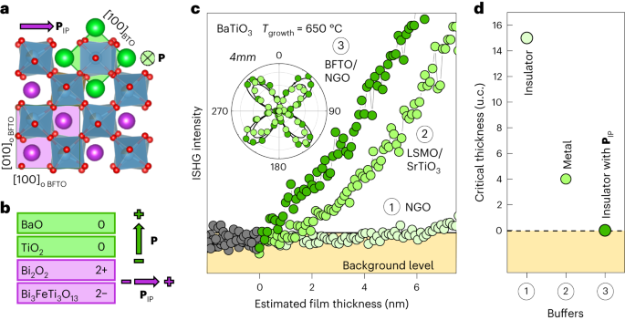
select the Aurivillius compound BFTO as our model in-plane-polarized ferroelectric buffer because it can be grown with single-crystal quality on NdGaO3 (NGO) (001)o (refs. 8,14) (‘o’ denotes
an orthorhombic lattice) and exhibits a robust in-plane polarization from the first half of the unit cell8. Furthermore, BFTO is structurally compatible with functional perovskite oxides
(Fig. 1a), and its charged layered architecture (layer polarization15) can be used to stabilize and orient the out-of-plane polarization3 in ferroelectrics grown on top of it (Supplementary
Note 1). For instance, BFTO favours an upward-pointing polarization in a BTO layer grown on top (Fig. 1b). The absence of an ISHG signal and hence spontaneous polarization during the early
stage of the direct growth of (001)-oriented BTO on the insulating NGO substrate (Fig. 1c) confirms the dominant role of the depolarizing field in a non-charge-screening environment. Only
after passing the thickness of 15 u.c., we detect a signal indicating an out-of-plane-oriented spontaneous polarization. The conventional approach to combat the depolarizing field and reduce
the critical thickness involves the use of a lattice-matching conducting buffer such as La0.7Sr0.3MnO3 (LSMO). Indeed, the associated conduction leads to a substantial improvement in charge
screening. ISHG measurements (Fig. 1c) reveal a reduction in the thickness threshold to 4 u.c. for the onset of ferroelectricity; however, it does not completely eradicate it. We,
therefore, replace the metal with 0.5 u.c. of ferroelectric in-plane-polarized BFTO. Note that the first half of the BFTO unit cell (~2 nm in height) already contains four perovskite layers,
which give rise to the net in-plane polarization and exhibit the full functionality of the Aurivillius compound8,16. At first glance, this substitution seems counterproductive because of
the insulating nature of this polar buffer. However, Fig. 1c shows that we obtain an ISHG signal with the very first BTO unit cell deposited on top of the BFTO; the film grows right in the
ferroelectric phase, without any critical thickness. The subsequent continuous ISHG increase with the ongoing BTO deposition is consistent with an out-of-plane-polarized ferroelectric
single-domain configuration3, characteristic of BTO. SHG polarimetry (Fig. 1c, inset) can be attributed to the tetragonal 4_mm_ point-group symmetry of BTO and hence confirms the
ferroelectric origin of the ISHG signal. Ex situ X-ray diffraction studies confirm the presence of (001)-oriented BTO with the expected epitaxial relationship, involving a 45° in-plane
rotation of the BTO unit cell with respect to the orthorhombic unit cell of the BFTO buffer (Supplementary Note 2). We, thus, see that an in-plane-polarized insulating buffer layer can
surpass metallic electrodes in stabilizing an out-of-plane-polarized ferroelectric state in the ultrathin regime (Fig. 1d). METAL-FREE POLING IN FLUX-CLOSING HETEROSTRUCTURES To shed light
on this seemingly counterintuitive observation, we investigate the ferroelectric domain configuration in our BTO–BFTO bilayer by piezoresponse force microscopy (PFM). The uniform vertical
PFM (VPFM) contrast (Fig. 2a) is consistent with an out-of-plane-polarized single-domain configuration in the top BTO layer of 10 nm thickness as inferred from both ISHG and X-ray
diffraction. The lateral PFM (LPFM) phase scan (Fig. 2b; Supplementary Fig. 3 shows the LPFM amplitude), however, reveals a pattern of 200-nm-wide stripe domains with alternating
tail-to-tail (TT) and head-to-head (HH) charged domain walls (CDWs) characteristic of the buried, fully in-plane-polarized BFTO film of 0.5 u.c. (refs. 8,16). Note that in the Aurivillius
system, such CDWs are known to be nucleated by substrate step edges17. Thus, despite their rigid epitaxial relationship, the BTO and BFTO in the bilayer adhere to their respective polar
anisotropies. The domain configuration of the BTO–BFTO heterostructure, thus, resembles a partial flux closure (Fig. 2c). In contrast to spontaneously forming flux-closure domains (quadrant
domains) within a single material, we achieve this closure by combining two materials with intrinsically different polar axes. In ferroic materials, flux-closure domain formation efficiently
reduces the field energy by forming closed loops of field lines within the material18. Specifically, in ferroelectrics, flux closure11,12 effectively minimizes polarization discontinuities
and bound-charge accumulation at the domain boundaries or interfaces. In our case, this means that the depolarizing field acting on BTO is successfully defeated, allowing the out-of-plane
polarization to establish from the very first unit cell. Remarkably, we observe that the polarization in BTO (5–10 nm) can be reversibly poled with a scanning probe tip (±5 V) (Fig. 2d,e).
Volume-sensitive SHG imaging (Fig. 2f) confirms the ferroelectric nature of the switch and excludes surface-related phenomena as a possible origin of the PFM contrast (Fig. 2d). This is
rather unexpected since ferroelectric poling ordinarily requires the insertion of a conducting bottom electrode. To understand why electric poling in the absence of a metallic bottom contact
is possible, we investigate the BTO poling behaviour with BFTO films of different thicknesses. We find that a minimum thickness of 1.5 u.c. (~6 nm) is required for a BTO polarization switch
(Supplementary Fig. 4). Tomographic PFM19 on a 5-u.c. BFTO film reveals that at this depth, the density of CDWs increases. Tomographic reconstructions with views from both above (Fig. 2g)
and below (Fig. 2h) show that the in-plane-polarized stripe-domain architecture at the bottom interface gradually turns into a random distribution of smaller domains towards the top
interface. We conclude that the increased population of CDWs, and the corresponding density of mobile charges in the buffer layers, emulates the functionality of a counterelectrode (Fig.
2i). Note that the threshold of 1.5 u.c. may be further reduced by selecting alternative Aurivillius compounds with fewer perovskite subunits. The CDW density may also be increased through
the controlled formation of substrate step terraces using higher miscut angles or thermal annealing17. Supplementary Note 3 provides additional technical details related to the
electrode-free poling of the top BTO layer. USING IN-PLANE-POLARIZED BUFFER FOR DOMAIN ENGINEERING So far, we considered an inherently out-of-plane-polarized ferroelectric BTO. Replacing BTO
with a ferroelectric that has its own in-plane polarization components could bring additional degrees of freedom to the ferroelectric domain and domain-wall engineering in our flux-closing
system. To explore this, we grow (001)pc-oriented BFO—the only known robust room-temperature multiferroic—onto the BFTO buffer. Its eight possible polarization directions along the
pseudocubic 〈111〉pc axis20 lead to a rich variety of possible ferroelectric domain and domain-wall configurations with out-of-plane as well as in-plane polarization components. We monitor
the ISHG signal during BFO deposition onto a BFTO layer of a single unit cell. As in the case of BTO, the ISHG yield (Fig. 3a) shows an onset of ferroelectricity in the BFO film with the
first unit cell, thus demonstrating the material-independent potential of our flux-closure-like architecture in defeating depolarizing fields. Post-deposition STEM imaging (Fig. 3b) reveals
the high crystalline quality of our BFO (12 u.c.)–BFTO (1 u.c.)–NGO heterostructure with no dead layer at the BFO–BFTO interface, as highlighted by the averaged dipolar displacements
extracted from this image. The atomically resolved electric-dipole mapping of this interface is displayed in Fig. 3c. To uncover how the interfacial flux closure affects the domain pattern
and the domain-wall architecture in a BFO film of 25 nm, we opt for high-resolution scanning probe measurements for which a fully strained conducting LSMO layer is inserted underneath the
flux-closing BFO–BFTO heterostructure. The charge screening provided by LSMO prevents the formation of domains in the Aurivillius buffer (Supplementary Note 4), which simplifies the PFM
investigations as any LPFM contrast can now be attributed to domain formation in the BFO layer. Note that the insertion of LSMO maintains the respective polar anisotropies in the BFO–BFTO
bilayer and hence its flux-closing properties, as deduced from PFM measurements (Supplementary Notes 4 and 5). The two LPFM brightness levels (Fig. 4a) suggest two in-plane polarization
components in the BFO film. As shown in Supplementary Note 5, these are parallel to the uniaxial polarization axis of the BFTO. The VPFM phase signal is largely uniform (Fig. 4b), aside from
some linear and dot-like discontinuities, which will be discussed later. This is consistent with a downward polarization across the BFO film. Note that this out-of-plane polarization
orientation is opposite to the one stabilized in the BTO films on BFTO and is dictated by both charge accumulation at the interface3,21 and by the similarity between the chemical
compositions of BFO and BFTO. This leads to initial homoepitaxial-like growth and electric dipoles pointing towards the fluorite-like BFTO planes22, as is generally known for Aurivillius
compounds (Supplementary Note 1). Out of the eight possible domain states, the pristine BFO in our heterostructure exhibits only two states, namely, those with a polarization pointing along
[\(11\bar{1}\)]pc or [\(\bar{1}\bar{1}\bar{1}\)]pc, denoted as P1 and P2, respectively (Fig. 4c). This geometry results in the formation of in-plane 109° domain walls, in which—unlike in
commonly observed 109° domain walls in BFO films—the out-of-plane polarization component remains downward oriented from one domain to the other (Fig. 4c). Such a polarization configuration
has never been observed in BFO films and shows that the in-plane-polarized buffer is a powerful tool for domain engineering. STABILIZATION OF POLAR HOMOCHIRAL DOMAIN WALLS IN BFO LPFM and
VPFM images (Fig. 4a–b,d–g) reveal the in-plane and out-of-plane distributions of the BFO polarization associated with its domains and domain walls in both pristine state and after local
electric-field poling using the scanning probe tip, respectively. To our surprise, the domain walls in the VPFM images appear as an alternating sequence of dark (downward polarized) and
bright (upward polarized) lines. This implies a uniform sense of rotation of polarization across all of the walls or, in other words, the BFO domain walls are homochiral (Fig. 5a). The
observed behaviour is drastically different from that of the classical out-of-plane 109° domain walls23, and was confirmed on six different samples. To exclude artifacts in the piezoresponse
data as a trivial explanation for the observed domain-wall homochirality, we verified it with local conduction measurements using conductive atomic force microscopy and detailed PFM
investigations (Supplementary Note 7). Most importantly, high-angle annular dark-field (HAADF) scanning transmission electron microscopy (STEM) imaging confirms the inferred polarization
textures for the BFO domain walls in BFO–BFTO–LSMO (Fig. 5b) for a segment of one of the TT domain walls. Here the atomic displacements mapped for the areas marked with the coloured boxes
highlight a rotation of polarization with an upward-oriented out-of-plane component at this TT wall, in line with the conclusions reached from PFM investigations. The most striking aspect of
this observation is that in the P1–P2 domain wall (Fig. 5a, left), the dipolar reorientation prefers a 251° ‘detour’ over the expected 109° rotation. To highlight the unusual nature of this
state, we propose the notion of a 251° wall in this case. Note that the association of the HH walls to the 109° rotation and the TT walls to the 251° rotation leads to a non-zero net
chirality of ferroelectric domain walls in our heterostructure, which is not exhibited by a BFO film deposited directly onto LSMO (Supplementary Note 8). The homochirality of the BFO domain
walls and the fact that a 251° wall is usually energetically more costly than a 109° wall show that the BFTO buffer exerts a pronounced symmetry-breaking effect. Its manifestation is
reminiscent of the domain-wall homochirality observed in magnetically ordered heterostructures, where it is a consequence of the Dzyaloshinskii–Moriya interaction (DMI)24,25, arising from
symmetry breaking at magnetic surfaces or interfaces. Here, in close analogy, an interface with an in-plane-polarized BFTO layer reduces symmetry and thus appears to give rise to the
non-collinear polar textures that we observe at the BFO domain walls. Mirroring the free-energy invariant describing the DMI in chiral magnets and antiferromagnets26,27,28, the corresponding
DMI-like29 invariant for polarization can be expressed as _E_DM ∝ (_P__x_∂_x__P__z_ − _P__z_∂_x__P__x_), where _x_ corresponds to the in-plane polarization axis and _z_ points to the
out-of-plane one. As for chiral magnets, it sets a deterministic sense of rotation of the order parameter across the domain walls, as we demonstrate in phase-field simulations (Supplementary
Note 9). Such ferroelectric DMI-like interactions have so far mostly been discussed from a theoretical standpoint29,30, and the emergence of 251° domain walls in our BFO films is probably
one of its first experimental observations. All this suggests the use of an in-plane-polarized buffer as an unforeseen route for the stabilization of polar homochirality31,32. OUTLOOK Our
work introduces epitaxial flux-closing heterostructures that stabilize an out-of-plane polarization in ultrathin BTO and BFO right from the very first unit cell. The interfacial symmetry
breaking, occurring between in-plane- and out-of-plane-polarized layers, gives rise to homochirality at the domain walls of the BFO film. In particular, it leads to 251° domain walls in our
BFO films, a probable signature of a DMI-like behaviour in ferroelectrics. These results demonstrate that polar insulators can be more effective than metals in screening the detrimental
depolarizing field in the ultrathin regime. Furthermore, the option to replace the metallic bottom electrodes with an in-plane-polarized buffer may facilitate the downsizing of device
architectures. Both aspects could make the epitaxial combination of perpendicular polar anisotropies a powerful tool in oxide-electronics research. METHODS HETEROSTRUCTURE GROWTH The thin
films and heterostructures were grown on NGO (001)o substrates by pulsed laser deposition, using a KrF excimer laser at 248 nm. The laser fluence, repetition rate, substrate temperature and
growth pressure set for individual layers are as follows: BFTO: 0.9 J cm−2, 2 Hz, 650 °C, 0.075 mbar O2; BTO: 0.9 J cm−2, 2 Hz, 650 °C, 0.015 mbar O2; BFO: 0.7 J cm−2, 8 Hz, 630 °C, 0.125
mbar O2; LSMO: 0.9 J cm−2, 1 Hz, 650 °C, 0.035 mbar O2. The thickness of the thin films was monitored using a combination of reflection high-energy electron diffraction during growth and
X-ray reflectivity ex situ. OPTICAL SHG ISHG was probed in reflection in the pulsed laser deposition growth chamber3. The probe beam of 860 nm (BFO) and 1,200 nm (BTO) was incident onto the
sample with a pulse energy of 20 μJ and onto a spot size of 250 μm in diameter. The ISHG signal was detected using a monochromator and a photomultiplier system3. ISHG plots display an
averaged intensity for every two (Fig. 1c) or three (Fig. 3a) data points measured. An ex situ reflection setup with a 45° angle of incidence was used to obtain a non-zero SHG signal from
the BTO out-of-plane polarization and to spatially resolve the SHG images of poled BTO–BFTO with a pulse energy of 25 μJ. The generated SHG light was collected with a ×20
long-working-distance microscope objective and projected onto a liquid-nitrogen-cooled back-illuminated chip of a charge-coupled device camera (Symphony II, Horiba Jobin Yvon). To gain
domain contrast, an interference technique is employed. Here we took advantage of the SHG light produced by the surface of the BTO film during SHG imaging performed in reflection. This light
does not couple to the ferroelectric order and hence is not affected by the polarization direction. The superposition of the SHG contributions emitted from oppositely polarized areas and
surface contribution leads to constructive and destructive interference33 and results in a pronounced difference in the SHG yield between the upward- and downward-polarized regions. To
account for the 45° reflection geometry, a trapezoidal perspective correction with the following transformation matrix _T_ was applied to all the images with the GIMP software (v. 2.10.24)
to revert the poled region into a square shape. $$T=\left(\begin{array}{lll}1.2405&-0.0382&-21.6563\\ -0.0764&1.0419&1.8580\\
-0.0004&0.0003&1.0000\end{array}\right)$$ PFM The scanning probe microscopy measurements were recorded using an NT-MDT NTEGRA scanning probe microscope and two external SR830 lock-in
detectors (Stanford Research) for the simultaneous acquisition of in-plane and out-of-plane piezoresponse. Data acquisition was performed using a 2.3 V a.c. modulation at 70 kHz applied to
the Pt-coated tip (HQ:NSC35/Pt). Sharp diamond probes (AD-2.8-SS) were used for the high-resolution PFM images. Deflection and torsion modes were recorded when measuring with the cantilever
perpendicular to the uniaxial polarization axis of BFTO/BFO. The LPFM and VPFM images were simultaneously recorded in Cartesian coordinates (using _X_ and _Y_ outputs of the external lock-in
amplifiers) after minimizing the background piezoresponse and calibrating the polarization directions on periodically poled LiNbO3 (ref. 34). The collected data are then transformed into
polar coordinates (_R_ and _θ_) using the following equations: _X_ = _R_ cos(_θ_ + _ϕ_) + _B__X_ and _Y_ = _R_ sin(_θ_ + _ϕ_) + _B__Y_. The phase offset _ϕ_ and components of the background
piezoresponse _B__X_ and _B__Y_ along _X_ and _Y_, respectively, are manually adjusted. PFM phase images are plotted with a phase variation from −180° to 180°, the only exception being the
VPFM images of homochiral BFO domain walls, as the scale from 0° to 180° helps to visualize the corresponding phase changes at the domain walls in the uniformly downward-polarized BFO film.
PFM TOMOGRAPHY Tomographic atomic force microscopy (AFM) is based on sequential AFM imaging and probe-based nanomechanical sample milling35. Operating in the PFM mode19, specifically when
biasing the conducting tip with an a.c. field oscillating at the torsional contact resonance, volumetrically mapping the in-plane domain contrast is possible. A PFM tomogram constructed from
a sequence of 95 images, all in the same field of view but for gradually diminishing film thicknesses, is presented in Fig. 2g,h, which overall comprises more than one million 15.7 × 15.7 ×
1.0 nm3 voxels of local piezoresponse signals. The colour contrast depicts the product of the measured amplitude and the sign of the phase for in-plane torsion of the cantilever, which is
the lateral piezoresponse. The AFM equipment (Asylum Research Cypher VRS) is operated in the contact mode using doped diamond probes (AppNano DD-ACTA). A setpoint of approximately 2.24 μN is
sufficient to mill this specimen, whereas torsional PFM imaging is performed with a 1 V peak-to-peak a.c. bias at a frequency of approximately 2.8 MHz. The amplitude and phase of the
locally vibrating lever are simultaneously acquired via a lock-in amplifier (Zurich Instruments MFLI). STEM Cross-sectional specimens were prepared by focused-ion-beam milling with an FEI
Helios NanoLab 660 G3 UC instrument. HAADF-STEM imaging was attained with an FEI Titan Themis microscope equipped with a spherical-aberration probe corrector (CEOS DCOR) operated at 300 kV.
A probe semi-convergence angle of 18 mrad was set in combination with an annular semi-detection range of the HAADF detector of 66–200 mrad. The atomic column positions in the HAADF-STEM
images were fitted with picometre precision36,37. In Figs. 3b and 5b, the Δ_z_ and Δ_x_ polar displacements of the B-site atomic columns in the image plane from the centre of their two
nearest A-site neighbours are along the [100]pc and [011]pc directions, respectively. DATA AVAILABILITY The dataset that supports the findings of this study is available via the ETH Zurich
Research Collection at https://doi.org/10.3929/ethz-b-000626823. REFERENCES * Mehta, R. R., Silverman, B. D. & Jacobs, J. T. Depolarization fields in thin ferroelectric films. _J. Appl.
Phys._ 44, 3379–3385 (1973). Article CAS Google Scholar * Fong, D. D. et al. Ferroelectricity in ultrathin perovskite films. _Science_ 304, 1650–1653 (2004). Article CAS Google Scholar
* De Luca, G. et al. Nanoscale design of polarization in ultrathin ferroelectric heterostructures. _Nat. Commun._ 8, 1419 (2017). Article Google Scholar * Junquera, J. & Ghosez, P.
Critical thickness for ferroelectricity in perovskite ultrathin films. _Nature_ 422, 506–509 (2003). Article CAS Google Scholar * Strkalj, N. et al. In-situ monitoring of interface
proximity effects in ultrathin ferroelectrics. _Nat. Commun._ 11, 5815 (2020). Article CAS Google Scholar * Puggioni, D., Giovannetti, G. & Rondinelli, J. M. Polar metals as
electrodes to suppress the critical-thickness limit in ferroelectric nanocapacitors. _J. Appl. Phys._ 124, 174102 (2018). Article Google Scholar * Keeney, L. et al. Ferroelectric behavior
in exfoliated 2D Aurivillius oxide flakes of sub-unit cell thickness. _Adv. Electron. Mater._ 6, 1901264 (2020). Article CAS Google Scholar * Gradauskaite, E. et al. Robust in-plane
ferroelectricity in ultrathin epitaxial Aurivillius films. _Adv. Mater. Interfaces_ 7, 2000202 (2020). Article CAS Google Scholar * Garcia, V. & Bibes, M. Ferroelectric tunnel
junctions for information storage and processing. _Nat. Commun._ 5, 4289 (2014). Article CAS Google Scholar * Müller, M., Efe, I., Sarott, M. F., Gradauskaite, E. & Trassin, M.
Ferroelectric thin films for oxide electronics. _ACS Appl. Electron. Mater._ 3, 1314–1334 (2023). Article Google Scholar * McQuaid, R. G., McGilly, L. J., Sharma, P., Gruverman, A. &
Gregg, J. M. Mesoscale flux-closure domain formation in single-crystal BaTiO3. _Nat. Commun._ 2, 404 (2011). Article CAS Google Scholar * Tang, Y. L. et al. Observation of a periodic
array of flux-closure quadrants in strained ferroelectric PbTiO3 films. _Science_ 348, 547–551 (2015). Article CAS Google Scholar * Aurivillius, B. Mixed bismuth oxides with layer
lattices. 1. The structure type of CaNb2Bi2O9. _Ark. Kemi._ 1, 463–480 (1949). CAS Google Scholar * Gradauskaite, E., Gray, N., Campanini, M., Rossell, M. D. & Trassin, M. Nanoscale
design of high-quality epitaxial Aurivillius thin films. _Chem. Mater._ 33, 9439–9446 (2021). Article CAS Google Scholar * Spaldin, N. A., Efe, I., Rossell, M. D. & Gattinoni, C.
Layer and spontaneous polarizations in perovskite oxides and their interplay in multiferroic bismuth ferrite. _J. Chem. Phys._ 154, 154702 (2021). Article CAS Google Scholar * Keeney, L.
et al. Persistence of ferroelectricity close to unit-cell thickness in structurally disordered Aurivillius phases. _Chem. Mater._ 32, 10511–10523 (2020). Article CAS Google Scholar *
Gradauskaite, E., Hunnestad, K. A., Meier, Q. N., Meier, D. & Trassin, M. Ferroelectric domain engineering using structural defect ordering. _Chem. Mater._ 34, 6468–6475 (2022). Article
CAS Google Scholar * Kittel, C. _Introduction to Solid State Physics_ 8th edn (John Wiley and Sons, 2005). * Steffes, J. J., Ristau, R. A., Ramesh, R. & Huey, B. D. Thickness scaling
of ferroelectricity in BiFeO3 by tomographic atomic force microscopy. _Proc. Natl Acad. Sci. USA_ 116, 2413–2418 (2019). Article CAS Google Scholar * Streiffer, S. K. et al. Domain
patterns in epitaxial rhombohedral ferroelectric films. I. Geometry and experiments. _J. Appl. Phys._ 83, 2742–2753 (1998). Article CAS Google Scholar * Yu, P. et al. Interface control of
bulk ferroelectric polarization. _Proc. Natl Acad. Sci. USA_ 109, 9710–9715 (2012). Article CAS Google Scholar * Campanini, M., Trassin, M., Ederer, C., Erni, R. & Rossell, M. D.
Buried in-plane ferroelectric domains in Fe-doped single-crystalline Aurivillius thin films. _ACS Appl. Electron. Mater._ 1, 1019–1028 (2019). Article CAS Google Scholar * Chu, Y. H. et
al. Nanoscale control of domain architectures in BiFeO3 thin films. _Nano Lett._ 9, 1726–1730 (2009). Article CAS Google Scholar * Emori, S., Bauer, U., Ahn, S. M., Martinez, E. &
Beach, G. S. Current-driven dynamics of chiral ferromagnetic domain walls. _Nat. Mater._ 12, 611–616 (2013). Article CAS Google Scholar * Vélez, S. et al. High-speed domain wall
racetracks in a magnetic insulator. _Nat. Commun._ 10, 4750 (2019). Article Google Scholar * Dzyaloshinskii, I. E. Theory of helicoidal structures in antiferromagnets. I. Nonmetals. _Sov.
Phys. JETP_ 19, 960–971 (1964). Google Scholar * Bogdanov, A. N., Rößler, U. K., Wolf, M. & Müller, K. H. Magnetic structures and reorientation transitions in noncentrosymmetric
uniaxial antiferromagnets. _Phys. Rev. B_ 66, 214410 (2002). Article Google Scholar * Landau, L. D. & Lifshitz, E. M. _Statistical Physics: Volume 5_ 2nd edn (Pergamon Press, 1969). *
Zhao, H. J., Chen, P., Prosandeev, S., Artyukhin, S. & Bellaiche, L. Dzyaloshinskii-Moriya-like interaction in ferroelectrics and antiferroelectrics. _Nat. Mater._ 20, 341–345 (2021).
Article CAS Google Scholar * Erb, K. C. & Hlinka, J. Vector, bidirector, and Bloch skyrmion phases induced by structural crystallographic symmetry breaking. _Phys. Rev. B_ 102, 024110
(2020). Article CAS Google Scholar * Chauleau, J.-Y. et al. Electric and antiferromagnetic chiral textures at multiferroic domain walls. _Nat. Mater._ 19, 386–390 (2020). Article CAS
Google Scholar * Fusil, S. et al. Polar chirality in BiFeO3 emerging from a peculiar domain wall sequence. _Adv. Electron. Mater._ 8, 2101155 (2022). Article CAS Google Scholar *
Trassin, M., Luca, G. D., Manz, S. & Fiebig, M. Probing ferroelectric domain engineering in BiFeO3 thin films by second harmonic generation. _Adv. Mater._ 27, 4871–4876 (2015). Article
CAS Google Scholar * Soergel, E. Piezoresponse force microscopy (PFM). _J. Phys. D: Appl. Phys._ 44, 464003 (2011). Article Google Scholar * Song, J., Zhou, Y., Padture, N. P. &
Huey, B. D. Anomalous 3D nanoscale photoconduction in hybrid perovskite semiconductors revealed by tomographic atomic force microscopy. _Nat. Commun._ 11, 3308 (2020). Article CAS Google
Scholar * Yankovich, A. B. et al. Picometre-precision analysis of scanning transmission electron microscopy images of platinum nanocatalysts. _Nat. Commun._ 5, 4155 (2014). Article CAS
Google Scholar * Campanini, M., Erni, R., Yang, C. H., Ramesh, R. & Rossell, M. D. Periodic giant polarization gradients in doped BiFeO3 thin films. _Nano Lett._ 18, 717–724 (2018).
Article CAS Google Scholar Download references ACKNOWLEDGEMENTS E.G. and M.T. acknowledge the Swiss National Science Foundation under project no. 200021_188414. M.T. and M.F. acknowledge
support by the EU European Research Council under Advanced Grant Program no. 694955-INSEETO. Q.N.M. acknowledges support by the Swiss National Science Foundation under project no.
P2EZP2_191872. M.C., A.V. and M.D.R. acknowledge support by the Swiss National Science Foundation under project no. 200021_175926. M.F. acknowledges support by the Swiss National Science
Foundation under project no. 200021_178825. We thank K. Dörr for fruitful discussions. FUNDING Open access funding provided by Swiss Federal Institute of Technology Zurich AUTHOR INFORMATION
AUTHORS AND AFFILIATIONS * Department of Materials, ETH Zurich, Zurich, Switzerland Elzbieta Gradauskaite, Natascha Gray, Martin F. Sarott, Tizian Scharsach, Manfred Fiebig & Morgan
Trassin * Univ. Grenoble Alpes, CEA, LITEN, DEHT, Grenoble, France Quintin N. Meier * Electron Microscopy Center, Empa, Dübendorf, Switzerland Marco Campanini, Alexander Vogel & Marta D.
Rossell * Department of Materials Science and Engineering, University of Connecticut, Storrs, CT, USA Thomas Moran, Karla Del Cid-Ledezma & Bryan D. Huey Authors * Elzbieta Gradauskaite
View author publications You can also search for this author inPubMed Google Scholar * Quintin N. Meier View author publications You can also search for this author inPubMed Google Scholar
* Natascha Gray View author publications You can also search for this author inPubMed Google Scholar * Martin F. Sarott View author publications You can also search for this author inPubMed
Google Scholar * Tizian Scharsach View author publications You can also search for this author inPubMed Google Scholar * Marco Campanini View author publications You can also search for this
author inPubMed Google Scholar * Thomas Moran View author publications You can also search for this author inPubMed Google Scholar * Alexander Vogel View author publications You can also
search for this author inPubMed Google Scholar * Karla Del Cid-Ledezma View author publications You can also search for this author inPubMed Google Scholar * Bryan D. Huey View author
publications You can also search for this author inPubMed Google Scholar * Marta D. Rossell View author publications You can also search for this author inPubMed Google Scholar * Manfred
Fiebig View author publications You can also search for this author inPubMed Google Scholar * Morgan Trassin View author publications You can also search for this author inPubMed Google
Scholar CONTRIBUTIONS All authors discussed the results. E.G. and M.T. wrote the manuscript with M.F. The thin-film growth, ISHG measurements and structural analysis were performed by E.G.
Scanning probe microscopy measurements were done by E.G. together with N.G. and T.S. The phase-field simulations were performed by Q.N.M., in addition to the development of electrostatic
models. M.F.S. performed the SHG imaging ex situ. M.C., A.V. and M.D.R. carried out the STEM investigations. T.M., K.D.C.-L. and B.D.H. performed the tomographic PFM study. M.T. designed the
experiment with E.G. and jointly supervised the work with M.F. CORRESPONDING AUTHORS Correspondence to Elzbieta Gradauskaite or Morgan Trassin. ETHICS DECLARATIONS COMPETING INTERESTS The
authors declare no competing interests. PEER REVIEW PEER REVIEW INFORMATION _Nature Materials_ thanks Josh Agar, Neus Domingo and Vincent Garcia for their contribution to the peer review of
this work. ADDITIONAL INFORMATION PUBLISHER’S NOTE Springer Nature remains neutral with regard to jurisdictional claims in published maps and institutional affiliations. SUPPLEMENTARY
INFORMATION SUPPLEMENTARY INFORMATION Supplementary Notes 1–9, Figs. 1–21 and Tables 1 and 2. RIGHTS AND PERMISSIONS OPEN ACCESS This article is licensed under a Creative Commons Attribution
4.0 International License, which permits use, sharing, adaptation, distribution and reproduction in any medium or format, as long as you give appropriate credit to the original author(s)
and the source, provide a link to the Creative Commons license, and indicate if changes were made. The images or other third party material in this article are included in the article’s
Creative Commons license, unless indicated otherwise in a credit line to the material. If material is not included in the article’s Creative Commons license and your intended use is not
permitted by statutory regulation or exceeds the permitted use, you will need to obtain permission directly from the copyright holder. To view a copy of this license, visit
http://creativecommons.org/licenses/by/4.0/. Reprints and permissions ABOUT THIS ARTICLE CITE THIS ARTICLE Gradauskaite, E., Meier, Q.N., Gray, N. _et al._ Defeating depolarizing fields with
artificial flux closure in ultrathin ferroelectrics. _Nat. Mater._ 22, 1492–1498 (2023). https://doi.org/10.1038/s41563-023-01674-2 Download citation * Received: 14 March 2022 * Accepted:
25 August 2023 * Published: 02 October 2023 * Issue Date: December 2023 * DOI: https://doi.org/10.1038/s41563-023-01674-2 SHARE THIS ARTICLE Anyone you share the following link with will be
able to read this content: Get shareable link Sorry, a shareable link is not currently available for this article. Copy to clipboard Provided by the Springer Nature SharedIt content-sharing
initiative