- Select a language for the TTS:
- UK English Female
- UK English Male
- US English Female
- US English Male
- Australian Female
- Australian Male
- Language selected: (auto detect) - EN
Play all audios:
ABSTRACT The photoexcitation of heterostructures consisting of metallic nanoclusters and a semiconductor has been extensively investigated in relation to interests in photocatalysis and
optical devices. The optoelectronic functions of the heterostructures originate from localized surface plasmon resonance, which can induce electron and resonance energy transfers. While it
is well known that photoinduced electronic interaction between a metallic nanocluster and a semiconductor is responsible for the resonance energy transfer, the electron transfer associated
with the photoinduced electronic interaction has not been discussed. In this paper, we elucidate the photoexcitation dynamics of a silver nanocluster/TiO2 heterostructure using an original
first-principles computational approach that explicitly deals with light–matter interactions. It is shown that the photoinduced silver–TiO2 electronic interaction causes excited electrons to
be directly transferred from the silver nanocluster to the TiO2 layer without passing through the conduction band of the silver nanocluster. SIMILAR CONTENT BEING VIEWED BY OTHERS
LONG-LIVED MODULATION OF PLASMONIC ABSORPTION BY BALLISTIC THERMAL INJECTION Article 09 November 2020 CHARGED BIEXCITON POLARITONS SUSTAINING STRONG NONLINEARITY IN 2D SEMICONDUCTOR-BASED
NANOCAVITIES Article Open access 31 August 2023 HOT CARRIERS FROM INTRA- AND INTERBAND TRANSITIONS IN GOLD-SILVER ALLOY NANOPARTICLES Article Open access 01 August 2024 INTRODUCTION The
photoexcitation of heterostructures consisting of metallic nanoclusters and a semiconductor has been extensively investigated in relation to interests in optically functional materials, such
as photonic devices, solar cells, and photocatalysis.1,2,3,4 The localized surface plasmon resonance (LSPR) of metallic nanoclusters plays a central role in the optoelectronic functions of
these heterostructures. The collective electron oscillation of LSPR generates an intense electric field that is much larger than that of an incident laser. Because of the generated electric
field, the photoinduced electronic interaction between metallic nanoclusters and a semiconductor remarkably enhances the photoexcitation intensity of the semiconductor while diminishing the
collective electron oscillation; that is, LSPR causes resonance energy transfer from the metallic nanoclusters to the semiconductor.1,3 Meanwhile, photoabsorption by LSPR largely generates
excited electrons that transfer from a metallic nanocluster to its surrounding materials.2,4 This excited-electron transfer by LSPR has been discussed separately from the photoinduced
electronic interaction; however, the two can be simultaneously induced. In practice, experimental studies of heterostructures consisting of silver nanoclusters and TiO2 have reported both
electron transfer and resonance energy transfer caused by the photoinduced electronic interaction.5,6 In addition, the strong electronic coupling at the metal–semiconductor interface and the
mixing of their electronic states is thought to induce direct metal-to-semiconductor electron transfer, and suppress the loss of excited electrons.7 In this context, it is increasingly
necessary to investigate the role of the photoinduced electronic interaction at the metal–semiconductor interface in electron transfer by LSPR. Extensive theoretical and computational
studies have attempted to elucidate optical phenomena such as LSPR. Metallic nanoclusters are often approximated as a macroscopic classical model characterized by a complex dielectric
function for describing the electric field of LSPR.8,9,10 Although first-principles calculations of photoinduced electron transfer in nanomaterials have gradually become more popular,11,12
the number of such studies is still severely limited comparing to those on small molecules and bulk materials due to the large computational cost. In particular, to calculate LSPR of a noble
metal nanocluster is difficult because a large number of electrons (i.e., s- and d-electrons) should be explicitly treated.13 So far, the electron transfer by LSPR associated with
light–matter interactions has not been investigated with the electronic relaxation after the termination of a laser pulse being the main focus of previous first-principles studies. Indeed,
to deal with light–matter interactions is essential for describing the electric field of LSPR, which is the collective electron oscillation synchronized with the incident laser field.
Because the electron transfer and electronic interaction induced by LSPR have been studied individually, the relationship between the two is not understood. In this study, we elucidate the
mechanism of photoexcited electron transfer in a silver nanocluster/TiO2 heterostructure using a first-principles computational program developed by our group.14 In this program, the
electron dynamics caused by light–matter interactions is directly simulated in real time; thus, various optical processes including the photocurrent generation of nanomaterials can be
described.13,15,16 Furthermore, because of the high parallel efficiency, this program can be applied to nanomaterials such as a heterostructure consisting of a silver nanocluster and a TiO2
layer. It is shown that the electron transfer is governed by the photoinduced electronic interaction between a silver nanocluster and a TiO2 layer, and has a substantially different
mechanism from that of the conventional electron transfer by LSPR. Insights into this mechanism can be applied in the design of various optically functional materials with high light-energy
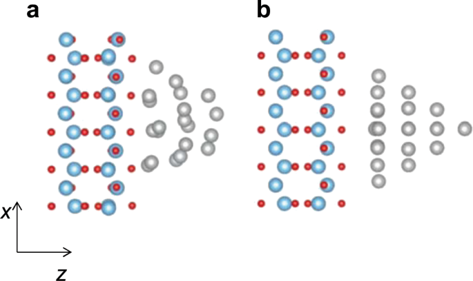
conversion efficiency. RESULTS SIMULATED SYSTEMS Figure 1a shows the optimized structure of a silver/TiO2 heterostructure, which consists of an Ag20 nanocluster and a TiO2 layer. We employ
the slab model of TiO2(110) that has been utilized in previous studies.17,18 The Ag–O bond distances are 2.1–2.5 Å, which is close to previous computational results for heterostructures
consisting of a silver nanocluster and a TiO2 layer.19,20 In the following, the fully optimized Ag20/TiO2 heterostructure is denoted as system A. We also calculated two ideal Ag20/TiO2
systems (B and C), in which the Ag20 nanocluster and the TiO2 layer were separately optimized. The isolated Ag20 nanocluster has the tetrahedral geometrical structure that has previously
been used to investigate optical responses involving the LSPR of a silver nanocluster.21,22 We consider this tetrahedral structure to be better than a spherical one for modeling an adsorbed
metallic nanocluster that tends to form a planar structure. The Ag–O bond distances for ideal system B (Fig. 1b) are 3.0–3.3 Å, which is about 1 Å longer than that for system A. As the Ag20
nanocluster becomes closer to the TiO2 layer, electronic transitions that are not found in system A become noticeable (Supplementary Sec. 1). Ideal system C is almost the same as system B
(and is thus omitted from Fig. 1), except that the Ag–O bond distances are 4.0–4.2 Å, slightly larger than the sum of the van der Waals radii of ~3.7 Å.23 System C is used to investigate the
electron transfer associated with the photoinduced electronic interaction between the silver nanocluster and the TiO2 layer. Although we calculate a larger Ag84/TiO2 heterostructure system,
no remarkable dependence on the nanocluster size is observed in the electron transfer mechanism described below. Thus, we mainly discuss the Ag20/TiO2 heterostructures in the following
text. For the systems considered in this paper, we calculate the photoexcited electron dynamics using our original computational program SALMON (Scalable Ab-initio Light–Matter simulator for
Optics and Nanoscience), in which the time-dependent Kohn–Sham equation is calculated explicitly dealing with light–matter interactions in real time and real space.14 The laser intensity
and the pulse duration are set to 109 W cm−2 and 30 fs, respectively. FUNDAMENTAL ELECTRONIC AND OPTICAL PROPERTIES Figure 2a shows a map of the two-dimensional (2D) local density of states
(LDOS) of system A. The horizontal axis is the _z_-direction perpendicular to the TiO2 layer. The TiO2 and silver moieties are in the left and right, respectively. The Ag20–TiO2 interface is
at _z_ ≃ 13–14 Å. The vertical axis is the band energy _E_ relative to the Fermi level. Valence band states in the silver moiety from −1 to 0 eV are occupied by ~10 electrons, and analogous
states are recognized from the isolated silver nanocluster. Localized states in the TiO2 moiety around −0.3 eV are absent from the isolated TiO2 layer, and are regarded as gap states
created by Ag–O chemical bonds. Although evanescent metal states caused by a surface termination can generate delocalized gap sates,24 such gap states play a minor role in photoexcitation
discussed below. The further details of the electronic structure are given in Supplementary Sec. 2. In the conduction band, the LDOS in the silver moiety is lower than that in the TiO2
moiety. Therefore, photoexcited electrons tend to transfer into the conduction band of TiO2, that is, into a high-DOS region. Although this tendency is observed in our first-principles
simulation of the photoexcited electron dynamics shown below, the feature of the electron transfer cannot be rationalized solely by the character of the DOS. Figure 2b shows the optical
absorption spectra with _x_-polarization for the tetrahedral Ag20 nanocluster, TiO2 layer, system A, and ideal system B. The edge of the optical absorption energy of the TiO2 layer is ~2.7
eV, ~0.3 eV lower than that of bulk rutile TiO2.25 This underestimation is a result of employing the conventional Perdew–Burke–Ernzerhof (PBE) functional. Note that the purpose of this study
is to elucidate the mechanism of electron transfer in the silver nanocluster/TiO2 heterostructure related with the photoinduced electronic interaction between the silver nanocluster and the
TiO2 layer. Because the absorption spectrum of the Ag20 nanocluster has a peak at ~3 eV, our approach can reproduce the experimental condition whereby a silver nanocluster and a TiO2 layer
are simultaneously excited by a laser pulse with an energy of ~3 eV.6 Thus, we consider that the dependence on the functional of the density functional theory (DFT) does not affect the
discussion at the qualitative level. In the following, we mainly discuss the photoexcited electron dynamics by a 3.0-eV laser. It is noted that we change the laser frequency from 3.0 eV to
2.8 eV at which system A has the absorption peak, and confirmed that the mechanism of the photoexcited electron transfer in system A is qualitatively unchanged. PHOTOEXCITED ELECTRON
DYNAMICS Figure 3 shows 2D maps of the variation in the electron occupation number at _t_ = 30 fs induced by an _x_-polarized laser pulse with an energy of 3.0 eV. The definition of the
horizontal and vertical axes is the same as that of Fig. 2a. The red and blue distributions indicate that the electron occupation numbers are greater and less than that in the ground state,
respectively. Thus, electrons are excited from blue areas to red areas. White arrows depict an energy gap of 3.0 eV, which is equal to the incident laser energy. In the isolated TiO2 layer
(Fig. 3a), 3.0-eV electronic transitions take place. As seen from Fig. 3b, a number of distributions are found in the conduction band of the Ag20 nanocluster truncated from system A. These
distributions are also attributed to 3.0-eV electronic transitions (the white arrows). Figure 3c illustrates the 2D map for system A. A remarkable change caused by the silver–TiO2 contact
can be observed in the silver moiety; no electron occupation is found in the conduction band at all (white rounded box), even though the occupation numbers decrease in the valence band. A
recent experimental study on a heterostructure with silver nanoclusters and TiO2 also reported that excited electrons are almost absent from the conduction band of the silver moiety.6 In
Fig. 3c, small electronic excitation from the gap states ~−0.3 eV is found, and an analogous result has been also reported in the experimental study. Figure 3d shows possible electronic
transition paths for a silver nanocluster/TiO2 heterostructure. The change in electronic transitions caused by the silver–TiO2 contact exhibited in Fig. 3 indicates that direct electron
transfer from the silver moiety to the TiO2 layer (path III) is induced while excited-electron generation in the silver moiety (path II) substantially diminishes. Indeed, as the
time-dependent photoexcitation process proceeds, no excited electrons are found in the conduction band of the silver moiety (Supplementary Fig. 4). For comparison, we further investigate the
dependence of the photoexcitation on the distance between the Ag20 nanocluster and the TiO2 layer using the ideal systems. The variation in the occupation number at _t_ = 30 fs is shown in
Fig. 4. The direct electron transfer is also induced in system B (Fig. 4a), in which the Ag20 nanocluster rather weakly contacts with the TiO2 layer compared with system A. Furthermore, a
larger heterostructure consisting of Ag84 and TiO2 yields the direct electron transfer (Supplementary Fig. 8). Therefore, the direct electron transfer is not a singular phenomenon caused by
atomistic details of Ag–O chemical bonds or by a small silver nanocluster. For system C (Fig. 4b), in which Ag–O distances are slightly longer than the van der Waals contact distance,
excited electrons clearly accumulate in the silver nanocluster, and the conventional LSPR-induced electron transfer from the silver nanocluster to the TiO2 layer (i.e., path IV in Fig. 3d)
takes place. Figures 3 and 4 show that the direct electron transfer is significantly different from the conventional electron transfer that has been discussed in previous studies. The
difference between systems A, B, and C can be made clearer by numerically evaluating the variation in the occupation number. The occupation number in the valence band of the silver moiety
decreases by 1.2 × 10⁻², 3.4 × 10⁻², and 3.3 × 10⁻² for systems A, B, and C, respectively. In the conduction band, the occupation number in the silver moiety increases by 8.6 × 10⁻⁴, 4.6 ×
10−3, and 1.4 × 10⁻² for systems A, B, and C, respectively. It is clearly shown that photoexcited electrons almost completely transfer from the silver moiety into the TiO2 moiety for systems
A and B, whereas remains in the silver moiety as excited electrons for system C. The difference in the direct electron transfer from the conventional LSPR-induced case is reflected in the
photoexcited electron dynamics. Figure 5 shows the _z_ component of the time-dependent electronic polarization, _P__z_(_t_) defined by Eq. (6), where the _z_ is the direction perpendicular
to the TiO2 layer. As time elapses, a negative electronic polarization is induced by the laser field, and is attributed to the electron transfer from the silver moiety to the TiO2 layer.
Although the magnitude of the polarization for system A is smaller than that for the ideal systems, this is simply because the photoexcitation intensity of the silver moiety in system A is
smaller than that of the tetrahedral Ag20 nanocluster. Independent of the difference in the geometrical structure, the electron transfer is almost terminated just after the incident laser is
switched off (_t_ = 30 fs) in systems A and B. In contrast, for system C, the polarization continues to increase, even after the laser is switched off. The time-dependence reflects the
mechanism of the electron transfer: the direct electron transfer occurs simultaneously with the electronic transition, whereas the conventional LSPR-induced electron transfer takes place
after the electronic transition in the silver nanocluster. An analogous time-dependence to Fig. 5 can be obtained by analyzing the electron density and the variation in the occupation number
(Supplementary Figs 4–7, 9). Note that our simulation do not take into account the energy relaxation of excited electrons originating from electron–electron and electron–phonon scatterings.
The electron–electron scattering due to the large electron oscillation of LSPR causes the fast decay of the electronic excitation in ~10 fs.2,4 Because our approach cannot describe
inelastic electron–electron scattering, the conventional LSPR-induced electron transfer is probably overestimated compared with the direct electron transfer. A many-body description such as
the GW approximation is required to describe the inelastic electron–electron scattering.26 The relaxation by the electron–phonon coupling occurs on time scales from 100 fs to 1 ps,2,4 which
are clearly longer than the experimental decay rate for a silver nanocluster/TiO2 system, ~10 fs.6 Thus, the electron–phonon coupling would play a minor role in the direct electron transfer
although is important after the direct electron transfer is completed (e.g., in carrier recombination and carrier transport in TiO2). PHOTOINDUCED ELECTRONIC INTERACTION To reveal the
driving force of the direct electron transfer, it is important to analyze the photoinduced electronic interaction under light irradiation. This is because LSPR is primarily ascribed to the
photoinduced electronic interaction rather than interband transitions.27,28 Furthermore, LSPR induces various optical phenomena that are not realized only by small molecules and bulk
materials.29,30 Indeed, the direct electron transfer of the present systems is not readily rationalized from transition dipole moments; even though not directly induced by the _x_-polarized
field, the electronic transition along the _z_-direction is preferentially induced over the conventional electronic transition inside the silver moiety. To reveal the mechanism of the
electron transfer, Fig. 6a shows the real part of the _z_ component of the Fourier-transformed photoinduced electric field. This field is coherent in phase with the incident laser field,
namely, it is governed by light–matter interactions. The red and blue colors indicate that the respective electric fields are turned to the opposite direction to each other. The electric
field is substantially distributed in the Ag–O contact region (green dotted circles). This is attributed to the mutual electronic polarization of the silver nanocluster and the TiO2 layer,
as schematically illustrated in Fig. 6b. Because of the difference in DOS between the silver and TiO2 moieties (Fig. 2a), the electric field along the _z_-direction mainly induces electronic
transitions from the silver moiety to the TiO2 moiety (green arrows in Fig. 6b). As the silver–TiO2 distance increases, the mutual electronic polarization becomes weaker; thus, the direct
electron transfer does not occur for system C, in which the photogenerated electric field is smaller than that in system B (Supplementary Fig. 10). In other words, the direct electron
transfer is governed by the light–matter interaction that causes the photoinduced electronic interaction in the silver–TiO2 interfacial region. DISCUSSION In numerous studies on the
photoexcitation of heterostructures consisting of metallic nanoclusters and a semiconductor, it has been assumed that electrons pass through the conduction band of the metallic
nanoclusters.2,4 The excited electrons accumulated in metallic nanoclusters lose their energy through electron–phonon and electron–electron scatterings, seriously reducing the efficiency of
electron transfer into a semiconductor. Thus, direct electron transfer is capable of yielding high-efficiency light-energy conversion. If a metal is in close contact with a semiconductor,
electronic transitions occur between interfacial states, resulting in direct electron transfer.31,32 However, because interfacial states are delocalized in both the metal and semiconductor
moieties, excited electrons are partially generated in the metal moiety. In contrast, the present electron transfer is induced in ideal system B with a weak silver–TiO2 contact, and excited
electrons are not found in the silver moiety. Furthermore, electronic states participating in the electron transfer are recognized from the isolated silver nanocluster and the TiO2 layer.
Therefore, the direct electron transfer revealed in this study is significantly different from that between interfacial states. Although interfacial gap states do not participate in the
electron transfer for the present employed systems, it is expected that the interface modification alters the efficiency of the direct electron transfer. For instance, gap-state-assisted
electron transfer31,32 would be induced by modifying the interfacial region. It is also noted that to select a metallic species suitable for photocurrent generation requires detailed
considerations. For example, to replace silver with gold is favorable for preventing carrier recombination by the band bending in a semiconductor near the Schottky barrier because of the
higher vacuum level of gold than that of silver. However, the photogenerated electric field from gold is smaller than that from silver; that is, to replace silver with gold is inappropriate
for inducing the direct electron transfer. Because of these complex factors, for improving the efficiency of photocurrent generation, it is needed to carefully design the details of the
system (e.g., the size and shape of nanoclusters, and an employed semiconductor). In conclusion, we have elucidated photoexcited electron transfer in heterostructures consisting of a silver
nanocluster and a TiO2 layer using our original first-principles computational approach, which explicitly deals with light–matter interactions. Excited electrons transfer from the silver
nanocluster to the TiO2 layer without passing through the conduction band of silver. The photoinduced electronic interaction at the silver–TiO2 interface is responsible for direct electron
transfer with a mechanism that is significantly different from the conventional LSPR-induced electron transfer. While the proposed mechanism is new, we believe that the direct electron
transfer would have occurred in previous experimental studies without being recognized. This is because no singular interfacial electronic state is needed—it is only necessary to make the
distance between a silver nanocluster and a TiO2 layer shorter than the van der Waals contact distance. According to this rather lax requirement, analogous direct electron transfer would be
induced in metal/semiconductor heterostructures other than silver/TiO2 systems. By actively developing metal/semiconductor heterostructures on the basis of the insights reported in this
paper, the efficiency of light-energy conversion should be improved. In this regard, this study provides a general concept that can be applied in the design of optically functional materials
consisting of metal/semiconductor heterostructures. For further improving the functionality of these materials, it would be required to obtain deeper atomic-scale insights into the
interfacial region. To obtain the insights, our first-principles approach is highly useful because of the wide applicability, for example, to the variation in optical functions depending on
defects and contaminants at the interface. METHODS THEORETICAL FORMULA In SALMON, the photoexcited electron dynamics is simulated by solving the time-dependent Kohn–Sham equation.14
$$i\frac{\partial }{\partial t}{\psi }_{jk}\left({\bf{r}},t\right)=\left[-\frac{1}{2}{\nabla }^{2}-i{\bf{A}}(t)\cdot \nabla
+\frac{1}{2}{{\bf{A}}}^{2}(t)+{v}_{{\rm{nuc}}}({\bf{r}})+{v}_{{\rm{H}}}({\bf{r}},t)+{v}_{{\rm{XC}}}({\bf{r}},t)\right]{\psi }_{jk}\left({\bf{r}},t\right),$$ (1) where _v_nuc is the nuclear
attraction potential, _v_xc is the exchange correlation (XC) potential, _v_H is the Hartree potential, and A is the vector potential of an external field. Equation (1) is directly solved at
three-dimensional Cartesian grid points by a nine-point finite-difference formula in the space derivatives.33,34 The time propagation is evaluated by the fourth-order Taylor expansion
method. Because of the simplicity of this algorithm, the program has high parallel efficiency and can be applied to nanometer-scale heterostructures by carrying out massively parallel
calculations. From the time-dependent wave function, the electric conductivity _σ__α_ (_α_ ∈ _x_, _y_, _z_) and dielectric function _ϵ__α_ are obtained from the following formulas: $${\sigma
}_{\alpha }(\omega)=\frac{\int {\mathrm{d}}t{e}^{i\omega t}{J}_{\alpha }(t)}{\int {\mathrm{d}}t{e}^{i\omega t}{E}_{{\rm{ext}}}(t)},$$ (2) $${\epsilon }_{\alpha }(\omega)=1+\frac{4\pi
i{\sigma }_{\alpha }(\omega)}{\omega }.$$ (3) Here, _E_ext(_t_) is the electric field of the laser pulse polarized along the _α_ direction, and _J__α_(_t_) is electric current following
through the unit cell defined as35,36 $$\begin{array}{lll}{J}_{\alpha }(t)=\displaystyle\frac{1}{\Omega }\mathop{\int }\nolimits_{\Omega }\sum _{jk}{\rm{Re}}\left[{\psi }_{jk}^{*
}\left({\bf{r}},t\right)\left(-i{{\boldsymbol{\nabla }}}_{\alpha }+\displaystyle\frac{1}{c}{{\bf{A}}}_{\alpha }(t)\right){\psi }_{jk}\left({\bf{r}},t\right)\right]\\ &&+\,i{\sum
\limits_{jk}}\displaystyle\int d{\bf{r}}d{\bf{r}}^{\prime} {\psi }_{jk}^{* }\left({\bf{r}},t\right)\left\{{V}_{{\rm{nonloc}}}({\bf{r}},{\bf{r}}^{\prime}){{\bf{r}}}_{\alpha
}^{\prime}-{{\bf{r}}}_{\alpha }{V}_{{\rm{nonloc}}}({\bf{r}},{\bf{r}}^{\prime})\right\}{\psi }_{jk}\left({\bf{r}},t\right),\end{array}$$ (4) where Ω is the system volume, and _V_nonloc is
caused by the nonlocality of the pseudopotential. We define the optical absorption intensity as \({\alpha }_{2}\equiv {z}_{{\rm{s}}}{\rm{Im}}[\epsilon ]/(4\pi)\), where _z_s is the supercell
length perpendicular to the TiO2 layer. When the vacuum region is sufficiently large, _α_2 is almost independent of the unit cell size.37 We calculate the electron dynamics using a laser
pulse with an electric field given by $${{\bf{E}}}_{{\rm{ext}}}(t)={E}_{0}\hat{{\bf{u}}}{\rm{cos}}\left(\omega t\right){\mathrm{sin}}^{2}\left(\pi t/\tau \right),$$ (5) where
\(\hat{{\bf{u}}}\) is a unit vector along the Cartesian axis, _ω_ is the laser frequency, _E_0 is the amplitude of the incident laser field, and _τ_ is the pulse width. The laser intensity
_I_ (W cm−2) is given with _E_0 (V m−1) as \({E}_{0}=27.45\sqrt{I}\). The vector potential A is defined with Eext as \({\bf{A}}(t)=-{\int
}_{0}^{t}{{\bf{E}}}_{{\rm{ext}}}(t^{\prime}){\rm{d}}t^{\prime}\).14 The time-dependent electronic polarization _P_(_t_) induced by the external laser field is then evaluated using the
following formula: $${P}_{\alpha }(t)={\int }_{0}^{t}{J}_{\alpha }(t^{\prime}){\mathrm{d}}t^{\prime} .$$ (6) Equation (6) is available for both the perpendicular and parallel polarizations
to the TiO2 layer. The variation in the electron occupation number is defined by the following equations:15 $${c}_{ljk}(t)={f}_{jk}(t=0){\left|\left\langle {\psi }_{jk}({\bf{r}},t)| {\psi
}_{lk}({\bf{r}},t=0)\right\rangle \right|}^{2},$$ (7) $${{\mathcal{D}}}_{lk}(E\equiv {\varepsilon }_{lk},z,t)=\sum _{j}{c}_{ljk}(t)\int {\left|{\psi
}_{lk}({\bf{r}},t=0)\right|}^{2}{\mathrm{d}}x{\mathrm{d}}y,$$ (8) $$\Delta {{\mathcal{D}}}_{lk}(E,z,t)={{\mathcal{D}}}_{lk}(E,z,t)-{{\mathcal{D}}}_{lk}(E,z,t=0).$$ (9) Here, _ε_ is a band
energy in the ground state, and _f__j__k_ is the electron occupation number defined by the Fermi–Dirac distribution. In Eq. (7), the photoexcited orbital _ψ__j__k_(R, _t_) is projected onto
the ground-state orbital _ψ__l__k_(R, _t_ = 0).38 By integrating over the _x_ and _y_ directions in Eq. (8), the electronic excitation is illustrated along the _z_-direction, which is
perpendicular to the TiO2 layer. Equation (9) gives the variation in \({{\mathcal{D}}}_{lk}\) caused by the laser field. The \(\Delta {{\mathcal{D}}}_{lk}\) are summed with respect to _l_
and _k_ after Lorentzian broadening has been applied to \(\Delta {{\mathcal{D}}}_{lk}\); thereby, we obtain the variation in the electron occupation number. The Kohn–Sham orbitals are,
strictly speaking, just an auxiliary construct for obtaining the total electron density.39,40 However, the photoexcited electron transfer cannot be fully investigated by only analyzing the
electron density. This is because electrons remaining in the valence band also transfer due to an electric field generated by excited electrons. Thus, from the electron density, we can
evaluate only the total electron transfer in which electrons in both the valence and conduction bands participate. It is noted that the Kohn–Sham orbitals have been widely utilized to get
qualitative interpretations.39 Therefore, the analysis based on Eqs. (7)–(9) is valuable, at least, for obtaining insights into the mechanism of the photoexcited electron transfer. The
photoinduced electronic interaction is analyzed using the Fourier-transformed electric field at the incident laser frequency:41 $$\Delta {\mathcal{E}}({\bf{r}},\omega)\equiv \int {\int
}_{0}^{T}\left\{\rho \left({\bf{r}}^{\prime} ,t\right)-\rho \left({\bf{r}}^{\prime} ,0\right)\right\}\cdot \frac{{\bf{r}}-{\bf{r}}^{\prime} }{| {\bf{r}}-{\bf{r}}^{\prime} {| }^{3}}\cdot
\left\{1-3{(t/T)}^{2}+2{(t/T)}^{3}\right\}{e}^{i\omega t}{\mathrm{dtd}}{\bf{r}}^{\prime} ,$$ (10) where the cubed and squared terms reduce the numerical noise due to the Fourier
transformation,42 and _T_ is set to the pulse width, i.e., 30 fs. As a cosine-type laser field is employed (Eq. (5)), the real part (i.e., the cosine component) of \(\Delta {\mathcal{E}}\)
is attributed to electronic polarization by the incident laser field, whereas the imaginary part (i.e., the sine component) reflects the photoabsorption.41 To obtain the 2D LDOS, we
calculate the following quantity: $${{\mathcal{D}}}_{lk}(E\equiv {\varepsilon }_{lk},z)={f}_{lk}(t=0)\int {\left|{\psi }_{lk}({\bf{r}},t=0)\right|}^{2}{\mathrm{dxdy}}.$$ (11) Then,
lorentzian broadening is applied to \({{\mathcal{D}}}_{lk}\), and the sum with respect to _l_ and _k_ is performed. COMPUTATIONAL DETAILS Geometry optimization was performed using the
Quantum Espresso program package.43 A rutile TiO2(110) surface was employed and the cell size was fixed to that of the bulk system. We further calculated a twice thicker TiO2(110) layer,
which was also utilized in the previous study,18 and confirmed that the results are, at least, qualitatively unchanged in terms of the discussions given in this study (Supplementary Sec. 8).
The dispersion-corrected PBE functional was employed to calculate the exchange correlation potential to take into account van der Waals interactions.44,45,46,47 The optimized systems were
used in calculating the optical response with SALMON.14 The grid spacings were set to ~0.25 Å, in accordance with the unit cell size. The supercell length along the direction perpendicular
to the TiO2 layer was set to 30 Å. This makes the width of the vacuum region ~12 Å. The PBE functional was used in the SALMON calculations. Comparing the computational and experimental
results of optical absorption, we concluded that the functional dependence has a qualitatively negligible influence on the discussion of this study (see also the Results section). It is
noted that the dispersion-corrected functional employed in the geometrical optimization semiempirically corrects the total energy by utilizing a geometrical structure, and does not directly
modify optical properties when the geometrical structure is fixed in the photoexcitation process. Effective core potentials were obtained using the Troullier–Martins scheme implemented in
the fhi98PP program.48,49 Visualizations were performed with the VESTA program package.50 In this study, the _x_-polarized excitation is mainly discussed. Due to the finiteness of the
employed system, the absorption intensity by the _z_-polarized field is several times smaller than that by the _x_-polarized field (Supplementary Secs. 7, 8). It is noted that the direct
electron transfer is also induced by the _z_-polarized field, as well as the experimental study.6 Thus, we consider that the discussion of this study is, at least, qualitatively in accord
with the experimental study. DATA AVAILABILITY The data that support the findings of this study are available from the corresponding author upon reasonable request. REFERENCES * Atwater, H.
A. & Polman, A. Plasmonics for improved photovoltaic devices. _Nat. Mater_ 9, 205–213 (2010). CAS Google Scholar * Clavero, C. Plasmon-induced hot-electron generation at
nanoparticle/metal-oxide interfaces for photovoltaic and photocatalytic devices. _Nat. Photon_ 8, 95–103 (2014). CAS Google Scholar * Li, J. et al. Plasmon-induced resonance energy
transfer for solar energy conversion. _Nat. Photon_ 9, 601–607 (2015). CAS Google Scholar * Brongersma, M. L., Halas, N. J. & Nordlander, P. Plasmon-induced hot carrier science and
technology. _Nat. Nanotech._ 10, 25–34 (2015). CAS Google Scholar * Kazuma, E., Sakai, N. & Tatsuma, T. Nanoimaging of localized plasmon-induced charge separation. _Chem. Commun._ 47,
5777–5779 (2011). CAS Google Scholar * Tan, S. et al. Plasmonic coupling at a metal/semiconductor interface. _Nat. Photonics_ 11, 806–812 (2017). CAS Google Scholar * Wu, K., Chen, J.,
McBride, J. R. & Lian, T. Efficient hot-electron transfer by a plasmon-induced interfacial charge-transfer transition. _Science_ 349, 632–635 (2015). CAS Google Scholar * Vukovic, S.,
Corni, S. & Mennucci, B. Fluorescence enhancement of chromophores close to metal nanoparticles. Optimal setup revealed by the polarizable continuum model. _J. Phys. Chem. C_ 113, 121–133
(2008). Google Scholar * Chen, H., McMahon, J. M., Ratner, M. A. & Schatz, G. C. Classical electrodynamics coupled to quantum mechanics for calculation of molecular optical properties:
a RT-TDDFT/FDTD approach. _J. Phys. Chem. C_ 114, 14384–14392 (2010). CAS Google Scholar * Liu, P., Chulhai, D. V. & Jensen, L. Single-molecule imaging using atomistic near-field
tip-enhanced raman spectroscopy. _ACS Nano_ 11, 5094–5102 (2017). CAS Google Scholar * Wang, L., Long, R. & Prezhdo, O. V. Time-domain ab initio modeling of photoinduced dynamics at
nanoscale interfaces. _Ann. Rev. Phys. Chem._ 66, 549–579 (2015). CAS Google Scholar * Provorse, M. R. & Isborn, C. M. Electron dynamics with real-time time-dependent density
functional theory. _Inter. J. Quant. Chem._ 116, 739–749 (2016). CAS Google Scholar * Iida, K., Noda, M., Ishimura, K. & Nobusada, K. First-principles computational visualization of
localized surface plasmon resonance in gold nanoclusters. _J. Phys. Chem. A_ 118, 11317–11322 (2014). CAS Google Scholar * Noda, M. et al. Scalable ab-initio light-matter simulator for
optics and nanoscience. _Comput. Phys. Commun._ 235, 356–365 (2019). CAS Google Scholar * Iida, K., Noda, M. & Nobusada, K. Photoinduced electron transfer at the interface between
heterogeneous two-dimensional layered materials. _J. Phys. Chem. C_ 122, 21651–21658 (2018). CAS Google Scholar * Yamada, S., Noda, M., Nobusada, K. & Yabana, K. Time-dependent density
functional theory for interaction of ultrashort light pulse with thin materials. _Phys. Rev. B_ 98, 245147 (2018). CAS Google Scholar * Liu, L., McAllister, B., Ye, H. & Hu, P.
Identifying an O2 supply pathway in CO oxidation on Au/TiO2 (110): a density functional theory study on the intrinsic role of water. _J. Am. Chem. Soc._ 128, 4017–4022 (2006). CAS Google
Scholar * Vilhelmsen, L. B. & Hammer, B. Identification of the catalytic site at the interface perimeter of au clusters on rutile TiO2 (110). _ACS Catal._ 4, 1626–1631 (2014). CAS
Google Scholar * Jia, C., Zhang, G., Zhong, W. & Jiang, J. A first-principle study of synergized O2 activation and CO oxidation by Ag nanoparticles on TiO2 (101) support. _ACS Appl.
Mater. Inter._ 8, 10315–10323 (2016). CAS Google Scholar * Puigdollers, A. R., Schlexer, P. & Pacchioni, G. Gold and silver clusters on TiO2 and ZrO2 (101) surfaces: role of dispersion
forces. _J. Phys. Chem. C_ 119, 15381–15389 (2015). CAS Google Scholar * Zhao, L., Jensen, L. & Schatz, G. C. Pyridine-ag20 cluster: a model system for studying surface-enhanced raman
scattering. _J. Am. Chem. Soc._ 128, 2911–2919 (2006). CAS Google Scholar * Sanchez-Gonzalez, A., Munoz-Losa, A., Vukovic, S., Corni, S. & Mennucci, B. Quantum mechanical approach to
solvent effects on the optical properties of metal nanoparticles and their efficiency as excitation energy transfer acceptors. _J. Phys. Chem. C_ 114, 1553–1561 (2010). CAS Google Scholar
* Batsanov, S. S. Van der waals radii of elements. _Inorg. Mater._ 37, 871–885 (2001). CAS Google Scholar * Wager, J. F. & Kuhn, K. Device physics modeling of surfaces and interfaces
from an induced gap state perspective. _Crit. Rev. Solid State_ 42, 373–415 (2017). CAS Google Scholar * Amtout, A. & Leonelli, R. Optical properties of rutile near its fundamental
band gap. _Phys. Rev. B_ 51, 6842–6851 (1995). CAS Google Scholar * Chulkov, E. et al. Electronic excitations in metals and at metal surfaces. _Chem. Rev._ 106, 4160–4206 (2006). CAS
Google Scholar * Bursi, L., Calzolari, A., Corni, S. & Molinari, E. Quantifying the plasmonic character of optical excitations in nanostructures. _ACS Photon_ 3, 520–525 (2016). CAS
Google Scholar * Zhang, R. et al. How to identify plasmons from the optical response of nanostructures. _ACS Nano_ 11, 7321–7335 (2017). CAS Google Scholar * Jain, P. K., Ghosh, D., Baer,
R., Rabani, E. & Alivisatos, A. P. Near-field manipulation of spectroscopic selection rules on the nanoscale. _Proc. Natl Acad. Sci. USA_ 109, 8016–8019 (2012). * Rivera, N., Kaminer,
I., Zhen, B., Joannopoulos, J. D. & Soljačić, M. Shrinking light to allow forbidden transitions on the atomic scale. _Science_ 353, 263–269 (2016). CAS Google Scholar * Zhang, Y. et
al. Surface-plasmon-driven hot electron photochemistry. _Chem. Rev._ 118, 2927–2954 (2017). Google Scholar * Tan, S. et al. Coherent electron transfer at the Ag/graphite heterojunction
interface. _Phys. Rev. Lett._ 120, 126801 (2018). CAS Google Scholar * Chelikowsky, J. R., Troullier, N. & Saad, Y. Finite-difference-pseudopotential method: electronic structure
calculations without a basis. _Phys. Rev. Lett._ 72, 1240 (1994). CAS Google Scholar * Chelikowsky, J. R., Troullier, N., Wu, K. & Saad, Y. Higher-order finite-difference
pseudopotential method: an application to diatomic molecules. _Phys. Rev. B_ 50, 11355 (1994). CAS Google Scholar * Yabana, K., Shinohara, Y., Otobe, T., Iwata, J.-I. & Bertsch, G. F.
_Advances in Multi-Photon Processes and Spectroscopy_, Vol. 18 (WORLD SCIENTIFIC, 2008). * Yabana, K., Nakatsukasa, T., Iwata, J.-I. & Bertsch, G. Real-time, real-space implementation of
the linear response time-dependent density-functional theory. _Phys. Stat. Sol. (b)_ 243, 1121–1138 (2006). CAS Google Scholar * Yang, L., Deslippe, J., Park, C.-H., Cohen, M. L. &
Louie, S. G. Excitonic effects on the optical response of graphene and bilayer graphene. _Phys. Rev. Lett._ 103, 186802 (2009). Google Scholar * Otobe, T. et al. First-principles electron
dynamics simulation for optical breakdown of dielectrics under an intense laser field. _Phys. Rev. B_ 77, 165104 (2008). Google Scholar * Stowasser, R. & Hoffmann, R. What do the
Kohn-Sham orbitals and eigenvalues mean? _J. Am. Chem. Soc._ 121, 3414–3420 (1999). CAS Google Scholar * Ullrich, C. A. _Time-Dependent Density-Functional Theory: Concepts and
Applications_ (OUP Oxford, 2011). * Iida, K., Noda, M. & Nobusada, K. Interface electronic properties between a gold core and thiolate ligands: effects on an optical absorption spectrum
in Au133 (SPh-tBu)52. _J. Phys. Chem. C_ 120, 2753–2759 (2016). CAS Google Scholar * Kawashita, Y., Yabana, K., Noda, M., Nobusada, K. & Nakatsukasa, T. Oscillator strength
distribution of C60 in the time-dependent density functional theory. _J. Mol. Struct.: THEOCHEM_ 914, 130–135 (2009). CAS Google Scholar * Giannozzi, P. et al. Quantum espresso: a modular
and open-source software project for quantum simulations of materials. _J. Phys.: Condens. Matter_ 21, 395502 (2009). Google Scholar * Perdew, J. P., Burke, K. & Ernzerhof, M.
Generalized gradient approximation made simple. _Phys. Rev. Lett._ 77, 3865–3868 (1996). CAS Google Scholar * Perdew, J. P., Burke, K. & Ernzerhof, M. Generalized gradient
approximation made simple [phys. rev. lett. 77, 3865 (1996)]. _Phys. Rev. Lett._ 78, 1396–1396 (1997). CAS Google Scholar * Grimme, S. Semiempirical GGA-type density functional constructed
with a long-range dispersion correction. _J. Comp. Chem._ 27, 1787–1799 (2006). CAS Google Scholar * Barone, V. et al. Role and effective treatment of dispersive forces in materials:
polyethylene and graphite crystals as test cases. _J. Comp. Chem._ 30, 934–939 (2009). CAS Google Scholar * Troullier, N. & Martins, J. L. Efficient pseudopotentials for plane-wave
calculations. _Phys. Rev. B_ 43, 1993–2006 (1991). CAS Google Scholar * Fuchs, M. & Scheffler, M. Ab initio pseudopotentials for electronic structure calculations of poly-atomic
systems using density-functional theory. _Comput. Phys. Commun._ 119, 67–98 (1999). CAS Google Scholar * Momma, K. & Izumi, F. Vesta 3 for three-dimensional visualization of crystal,
volumetric and morphology data. _J. Appl. Cryst._ 44, 1272–1276 (2011). CAS Google Scholar Download references ACKNOWLEDGEMENTS This research was supported by JSPS KAKENHI (Grant no.
19K15513), MEXT as a social and scientific priority issue (Creation of new functional devices and high-performance materials to support next-generation industries) to be tackled using the
post-K computer (ID: hp180196, hp190193). This work mainly used computational resources of the K computer provided by the RIKEN Advanced Institute for Computational Science through the HPCI
System Research project (ID: hp180196, hp190193). The computations were also partly performed at the Research Center for Computational Science, Okazaki, Japan. AUTHOR INFORMATION AUTHORS AND
AFFILIATIONS * Department of Theoretical and Computational Molecular Science, Institute for Molecular Science, Myodaiji, Okazaki, 444-8585, Japan Kenji Iida * Center for Computational
Sciences, University of Tsukuba, 1-1-1 Tennodai, Tsukuba, 305-8577, Japan Masashi Noda Authors * Kenji Iida View author publications You can also search for this author inPubMed Google
Scholar * Masashi Noda View author publications You can also search for this author inPubMed Google Scholar CONTRIBUTIONS K.I. performed all calculations and wrote the paper. M.N. developed
the core part of the computational program to carry out the nanomaterial calculations, helped the analysis of the computational result, and reviewed the paper. CORRESPONDING AUTHOR
Correspondence to Kenji Iida. ETHICS DECLARATIONS COMPETING INTERESTS The authors declare no competing interests. ADDITIONAL INFORMATION PUBLISHER’S NOTE Springer Nature remains neutral with
regard to jurisdictional claims in published maps and institutional affiliations. SUPPLEMENTARY INFORMATION SUPPLYMENTAL MATERIAL RIGHTS AND PERMISSIONS OPEN ACCESS This article is licensed
under a Creative Commons Attribution 4.0 International License, which permits use, sharing, adaptation, distribution and reproduction in any medium or format, as long as you give
appropriate credit to the original author(s) and the source, provide a link to the Creative Commons license, and indicate if changes were made. The images or other third party material in
this article are included in the article’s Creative Commons license, unless indicated otherwise in a credit line to the material. If material is not included in the article’s Creative
Commons license and your intended use is not permitted by statutory regulation or exceeds the permitted use, you will need to obtain permission directly from the copyright holder. To view a
copy of this license, visit http://creativecommons.org/licenses/by/4.0/. Reprints and permissions ABOUT THIS ARTICLE CITE THIS ARTICLE Iida, K., Noda, M. Electron transfer governed by
light–matter interaction at metal–semiconductor interface. _npj Comput Mater_ 6, 5 (2020). https://doi.org/10.1038/s41524-019-0269-x Download citation * Received: 24 July 2019 * Accepted: 19
December 2019 * Published: 17 January 2020 * DOI: https://doi.org/10.1038/s41524-019-0269-x SHARE THIS ARTICLE Anyone you share the following link with will be able to read this content:
Get shareable link Sorry, a shareable link is not currently available for this article. Copy to clipboard Provided by the Springer Nature SharedIt content-sharing initiative