- Select a language for the TTS:
- UK English Female
- UK English Male
- US English Female
- US English Male
- Australian Female
- Australian Male
- Language selected: (auto detect) - EN
Play all audios:
ABSTRACT Today’s wireless environments, soft robotics, and space applications demand delicate design of devices with tunable performances and simple fabrication processes. Here we show
strain-based adjustability of RF/microwave performance by applying frequency-selective patterns of conductive Ti3C2T_x_ MXene coatings on low-cost acetate substrates under ambient
conditions. The tailored performances were achieved by applying frequency-selective patterns of thin Ti3C2Tx MXene coatings with high electrical conductivity as a replacement to metal on
low-cost flexible acetate substrates under ambient conditions. Under quasi-axial stress, the Kirigami design enables displacements of individual resonant cells, changing the overall
electromagnetic performance of a surface (i.e., array) within a simulated wireless channel. Two flexible Kirigami-inspired prototypes were implemented and tested within the S, C, and X (2-4
GHz, 4-8 GHz, and 8-12 GHz) microwave frequency bands. The resonant surface, having ~1/4 of the size of a standard A4 paper, was able to steer a beam of scattered waves from each resonator
by ~25°. Under a strain of 22%, the resonant frequency of the wired co-planar resonator was shifted by 400 MHz, while the reflection coefficient changed by 158%. Deforming the geometry
impacted the spectral response of the components across three arbitrary frequencies in the 4-10 GHz frequency range. With this proof of concept, we anticipate implementing thin films of
MXenes on technologically relevant substrates, achieving multi-functionality through cost-effective and straightforward manufacturing. SIMILAR CONTENT BEING VIEWED BY OTHERS NONLINEAR
RESTRUCTURING OF PATTERNED THIN FILMS BY RESIDUAL STRESS ENGINEERING INTO OUT-OF-PLANE WAVY-SHAPED ELECTROSTATIC MICROACTUATORS FOR HIGH-PERFORMANCE RADIO-FREQUENCY SWITCHES Article Open
access 07 June 2023 A NEW CLASS OF TRANSFORMABLE KIRIGAMI METAMATERIALS FOR RECONFIGURABLE ELECTROMAGNETIC SYSTEMS Article Open access 21 January 2023 A STRETCHABLE FREQUENCY RECONFIGURABLE
ANTENNA CONTROLLED BY COMPRESSIVE BUCKLING FOR W-BAND APPLICATIONS Article Open access 13 May 2025 INTRODUCTION Modern-day dynamic radio environments rely on multi-phase components with
application-specific manufacturing processes and cost-efficient implementation. An emerging domain within modern microwave technology is a reconfigurable intelligent surface (RIS),
envisioned with the ultimate goal of manipulating wireless channels for information and power transfer, as well as security networks1,2. RISs enable deliberate manipulation of wireless
channels, leading to a demand-based assignment of electromagnetic resources, often using reconfigurability or tunability in components2. Microwave reconfigurability can be accomplished
through mechanical or electronic means. However, electronic methods require biasing circuits and control systems involving p-i-n diodes, microelectromechanical systems (MEMS) switches,
varactors, or phase change materials (e.g., liquid crystals)3. Mechanically reconfigurable components eliminate additional circuitry and, ultimately, reduce power consumption. In addition to
RISs, applications such as soft robotics require mechanical movements and displacements to be transduced into strain-sensitive electromagnetic signals as a parameter of interest in strain
sensor devices4,5,6,7. Recent advancements in reconfigurable electronics and microwave devices have adopted insights from the ancient Japanese art of Kirigami8, which involves cutting and
manipulating 2D sheets of material to transform them into 3D structures. The mechanical reconfigurability inherent in Kirigami designs allows dynamic tuning of microwave components,
providing a pathway towards reconfigurable and adaptive systems for radars, wireless communications, and signal processing devices9,10,11,12. Furthermore, adopting Kirigami designs allows
the development of lightweight and flexible electronics due to the ease of fabrication and near-infinite design possibilities13, suitable for applications in solar tracking14, on-body
conformal devices, and reconfigurable/tunable wireless components15,16,17,18. Efficient RF/microwave functionality typically requires integration of electrically conductive layers on
polymeric or ceramic dielectric substrates19,20. This application of conductive coatings can be accomplished through physical vapor deposition or electroless deposition of metal21. Although
widely adopted, such methods have constraints related to material compatibility (substrate/metal)22, equipment cost23, temperature control systems24, and environmental concerns25. On the
other hand, solution-processible nanomaterials such as carbon nanotubes (CNTs)26, reduced graphene oxide27, and conductive polymers such as poly (3,4-ethylenedioxythiophene) polystyrene
sulfonate or PEDOT: PSS28,29,30,31,32,33,34,35, can be coated directly onto substrates, offering fast and low-cost fabrication. However, they have much lower conductivity compared to metals.
Significant challenges also exist in the coating processing. Applying CNTs usually requires toxic organic solvents, harsh thermal and/or chemical post-processing to reduce graphene oxide,
and coating conductive polymers in a simple, safe, low-cost process remains challenging. Materials with high conductivity and easy solution processing would benefit such applications. MXenes
are a large family of two-dimensional (2D) nanomaterials with properties that are tunable through composition changes36,37,38. Most MXenes are synthesized by wet chemical methods and are
decorated with oxygen and hydroxyl functional groups, which make their surface hydrophilic. A high negative surface charge allows them to form stable dispersions in water without any
additives or surfactants and adhere to various polymeric substrates. Moreover, MXenes become conductive as soon as the water has evaporated. This makes them attractive as coatings for
polymers, especially the heat intolerant ones, in applications such as transmission lines, antennas, and resonators operating in a frequency span of 2–16 GHz39,40. Among the about 50
stoichiometric MXene compositions synthesized, Ti3C2T_x_ stands out due to its outstanding electrical conductivity of over 20,000 S cm−1 and excellent environmental stability41,42,43,44,45,
making it attractive as an alternative conductive material in microwave structures46,47,48,49,50. This study showcases the capacity to enable performance tunability in novel microwave
components by applying Ti3C2T_x_ MXene ink onto inexpensive polymer substrates (acetate as an example) at room temperature, making it a convenient and cost-effective fabrication process. The
goal here is to simultaneously improve the adjustability of performance and manufacturing processes for new microwave components by incorporating a versatile Ti3C2T_x_ MXene material. A
Kirigami design was adopted to enable mechanical displacements within the structure and purposely inducebuckling. Two prototypes of microwave components, namely a resonant surface and a
co-planar resonator, were selected as frequency-selective patterns to demonstrate the design flexibility with MXene-coated acetate films. An experimental investigation was conducted to
assess the reconfigurability in the designed prototypes, and use in strain sensing and communication applications. This investigation focused on two configurations: I. a wirelessly excited
frequency selective surface, composed of an array of MXene-based split ring resonators (SRRs), and II. a co-planar resonator prototype directly excited using a coaxial port. RESULTS AND
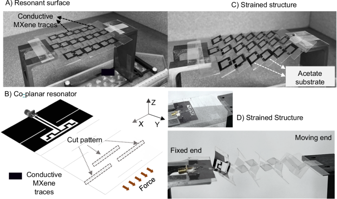
DISCUSSIONS MXENE-PATTERNED RECONFIGURABLE KIRIGAMI RESONANT SURFACE To demonstrate the feasibility of MXene patterning for manipulating incident electromagnetic waves, a two-dimensional
array (Fig. 1A) of split ring resonators was implemented from a water-based Ti3C2T_x_ solution. To maintain the physical size of the array within half the dimensions of an A4 paper, 105 mm ×
145 mm, and considering the frequency range of operation (the ISM band) for each split ring resonator, a layout of 19 SRRs was arranged and applied on the acetate substrate. The SRRs were
designed to establish electromagnetic coupling among the individual resonators51. The resonant frequency of the individual unit cells, _f__0_, was adjusted at 2.4 GHz, which was determined
by designing the physical length of the split rings (65 mm) to be approximately half of the corresponding wavelength (~λ0/2) at ~2.4 GHz. Further, the inter-element spacing of the resonant
array was optimized to improve the resonant profile quality by tuning the impedance matching between the resonant surface medium and free-space medium (Z0 ~ 377). To integrate the
MXene-based resonators on the flexible acetate substrates, MXene-based conductive traces were coated utilizing a Mayer rod coating method on the background-illuminated platform
(Supplementary Fig. 1). The MXene-based resonant surface and the carrying substrate were then cut in a Kirigami pattern to enable the microwave reconfigurability of the resonant frequency18.
Supplementary Fig. 2 shows the design dimensions for the Kirigami cut pattern and MXene-based split ring resonators. Figure 2B shows the measurement setup for investigating the microwave
strain sensitivity behavior of the MXene-patterned Kirigami sheet. The resonant surface was placed in the line of sight of an antenna, with centered alignment and at two distances of 19 cm
and 29 cm from the antenna. The antenna illuminated the electromagnetically-quiet chamber (details in the supplementary), where the reflected echo signals were processed52 to differentiate
resonant characteristics under varying strain states. Prior to evaluate the microwave performance of the MXene-patterned Kirigami reconfigurable resonant surface, the wireless test chamber,
mechanical holder, and the fabricated substrate with and without MXene patterning were electromagnetically characterized by measuring the reflection coefficient (S11 (dB)) of the
interrogator antenna (Fig. 2A). It was observed that placing the resonant surface disrupts wave propagation inside chamber, which is characterized by a (valley) notch response in the
measured spectra (2–3 GHz). This behavior was expected as placing an array of thin, electrically conductive (MXene-enabled) split-ring structures created a resonant medium with a
frequency-selective behavior53. Neither the empty chamber nor the chamber with the acetate substrate (no MXene patterning) showed indications of resonant behavior. The addition of the moving
stage and the acetate substrate increases the magnitude of the reflection coefficient to ~−30 dB; still, no indication of frequency-selective, resonant behavior is evident. Placing the
Kirigami-enabled, MXene-coated resonant surface resulted in a frequency-selective resonant surrounding (for the antenna), where multiple peaks and notches at 2.03 GHz, 2.35 GHz, 2.56 GHz,
2.81 GHz, and 2.97 GHz (in the range of 2–3 GHz) were observed. The observed notch at 2.56 GHz showed close proximity to the designed and simulated frequency of operation for MXene-based
SRRs. This resonant behavior of the array (i.e., surface) was resulted from individual ring resonator elements upon the incidence of external electromagnetic waves. The resonant performance
of MXene-based SRRs was simulated in ANSYS HFSS, and the results of Supplementary Fig. 4 shows the electric field intensity (E-field) distribution over split ring resonators with a dominant
resonant mode at 2.37 GHz. To demonstrate the capability of the proposed structure for monitoring strain, the MXene-patterned Kirigami resonant surface and the corresponding microwave
response were monitored for strain values ranging from 3% to 27%, and the results are shown in Fig. 2B. The deviating resonant frequencies (under strain) shown in Fig. 2B, establish a
characterization curve, relating sensitivity of resonant frequency to strain. The surface could detect 27% strain (Δ_L_/_L_) by demonstrating 202 MHz variation from the initial (unstrained
case) resonant frequency. Applying axial stress resulting in 27 % strain across the MXene-patterned Kirigami resonant surface showed a variation of 202 MHz compared to the case of 0% strain.
The measured normalized sensitivity showed a maximum of 18.3 MHz/(% strain) during experimentation, and the reported sensitivity was about 7 times higher than the sensitivity of Kirigami
SRRs reported in18. The minimum detectable strain was calculated based on the noise level and the resolution of the microwave instrument (i.e., IF bandwidth to be 0.3 kHz). However, due to
the mechanical limitations of the test setup, the minimum measured change in the resonant frequency was 63.3 MHz at 3% strain. The measurements were performed for a 3%-27% strain range,
observed on the resonant surface. These experiments were repeated for an antenna-to-array distance of 29 cm, and a similar trend was observed for the relation of resonant frequency versus
(%) strain values (Supplementary Fig. 5). The measured results of Fig. 2B were curve-fitted to a logistics function (with coefficients in the supplementary) that can model the exponential
increase in resonant frequency along with the saturation phase (for larger displacement) and minimum detection limit (for minute displacements). The predicted model indicated a 96%
correlation (similarity) with the experimentally extracted characterization curves. This observed trend for resonant frequency variations versus strain was consistent with the simulated
resonant behavior of the strained resonant surface in Fig. 2C, where displacing the unit cells decreased resonant frequency. This trend can be hypothetically tied to variations in the
inter-element and inter-unit cell coupling factors54 that cumulatively affected the resonant frequency of the entire surface for three-dimensional displacements. Figure 2D depicts the
modeled displacement and deflection of two SRRs (shown by black dashed lines from the side view) in ANSYS HFSS, in which the strain causes a separation between the adjacent SRRs and results
in rotation within their plane. The simulation results showed a deviation of approximately 350 MHz from the initial resonant frequency for displacements of 13% and 0% in ANSYS HFSS,
represented by the Δ_L_/_L_0 strain. Parametric and geometric studies of two electromagnetically coupled resonators in the HFSS simulation environment are presented in Supplementary Figs. 7,
8. The investigation was further extended to study the impact of the angle (θ1) of the incident wave on the MXene-based resonant surface, and the results are presented in Supplementary Fig.
8. Despite observing a dependency in the incident wave angle and the microwave response of the resonant surface, this will not impact the overall performance of the sensor system since the
angle impact can be nullified at the beginning of each measurement through baseline measurements. A parametric analysis utilizing Ansys HFSS was conducted to study the effect of MXene film
thickness on the microwave performance of the SRRs, with the results shown in Supplementary Figs. 9, 10. Examining the reflection coefficient reveals that the thickness of MXene SRRs (while
maintaining a conductivity constant at 10000 S cm−1) impacts their microwave performance, specifically in terms of microwave losses. An increase in the thickness enhances the resonance
quality, as indicated by the sharpness of notches and peaks with respect to a fixed frequency range. The marginal variations in notch and peak frequencies observed in the simulated spectra
for different thickness values can be explained by a change in the frequency at which “optimal impedance matching” occurs. This shift is merely an artifact of the mismatching between the
readout and resonator (MXene SRR) circuitry. Furthermore, the metallic conductivity of MXene allows the modeling of its electromagnetic characteristics as a thin film of a good
conductor54,55. Electromagnetic power may leak through thin conductors “after” they have penetrated and traveled within the conductive layer, resulting in additional power loss that may
degrade the quality factor of a resonant structure (such as the MXene-based SRRs), as opposed to altering the SRRs’ resonant frequency. A lumped element model analysis was performed to
further understand the structure’s microwave performance. The simulation results of a hypothetical circuit model showed a similar growth-saturation trend (as the Boltzmann function) for the
resonant frequency changes of strain states higher than 10% (Supplementary Fig. 11 shows the equivalent circuit model and the results). The finite conductivity of MXene-based resonators and
the electromagnetic coupling of adjacent elements were modeled using resistive, capacitive, and impedance-transforming elements using ANSYS Circuits. The resonant frequency showed a ~ 800
MHz shift for a 400% increase in the coupling factor. The growth and saturation trends depicted in Supplementary Fig. 9, Fig. 2B, C offer additional support for our methodology, which models
the sensitivity of inter-element electromagnetic coupling to mechanical displacements as a Boltzmann distribution. This distribution indicates that out-of-range reading values result from
relatively large or small displacements (scaled with the frequency of operation) at a fixed operating frequency (e.g., 2.4 GHz). The sensitivity of the resonant performance to Kirigami cut
pattern (size) variations was further evaluated, implementing a secondary array and the subsequent measurements (Supplementary Fig. 12), in which a correlation between mechanical
displaceability and sensor readings was noticed. Figure 3A illustrates an experimental study for investigating the functionality of MXene-based Kirigami sheet as a resonant surface with
mechanically reconfigurable scattering properties. In these experiments, a wireless channel was created between two (RX/TX: receiver/transmitter) antennas, and the MXene-based resonator
array served as a scattering surface with strain-adjustable characteristics (setup shown in Supplementary Fig. 3). To influence the beam direction of reflected waves from the surface, the
Kirigami structure was displaced using the moving stage. Figure 3B shows enabled changes in the scattering profile of the surface, resulting from the physical deflection and displacement of
the resonators. In this experiment, five different states (of strain) corresponding to Δ_L_ values of 0, 5, 10, 15, and 20 mm were considered (the measurements were repeated five times and
error bars represent standard deviation). The calculated strain values were 0%, 3.5%, 7%, 10%, and 13%, respectively. As demonstrated in Fig. 3B, as the strain values increased, the received
power at the second antenna, denoted by the magnitude of the transmission coefficient, _T_ (dB), exhibited an upward trend with an 8 dB increase for the 13% strain. The change in the
transmission coefficient (of the channel) was also observed in the spectral results of Supplementary Figs. 13, 14 from 2 to 8 GHz, showcasing a scattering profile of the surface and
redirecting more electromagnetic power to the receiver antenna. In addition, the ability to change the phase values of the complex transmission coefficient (_T_) under various strain states
is shown in Supplementary Fig. 14B, indicating that the resonant surface can function as a reconfigurable _delay_ mechanism for manipulating the wireless channel between two antennas. To
further investigate the adjustable scattering characteristics of the resonant surface, a simulated radar cross section (RCS) analysis was performed in ANSYS HFSS (see details in
Supplementary Information), as shown by Fig. 3C. This analysis is often used as a measure to characterize the scattering (or reflection) behavior of an object upon the incidence of
electromagnetic waves54. This analysis was performed for deflections of 0°, 15°, 30°, and 45°, resulting in beam tilts of 0°, 4°, 12°, and 24° for the reflected waves, respectively,
indicating that the deflection of SRRs from their plane, also tilts the direction of scattered waves, since the SRRs can be regarded as spatially displaced scatterers in this
experimentation. The simulation results of the reconfigurability of the radar cross section using mechanical displacements confirmed the measured observations on the adjustable manipulations
of the wireless channel between the two antennas (Fig. 4A). The experiments of the array’s adjustable scattering were repeated with a different arrangement of antennas and the array in the
chamber shown in Supplementary Fig. 14. Similarly, the transmission coefficient was measured and plotted versus different strain states of the array. States 1, 2, 3, 4, and 5 correspond 0%,
7%, 14%, 21%, and 28% strain (_Δl/L__0_), respectively. The measured deflections corresponding 0%, 7%, 14%, 21%, and 28% strain states were 0°, 11°, 18°, 30°, and 48°, respectively. It was
observed that among various states, state 3, causing an 18° deflection of the cells, resulted in a maximum power transfer scenario, showing the highest received signal strength of −34 dB.
States 2 and 4, each with the received signal strengths of −44 dB and −43 dB, demonstrated reduced transmission of electromagnetic power in the ASA configuration. The observed enhancement of
the signal transmission in the ASA configuration is attributed to the tunable reflectivity of the Kirigami resonant surface under different strain states. The deflection of each resonant
unit cell, and the array of resonators as a unified reflector, reshapes and tilts the beam of the reflected waves, consequently causing a tunable, strain-induced reflection profile.
MXENE-PATTERNED, KIRIGAMI-INSPIRED, CO-PLANAR RESONATOR As shown by Fig. 1B, a microwave resonator was also developed utilizing a co-planar topology and a wired-excitation method, where
metal traces were replaced by MXene-based traces as conductive strips. A multi-resonant design technique was employed to achieve strain-induced tunability across a range of microwave
frequencies in S, C, and X bands (4–10 GHz). The structure was designed using mismatched λ/4 transmission lines with high impedance termination resonating at the fundamental, second, and
third temporal harmonics. The excitation and performance evaluation of strain sensitivity was performed by attaching an SMA connector to the substrate, as seen in Supplementary Fig. 15. This
figure also shows the displacements and deformations in MXene-based co-planar resonators when the structure has undergone a strain state. This figure further shows the meandered traces and
the coplanar waveguide (CPW) ground plane being displaced from their initial configuration, suggesting changes in the layout of conductive sections, which can alter the characteristics of
electromagnetic wave coupling and wave transmission in the structure. A detailed investigation of the resonant mechanism, as well as the strain sensitivity, was performed using ANSYS HFSS
and ANSYS Circuit simulations, with the results included in Supplementary Figs. 16–19. To showcase the strain-sensitivity of the co-planar MXene-based resonator, Fig. 4A shows the microwave
reflection coefficient (_S_11, dB) from 1 to 10 GHz (left panel) and an expanded 6–10 GHz range (right panel) for different strain values. Three resonant notches were observed at _f_1 ≈ 4
GHz_, f_2 ≈ 7 GHz and _f_3 ≈ 9 GHz from the _S_11 response, displacing the structure shifts _f_2 and _f_3, and changing the notch depth at _f_1. The three main resonance frequencies are
strain sensitive. This is advantageous because monitoring resonance frequency throughout a spectrum is a more robust measurement (compared to amplitude tracking) for sensor purposes. The
_S_11 (dB) results may indicate a negligible variation of _f_1 over frequency. Yet, it should be noted that logarithmic magnitude calculation can obscure this trend of _S_11 at _f_1.
Conversely, the results of Supplementary Fig. 18 show that a slight 2.7% strain changes the _S_11 phase, suggesting changes in the complex input impedance. Figure 4B depicts the measured
resonant frequencies at different strain values (measured through the changes of length due to the axial stress as shown in Fig. 1). As seen from these results, the resonator’s third
resonant frequency (_f_3) (blue in Fig. 2B) undergoes a ~400 MHz shift for 22% of strain. The largest observed shift in _f_2 reached the value of 195 MHz at the same strain level. Further,
the notch amplitude variation at _f__1_ was tracked and included in these results, with the right Y-axis representing the total change from the initial _S_11 notch amplitude (in dB). For a
22% strain value, the notch amplitude changed by 22 dB, equivalent to a 158% change from the reflection coefficient of the unstrained case. Figure 4C displays the contour plots for the
complex magnitudes of electric field intensities generated by simulating the MXene-based co-planar topology in ANSYS HFSS. Due to resonance, a standing wave behavior is observed by the
discontinuous distribution of E-field intensities, with peaks (high-intensity regions) and nodes (low-intensity regions) occurring along the geometry (e.g., at _f__1_). Furthermore, it is
worth noting that the distribution of these standing waves undergoes variations as the frequency of operation increases. These variations create a distinction between _f__3_ and _f__1_,
where _f__3_ > _f__1_, signifying the presence of higher-order resonant modes at comparatively higher frequencies. The conductivity of a 1.29 µm-thick MXene film which was coated
utilizing the rod coating technique, was approximately 106 S m−1 (104 S m−1). This value was obtained by correlating the thickness through measurements of surface profile (Supplementary Fig.
21) and sheet resistance (Supplementary Fig. 22) values that were obtained using a stylus profilometer and a 4-probe conductivity meter (details in the SI), respectively. To test the
coating adhesion on acetate substrates, two sets of experiments were devised and executed. The adhesion of the coating was evaluated in these experiments in two ways. First, by subjecting
the coating to stress via a vibration mechanism, as illustrated in Supplementary Fig. 23, which ran for 20 minutes; and secondly, by applying stress by bowing the MXene-coated substrate in
the configuration shown in Supplementary Fig. 24 for a count of 100 cycles. Our manuscript is supplemented by a brief video depicting the experiment utilizing automated mechanical vibrations
(see Video S1). The coated samples prior to and after the experiments are shown in Supplementary Fig. 25, where visual inspection did not reveal any detachment of the coatings. DISCUSSION
It was shown that the integration of MXene on a Kirigami-inspired, flexible designs can enable functionalities such as frequency selectivity accompanied by strain-related reconfigurability.
This was achieved due to the high electrical conductivity of MXene coatings. Applying mechanical stress to the Kirigami design on a thin, flexible substrate generated large displacements and
led to resonant frequency deviations. Our experimental results showed a distinct correlation between varying resonant frequencies and the modeled strain. These thin, low-profile, flexible,
and lightweight arrays of MXene-based conductive structures allow dual-functionality, namely a strain-enabled reconfigurability, with potential applications in soft robotics, human-machine
interactions, reconfigurable intelligent surfaces, and multi-functional flexible components in space missions. Moreover, the room-temperature manufacturing of those Kirigami devices is easy
and cost-efficient. From a comparison of the demonstrated MXene-based prototypes with the already reported prototypes in refs. 16,17,18,56,57 (Supplementary Table 1), relatively
straightforward fabrication at conditions. Moreover, MXenes are chemically tunable58, allowing extensive opportunities to optimize the coating process. Last, titanium, the key component of
Ti3C2T_x_, is an abundant element, and the material can be scaled up for wide practical use. The implementation of MXene-based Frequency-Selective Surface (FSS) structures through a low-cost
and straightforward methodology constitutes the principal innovation of this work. Additionally, strain sensing is demonstrated as a practical application scenario. Our primary objective
continues to be the progression and implementation of FSS technology based on MXene nanomaterials, wherein strain sensing is merely one of the numerous possible applications for such
components. METHODS TI3C2T_X_ MXENE SYNTHESIS AND CHARACTERIZATIONS Ti3C2T_x_ was produced using the mixed acid method59. Initially, 10 g of Ti3AlC2 MAX powder (Carbon-Ukraine) was gradually
introduced into an etching solution composed of 60 ml of deionized water, 20 ml of 49% HF (Acros Organics), and 120 ml of 12 M HCl (Alfa Aesar, 98.5%). To ensure complete etching, the
mixture was stirred on a hotplate at 300 rpm and at room temperature for 24 h. Post-etching, the resulting multilayer Ti3C2 was washed repeatedly with deionized water (10 minutes per cycle
with 3500 rpm centrifugation) until the pH reached 6. Precautions, proper HF gear and waste handling systems were necessary for conducting the aforementioned etching and washing steps.
Subsequently, the multilayer Ti3C2 was immersed in a solution of 10 g LiCl (Chem-Impex Int., 99.3%) dissolved in 200 ml of deionized water and stirred for 12–24 h at 300 rpm and 35 °C to
allow the delamination to happen. The solution was then washed with deionized water through 10-minute centrifugation cycles at 3500 rpm. The clear supernatant containing excess LiCl was
decanted after each cycle and replaced with fresh deionized water. Once the supernatant turned dark, the MXene solution underwent additional centrifugation at 3500 rpm for 1 h to remove any
remaining LiCl. The clear supernatant was then decanted, and deionized water was replenished. Then, 10-minute centrifugation cycles at 3500 rpm were performed, with all dark supernatant
being collected as single-layer MXene flakes. The collection process ended when the supernatant became transparent. The as-collected MXene dispersion was concentrated by high-speed
centrifugation at 10000 rpm for 20 min, and the clear supernatant was subsequently removed. The concentration of the MXene solution was measured by vacuum filtrating 1 mL of the solution and
weighing the resulting freestanding film after 24 h of bench drying, informing the MXene synthesis yield of about 60%. The MXene freestanding film was assessed for electrical conductivity,
yielding a value of 11312 S cm−1, thereby validating the quality of the synthesized MXene. The concentration of the MXene solution was adjusted through centrifugation and dilution to achieve
the target of 20 mg mL−1. Dynamic light scattering (DLS) measurements (Supplementary Fig. 20) were performed to obtain the size (~1 μm) of the synthesized single-layer Ti3C2T_x_ MXene
flakes. The zeta potential was measured to be −47 mV, providing a stable dispersion needed for effective, uniform rod coating. A freestanding film was fabricated by vacuum filtering a small
amount of the MXene dispersion, from which X-ray diffraction (XRD) and Raman spectroscopy were performed. Both results confirmed the successful synthesis of Ti3C2T_x_, as they were well
aligned with previously reported literature60. TI3C2T_X_ MXENE FILM: SURFACE PROFILE We analyzed the conductivity and thickness of MXene coatings on an acetate substrate and simulated a
range of thickness and conductivity values to accurately predict the conductive split ring resonators (Supplementary Figs. 8–10). The surface profile acquired from this series of experiments
using the DEKTAKXT Stylus Profiler is depicted in Supplementary Fig. 21. The mean coating thickness was computed to be 1.29 µm. The lack of uniformity in the coating can be attributed to
the constraints of our comparatively uncomplicated fabrication technique, the rod coating method. TI3C2T_X_ MXENE FILM: BULK CONDUCTIVITY ANALYSIS The MXene patch (coating) was fabricated
using a rod dispersing a MXene solution with an average of 1460 nm in size distribution. The conductivity values (Supplementary Fig. 22) were extracted from the sheet resistance values
measured using Jandel’s cylindrical ResTest Four Point Probe System, and according to the below relation describing bulk conductivity of material body with square (L/W) cross section.
$$R=\frac{1}{\sigma t}\cdot \frac{L}{W}$$ (1) where _σ_ is the bulk conductivity of the MXene coating (unit: S m−1), and _L_, _W_, and _t_, are the length, width, and the thickness of
coating, respectively (unit: m). MICROWAVE INSTRUMENTATION A Keysight N5222B (200 MHz-26 GHz) Vector Network Analyzer (VNA) was used to measure the MXene-based structures scattering
parameters (S-parameters). The microwave measurements were performed with IF bandwidth and total sweep points set to 300 Hz and 4001 sweeping points, respectively. EXCITATION OF THE RESONANT
SURFACE WITH INCIDENT WAVES A broadband horn antenna (LB-20-180) from A-info was used as an illumination source and the receiver for the resonant surface excited by incident electromagnetic
waves. ELECTROMAGNETICALLY-QUIET CHAMBER The microwave measurements were performed in an electromagnetically-quiet chamber formed by AN-79 microwave absorber foams capable of absorbing
microwave signals from 900 MHz to 26 GHz. PROCESSING OF ANTENNA’S REFLECTION COEFFICIENT MEASUREMENTS FOR STRAIN EXPERIMENTS Single antenna measurements of a frequency selective array,
although in a quiet chamber, require a de-embedding procedure to nullify the effect of multiple reflections and fading in the channel. For this, a similar approach to experiments described
in ref. 52 was used, in which the de-embedded reflection coefficient of the resonant surface was calculated from: $$\Gamma ^{\prime}=\frac{\Gamma -{\Gamma }_{ant}}{1-\Gamma {\Gamma
}_{ant}}$$ (2) where \(\Gamma\) and \({\Gamma }_{{ant}}\) are the measured complex reflection coefficients of the channel with and without the resonant surface, and \(\Gamma ^{\prime}\) is
the de-embedded value which was considered as the spectral response for showing the changes of resonant frequency under strain. STRAIN CALCULATION The presented (%) strain values were
calculated by normalizing the length variation of the structures (\(\Delta l\)) to their initial unstrained length (\({l}_{0}\)). MASK PATTERNING FOR ACETATE SUBSTRATES During the MXene
coating process, adhesive masks made of patterned vinyl were utilized to cover the surface of the ACETATE substrate. The masks were patterned utilizing a Cricut Maker 3 machine, whereby the
areas to be coated were selectively removed. ACETATE SUBSTRATES Clear Cricut TM Acetate sheets61 were used as flexible substrates for coating MXene. MXENE COATING OF ACETATE SUBSTRATES After
creating a patterned mask on the acetate substrates, the thin sheet was plasma etched for three minutes to clean and functionalize the surface for enhanced MXene adhesion. MXene was then
subsequently coated on the substrate from a Ti3C2T_x_ colloidal solution (20 mg mL−1 in water). Rod coating (Supplementary Fig. 1) was used to produce a Ti3C2T_x_ MXene film on an acetate
substrate under ambient conditions. As shown in Fig. 1 in the manuscript, two resonant microwave structures, a microwave resonator component with co-planar excitation (wired) and a microwave
Kirigami resonant surface (sheet) were developed and evaluated for strain sensing and reconfigurable microwave properties. Displacement values were divided by the initial length of the
structure to present the measurements as a function of strain. Supplementary Fig. 1 and Fig. 1 of the manuscript also show the moving stage causing axial stress on the Kirigami cut patterned
substrate, coated with MXene. APPLYING KIRIGAMI CUT PATTERN A Cricut Maker 3, craft cutter machine was used to cut the MXene-coated acetate substrate in a Kirigami pattern, similar to the
pattern used in ref. 18. PROTOTYPE DIMENSIONS The MXene based Kirigami resonant surface (\(145{mm}\times 105{mm}\)) The MXene based Kirigami coplanar resonator (\(100{mm}\times 65{mm}\))
MOVING STAGE FOR INDUCING KIRIGAMI DISPLACEMENTS AND STRAIN RESPONSE The fixed and moving arms of the moving stage were additively manufactured using a PA12 nylon filament. The arms were
then assembled onto a fixed Plexiglass platform to enable the movement of one arm with respect to the other arm. Characterizing resonant parameters due to various strain values requires
steady displacement measurements using a designed test setup. In this work, a static horizontal strain was applied by extending a moving stage along the rail, which in turn rotates and bends
each row as strain increases. The maximum temporary deformation of the structure depends on the cut length, row size, and thickness of the material. Unless the structure is permanently
damaged by applying too much strain, it reverts to its original shape as the stress is removed. SIMULATIONS OF THE MXENE RESONATOR (FULL WAVE FREQUENCY RESPONSE) Full-wave electromagnetic
(FEM) simulations were performed using ANSYS HFSS (2023 R2) to derive the frequency response of the single port (wired) MXene-based resonator. The MXene layer was modeled as a finite
conductivity boundary on top of the ACETATE substrate with predefined dielectric properties. The assigned conductivity/length value for MXene parts was 5000 (S cm−1), and the thickness of
the MXene layer was assumed to be 10 µm. SIMULATIONS OF THE MXENE RESONATOR (CIRCUIT MODEL SIMULATIONS) ANSYS circuit (2023 R2) was used to perform circuit model simulations of the
multi-resonant MXene-based structure. The equivalent model (Supplementary Fig. 14) was developed utilizing transmission line elements and lumped elements to explain the resonant mechanism.
SIMULATIONS OF THE RESONANT SURFACE (UNIT CELL) Full-wave electromagnetic (FEM) simulations were performed using ANSYS HFSS to excite the unit cell of the resonant surface using an incident
plane wave using Master/Slave boundary conditions. This modeling assumed an infinite periodic array of resonators that were positioned in the transverse (X-Y) plane. The excitation of the
unit cell was conducted using a Floquet port along Z direction. SIMULATIONS OF THE RESONANT SURFACE (RADAR CROSS SECTION) Full-wave electromagnetic (FEM) simulations were performed using
ANSYS HFSS to excite the unit cell of the resonant surface using an incident plane wave with varying frequencies, and the RCS of the structure was extracted in the post-processing of the
scattered fields. CURVE FITTING OF MEASUREMENT FOR STRAIN-SENSITIVITY The measurements of Fig. 2B in the manuscript were curve fitted to a logistics exponential function with the following
equation and _R_2 of 96%: $$y={A}_{2}+\frac{{A}_{1}-{A}_{2}}{1+{(\frac{x}{{x}_{0}})}^{p}}$$ (3) where \({A}_{2}=197.5,{A}_{1}=1.7,p=1.96,{x}_{0}=5.29\). KIRIGAMI CUT PATTERN AND DIMENSIONS
To further demonstrate the versatility of the MXene-based reconfigurable surface, two Kirigami cuts with different dimensions and the trace width of split ring resonators were implemented.
The resonant array with thinner MXene traces for SRRs and longer Kirigami cuts was found to be highly sensitive to mechanical forces and gravitational pull, leading to inconsistent and
unrepeatable readings for strain sensing experiments. The results of this implementation are provided in Supplementary Fig. 10. This experiment showed that the Kirigami displacements are
design-dependent, and the reconfigurability and repeatable strain sensing performance are influenced by the dimensions of the cut pattern. OPERATION PRINCIPLES OF THE CO-PLANAR RESONATOR
Supplementary Fig. 14 illustrates the primary resonant parts (the slot and the co-planar resonator) of this multi-frequency design. The resonator consists of two lossy λ/4 TLs and a
CPW-based slot resonator, where changing the electrical length of the transmission lines affects resonant characteristics. The electrical length of the CPW TL, \(\theta\), can be expressed
by ref. 62: $$\theta ^\circ=\beta d=\frac{\omega \sqrt{(1+{\varepsilon }_{r})/2}}{c}d$$ (4) where _ε__r_ is the relative permittivity of the medium under the CPW layer, \(\omega\) is the
frequency, _c_ is the speed of light in the vacuum, and _d_ is the physical length of the TL. This permittivity value can be considered ~1, as the thickness of the substrate (~0.1 mm) is
almost ten times smaller than the width of the signal trace. An equivalent circuit model utilizing transmission line theory and lumped elements was adopted to explain the resonant mechanism
(Supplementary Fig. 14). As illustrated, the resonance behavior mainly results from a TL divider (a lossy power divider) and a rectangular slot created in the CPW ground. The two meandered
lossy TLs terminated in a high impedance and an _RLC_ tank that represents the slot’s resonance. In addition, Supplementary Fig. 14 summarizes the corresponding values of the selected TL
model, where _R__s_, _L__s_, and _C__s_, represent the slot’s _RLC_ resonance. The effect of the meandered geometry of the TLs is modeled by assigning an imaginary part to the load
impedance, _Z_L. To further investigate the resonant behavior, the real and imaginary parts of the resonator’s input impedance (_Z_11) were simulated in ANSYS HFSS with the results shown in
Supplementary Fig. 15. The results indicate that the electromagnetic coupling of TLs and slot resonator creates three resonances at ~ _n_λ/4 (_n_ is 1, 2, 3) frequencies of the TLs. By
monitoring the peak Re (_Z_11) and zero crossing of _Im_ (_Z_11) in the 1–10 GHz range, three resonances near 3.5 GHz, 6.5 GHz, and 9.3 GHz are seen. It is anticipated that changing the
geometrical arrangement of the TLs and the co-planar ground will change the electromagnetic couplings within the resonator, leading to variations in the resonant frequency of the sensor.
Supplementary Fig. 17 shows the simulated results for S11 of the resonator, both for ANSYS HFSS and ANSYS Circuits (Supplementary Fig. 15) models, where the reflection coefficient is
calculated from the start of the main ~(λ/4) CPW feed line. These results indicate that the feed line can successfully match the input impedance of the resonator (_Z_11) to a standard 50 Ω
impedance at the proximity of previously mentioned resonant frequencies (~3.5 GHz, ~6.5 GHz, and 9.3 GHz). An additional impedance matching, occurring at ~4.5 GHz is observed, which can be
explained by referring to Supplementary Fig. 15 and noting that the impedance at this frequency approaches a pure real value. The results of circuit model simulations and the full-wave
simulations show good consistency, indicating that the selected equivalent model can adequately explain the resonant mechanism and the tunability of the designed geometry. Supplementary Fig.
17 further shows the measured S11 of the fabricated coplanar resonator structure with a Kirigami cut pattern and the simulated S11 of the 3D modeled resonator with the same cuts. The
simulated and measured results demonstrate excellent consistency, showing matching resonances around the expected frequencies. The slight variations between the simulated and measured
results can be related to fabrication imperfections, such as the homogeneity of the coating and the generation of evanescent modes at the junction of the SMA connector and conductive MXene
coating. DATA AVAILABILITY The data supporting the findings of the study are included in the main text and supplementary information files. Source data are provided with this paper.
REFERENCES * Pan, C. et al. Reconfigurable intelligent surfaces for 6G systems: Principles, applications, and research directions. _IEEE Commun. Mag._ 59, 14–20 (2021). Article Google
Scholar * ElMossallamy, M. A. et al. Reconfigurable intelligent surfaces for wireless communications: principles, challenges, and opportunities. _IEEE Trans. Cogn. Commun. Netw._ 6,
990–1002 (2020). Article Google Scholar * Cao, Z., Li, Y., Zhang, Z. & Iskander, M. F. Single motor-controlled mechanically reconfigurable reflectarray. _IEEE Trans. Antennas Propag._
71, 190–199 (2023). Article ADS Google Scholar * Wang, R., Han, L., Wu, C., Dong, Y. & Zhao, X. Localizable, identifiable, and perceptive untethered light-driven soft crawling robot.
_ACS Appl. Mater. Interfaces_ 14, 6138–6147 (2022). Article CAS PubMed Google Scholar * Wang, C. et al. Pangolin-inspired stretchable, microwave-invisible metascale. _Adv. Mater._ 33,
2102131 (2021). Article CAS Google Scholar * Aziz, S. et al. A microwave powered polymeric artificial muscle. _Appl. Mater. Today_ 23, 101021 (2021). Article Google Scholar * Fok, M.,
Liu, Q. & Yang, M. Biomimicry in Microwave Photonics and Soft Robotic with Fiber Optics Sensors. in _2022_ _IEEE International Topical Meeting on Microwave Photonics, MWP 2022 -
Proceedings_ (IEEE, Orlando, FL, USA, 2022). * Shah, S. I. H., Sarkar, A. & Lim, S. Electromechanically deployable high-gain pop-up antenna using shape memory alloy and kirigami
technology. _IEEE Access_ 8, 225210–225218 (2020). Article Google Scholar * Wang, H. et al. Origami–kirigami arts: Achieving circular dichroism by flexible meta-film for electromagnetic
information encryption. _Laser Photonics Rev._ 17, 2200545 (2023). Article ADS Google Scholar * Charkhabi, S. et al. Kirigami-enabled, passive resonant sensors for wireless deformation
monitoring. _Adv. Mater. Technol._ 4, 1800683 (2019). Article Google Scholar * Zhang, J., Miao, W., Zhang, L. & Wang, C. Kirigami-based stretchable low-radar-cross-section microstrip
antenna: Design and analysis. _AIAA J._ 60, 1958–1964 (2022). Article ADS Google Scholar * Cui, Y., Nauroze, S. A., Bahr, R. & Tentzeris, E. M. 3D printed one-shot deployable flexible
‘kirigami’ dielectric reflectarray antenna for mm-wave applications. In _IEEE MTT-S International Microwave Symposium Digest_ (IEEE, Los Angeles, CA, USA, 2020). * Khosravi, H. & Li, S.
Tunable wave-propagation band gap via stretching Kirigami sheets. _Phys. Rev. Appl._ 17, 064054 (2022). Article ADS CAS Google Scholar * Lamoureux, A., Lee, K., Shlian, M., Forrest, S.
R. & Shtein, M. Dynamic kirigami structures for integrated solar tracking. _Nat. Commun._ 6, 8092 (2015). Article ADS PubMed Google Scholar * Liu, J. et al. Self-healing kirigami
assembly strategy for conformal electronics. _Adv. Funct. Mater._ 32, 2109214 (2022). Article CAS Google Scholar * Baghelani, M., Abbasi, Z. & Daneshmand, M. High-dynamic-range
chipless microwave resonator-based strain sensor. _IEEE Trans. Instrum. Meas._ 70, 1–7 (2021). Google Scholar * Wang, L., Chung, K. L., Zong, W. & Feng, B. A highly sensitive microwave
patch sensor for multidirectional strain sensing based on near orthogonal modes. _IEEE Access_ 9, 24669–24681 (2021). Article Google Scholar * Dijvejin, Z. A., Kazemi, K. K., Alasvand
Zarasvand, K., Zarifi, M. H. & Golovin, K. Kirigami-enabled microwave resonator arrays for wireless, flexible, passive strain sensing. _ACS Appl. Mater. Interfaces_ 12, 44256–44264
(2020). Article CAS PubMed Google Scholar * Hegde, M. et al. 3D printing all-aromatic polyimides using mask-projection stereolithography: processing the nonprocessable. _Adv. Mater._ 29,
1701240 (2017). Article Google Scholar * Shi, Q. et al. Substrate developments for the chemical vapor deposition synthesis of graphene. _Adv. Mater. Interfaces_ 7, 1902024 (2020). Article
CAS Google Scholar * Melentiev, R., Yudhanto, A., Tao, R., Vuchkov, T. & Lubineau, G. Metallization of polymers and composites: State-of-the-art approaches. _Mater. Des._ 221, 110958
(2022). Article CAS Google Scholar * Bello, M. & Shanmugan, S. Achievements in mid and high-temperature selective absorber coatings by physical vapor deposition (PVD) for solar
thermal Application-A review. _J. Alloy. Compd._ 839, 155510 (2020). Article CAS Google Scholar * Matthews, A., Leyland, A. & Stevenson, P. Widening the market for advanced PVD
coatings. _J. Mater. Process. Technol._ 56, 757–764 (1996). Article Google Scholar * Bobzin, K., Brögelmann, T. & Kruppe, N. C. Enhanced PVD process control by online substrate
temperature measurement. _Surf. Coat. Technol._ 354, 383–389 (2018). Article CAS Google Scholar * Boholm, M. & Arvidsson, R. Controversy over antibacterial silver: Implications for
environmental and sustainability assessments. _J. Clean. Prod._ 68, 135–143 (2014). Article CAS PubMed Google Scholar * Iijima, S. Helical microtubules of graphitic carbon. _Nature_ 354,
56–58 (1991). Article ADS CAS Google Scholar * Orts Mercadillo, V. et al. Electrically conductive 2D material coatings for flexible and stretchable electronics: A comparative review of
Graphenes and MXenes. _Adv. Funct. Mater._ 32, 2204772 (2022). Article CAS Google Scholar * Dragoman, M. et al. Coplanar waveguide on graphene in the range 40 MHz-110 GHz. _Appl. Phys.
Lett._ 99, 033112 (2011). Article ADS Google Scholar * Kang, T. G. et al. Microwave characterization of conducting polymer PEDOT: PSS film using a microstrip line for humidity sensor
application. _Meas. J. Int. Meas. Confed._ 137, 272–277 (2019). Article Google Scholar * Saib, A. et al. Carbon nanotube composites for broadband microwave absorbing materials. _IEEE
Trans. Microw. Theory Tech._ 54, 2745–2753 (2006). Article ADS CAS Google Scholar * Srivastava, S. K. & Manna, K. Recent advancements in the electromagnetic interference shielding
performance of nanostructured materials and their nanocomposites: a review. _J. Mater. Chem. A_ 10, 7431–7496 (2022). Article CAS Google Scholar * Wang, X. X., Cao, W. Q., Cao, M. S.
& Yuan, J. Assembling nano–microarchitecture for electromagnetic absorbers and smart devices. _Adv. Mater._ 32, 2002112 (2020). Article CAS Google Scholar * Ghivela, G. C. &
Sengupta, J. The promise of Graphene: a survey of microwave devices based on Graphene. _IEEE Microw. Mag._ 21, 48–65 (2020). Article Google Scholar * Park, J. G. et al. Electromagnetic
interference shielding properties of carbon nanotube buckypaper composites. _Nanotechnology_ 20, 415702 (2009). Article PubMed Google Scholar * Mirri, F. et al. Lightweight, flexible,
high-performance carbon nanotube cables made by scalable flow coating. _ACS Appl. Mater. Interfaces_ 8, 4903–4910 (2016). Article CAS PubMed Google Scholar * Dadashi Firouzjaei, M.,
Karimiziarani, M., Moradkhani, H., Elliott, M. & Anasori, B. MXenes: The two-dimensional influencers. _Mater. Today Adv._ 13, 100202 (2022). Article CAS Google Scholar * Hart, J. L.
et al. Control of MXenes’ electronic properties through termination and intercalation. _Nat. Commun._ 10, 522 (2019). Article ADS CAS PubMed PubMed Central Google Scholar * Anasori, B.
et al. Control of electronic properties of 2D carbides (MXenes) by manipulating their transition metal layers. _Nanoscale Horiz._ 1, 227–234 (2016). Article ADS CAS PubMed Google
Scholar * Sarycheva, A. et al. 2D titanium carbide (MXene) for wireless communication. _Sci. Adv._ 4, eaau0920 (2018). Article ADS PubMed PubMed Central Google Scholar * Khorsand
Kazemi, K. et al. MXene membrane in planar microwave resonant structures for 5G applications. _Appl. Mater. Today_ 26, 101294 (2022). Article Google Scholar * Huang, W., Hu, L., Tang, Y.,
Xie, Z. & Zhang, H. Recent advances in functional 2D MXene-based nanostructures for next-generation devices. _Adv. Funct. Mater._ 30, 2005223 (2020). Article CAS Google Scholar * Yan,
J. et al. Flexible MXene/Graphene films for ultrafast supercapacitors with outstanding volumetric capacitance. _Adv. Funct. Mater._ 27, 1701264 (2017). * Li, G. et al. 2D titanium carbide
(MXene) based films: Expanding the frontier of functional film materials. _Adv. Funct. Mater._ 31, 2105043 (2021). Article CAS Google Scholar * Ma, C., Ma, M. G., Si, C., Ji, X. X. &
Wan, P. Flexible MXene-based composites for wearable devices. _Adv. Funct. Mater._ 31, 2009524 (2021). Article CAS Google Scholar * Mathis, T. S. et al. Modified MAX phase synthesis for
environmentally stable and highly conductive Ti3C2 MXene. _ACS Nano_ 15, 6420–6429 (2021). Article CAS PubMed Google Scholar * Niksan, O., Wyatt, B. C., Kazemi, K. K., Anasori, B. &
Zarifi, M. H. MXene free standing films: unlocking the impact of flake sizes in microwave resonant structures in humid environments. _Small_ 19, 2300848 (2023) * Khorsand Kazemi, K. et al.
Low-profile planar antenna sensor based on Ti3C2Tx MXene membrane for VOC and humidity monitoring. _Adv. Mater. Interfaces_ 9, 2102411 (2022). Article CAS Google Scholar * Pei, Y. et al.
Ti3C2TX MXene for sensing applications: Recent progress, design principles, and future perspectives. _ACS Nano_ 15, 3996–4017 (2021). Article CAS PubMed Google Scholar * Lipatov, A. et
al. Elastic properties of 2D Ti3C2TX MXene monolayers and bilayers. _Sci. Adv._ 4, eaat0491 (2018). Article ADS PubMed PubMed Central Google Scholar * Han, M. et al. Beyond Ti3C2TX:
MXenes for electromagnetic interference shielding. _ACS Nano_ 14, 5008–5016 (2020). Article CAS PubMed Google Scholar * Niksan, O., Colegrave, K. & Zarifi, M. H. Battery-free,
artificial neural network-assisted microwave resonator array for ice detection. _IEEE Trans. Microw. Theory Tech._ 71, 698–709 (2023). Article ADS Google Scholar * Maleki Gargari, A.,
Zarifi, M. H. & Markley, L. Passive matched mushroom structure for a high sensitivity low profile antenna-based material detection system. _IEEE Sens. J._ 19, 6154–6162 (2019). Article
ADS Google Scholar * Pendry, J. B., Holden, A. J., Robbins, D. J. & Stewart, W. J. Magnetism from conductors and enhanced nonlinear phenomena. _IEEE Trans. Microw. Theory Tech._ 47,
2075–2084 (1999). Article ADS Google Scholar * Pozar, D. M. Microwave Engineering, 4th Ed. _John Wiley &Sons, Inc_ (Wiley, 2012). * Han, M. & Gogotsi, Y. Perspectives for
electromagnetic radiation protection with MXenes. _Carbon N. Y._ 204, 17–25 (2023). Article CAS Google Scholar * Tang, Y., Chen, Y., Zhang, Q., Shi, B. & Huang, J. Enhanced
sensitivity and robustness in an embeddable strain sensor using microwave resonators. _IEEE Trans. Instrum. Meas._ 73, 1–8 (2024). Google Scholar * Cheng, S. & Wu, Z. A microfluidic,
reversibly stretchable, large-area wireless strain sensor. _Adv. Funct. Mater._ 21, 2282–2290 (2011). Article CAS Google Scholar * Mohammadi, A. V., Rosen, J. & Gogotsi, Y. The world
of two-dimensional carbides and nitrides (MXenes). _Science_ 80, 372 (2021). Google Scholar * Shuck, C. E. et al. Scalable synthesis of Ti3C2Tx. _Adv. Eng. Mater._ 22, 539–560 (2020).
Article Google Scholar * Shekhirev, M., Shuck, C. E., Sarycheva, A. & Gogotsi, Y. Characterization of MXenes at every step, from their precursors to single flakes and assembled films.
_Prog. Mater. Sci_. 120, 100757 (2021). * Acetate Sheets 12” x 12”, Clear. https://cricut.com/en-ca/materials/material-type/specialty/foil-acetate/acetate-sheets-12-x-12-clear/2003600.html.
* Wen, C. P. Coplanar waveguide: a surface strip transmission line suitable for nonreciprocal gyromagnetic device applications. _IEEE Trans. Microw. Theory Tech._ 17, 1087–1090 (1969).
Article ADS Google Scholar Download references ACKNOWLEDGEMENTS UBC-affiliated authors would like to recognize the Syilx Okanagan Nation for using their unceded territory, the land on
which this research was conducted. The authors thank Aaryaman Shah for the fabrication of the moving stage. UBC authors thank the Department of National Defense for supporting this work
under Contract W7714-228359 and the support from the Natural Sciences and Engineering Research Council of Canada (NSERC), through grant RGPIN-2018-04288 and the Canadian Foundation for
Innovation (CFI) through grant no. 38148 and 37904. They would also like to thank Rogers Corporation for supplying microwave substrates and CMC Microsystems for their support in the form of
software access and equipment. MXenes development at Drexel University was supported by the U.S. National Science Foundation grant DMR-2041050. AUTHOR INFORMATION AUTHORS AND AFFILIATIONS *
School of Engineering, Faculty of Applied Sciences, University of British Columbia, Kelowna, BC, V1V 1V7, Canada Omid Niksan & Mohammad H. Zarifi * Department of Materials Science and
Engineering and A. J. Drexel Nanomaterials Institute, Drexel University, Philadelphia, PA, 19104, USA Lingyi Bi & Yury Gogotsi Authors * Omid Niksan View author publications You can also
search for this author inPubMed Google Scholar * Lingyi Bi View author publications You can also search for this author inPubMed Google Scholar * Yury Gogotsi View author publications You
can also search for this author inPubMed Google Scholar * Mohammad H. Zarifi View author publications You can also search for this author inPubMed Google Scholar CONTRIBUTIONS Omid Niksan
performed the design, fabrication, and experimental/numerical (simulative) investigations of the demonstrated frequency selective components. He was the primary writer of the manuscript.
Lingyi Bi conducted experiments, analyzed the experimental data, participated in the discussion on the results, and edited the manuscript. Yury Gogotsi edited the manuscript, supervised, and
directed the project. Mohammad H. Zarifi performed conceptualization, formal analysis, investigation, methodology, project administration, supervision, validation, writing original draft,
writing review & editing, as well as securing funding for the project. CORRESPONDING AUTHORS Correspondence to Yury Gogotsi or Mohammad H. Zarifi. ETHICS DECLARATIONS COMPETING INTERESTS
The authors declare no competing interests. PEER REVIEW PEER REVIEW INFORMATION _Nature Communications_ thanks Sang Ouk Kim and the other, anonymous, reviewer for their contribution to the
peer review of this work. A peer review file is available. ADDITIONAL INFORMATION PUBLISHER’S NOTE Springer Nature remains neutral with regard to jurisdictional claims in published maps and
institutional affiliations. SUPPLEMENTARY INFORMATION SUPPLEMENTARY INFORMATION PEER REVIEW FILE SOURCE DATA SOURCE DATA RIGHTS AND PERMISSIONS OPEN ACCESS This article is licensed under a
Creative Commons Attribution-NonCommercial-NoDerivatives 4.0 International License, which permits any non-commercial use, sharing, distribution and reproduction in any medium or format, as
long as you give appropriate credit to the original author(s) and the source, provide a link to the Creative Commons licence, and indicate if you modified the licensed material. You do not
have permission under this licence to share adapted material derived from this article or parts of it. The images or other third party material in this article are included in the article’s
Creative Commons licence, unless indicated otherwise in a credit line to the material. If material is not included in the article’s Creative Commons licence and your intended use is not
permitted by statutory regulation or exceeds the permitted use, you will need to obtain permission directly from the copyright holder. To view a copy of this licence, visit
http://creativecommons.org/licenses/by-nc-nd/4.0/. Reprints and permissions ABOUT THIS ARTICLE CITE THIS ARTICLE Niksan, O., Bi, L., Gogotsi, Y. _et al._ MXene-based kirigami designs:
showcasing reconfigurable frequency selectivity in microwave regime. _Nat Commun_ 15, 7793 (2024). https://doi.org/10.1038/s41467-024-51853-1 Download citation * Received: 28 February 2024 *
Accepted: 20 August 2024 * Published: 06 September 2024 * DOI: https://doi.org/10.1038/s41467-024-51853-1 SHARE THIS ARTICLE Anyone you share the following link with will be able to read
this content: Get shareable link Sorry, a shareable link is not currently available for this article. Copy to clipboard Provided by the Springer Nature SharedIt content-sharing initiative