- Select a language for the TTS:
- UK English Female
- UK English Male
- US English Female
- US English Male
- Australian Female
- Australian Male
- Language selected: (auto detect) - EN
Play all audios:
ABSTRACT A clock distribution network (CDN) is a ubiquitous on-chip element that provides synchronized clock signals to all different circuit blocks in the chip. To maximize the chip
performance, today’s CDN demands lower jitter, skew, and heat dissipation. Conventionally, on-chip clock signals have been distributed in the electric voltage domain, resulting in increased
jitter, skew, and heat dissipation due to clock drivers. While low-jitter optical pulses have been locally injected in the chip, research on effective distribution of such high-quality clock
signals has been relatively sparse. Here, we demonstrate femtosecond-precision distribution of electronic clocks using driver-less CDNs injected by photocurrent pulses extracted from an
optical frequency comb source. Femtosecond-level on-chip jitter and skew can be achieved for gigahertz-rate clocking of CMOS chips by combining ultralow comb-jitter, multiple driver-less
metal-meshes, and active skew control. This work shows the potential of optical frequency combs for distributing high-quality clock signals inside high-performance integrated circuits,
including 3D integrated circuits. SIMILAR CONTENT BEING VIEWED BY OTHERS PHOTONIC CHIP-BASED LOW-NOISE MICROWAVE OSCILLATOR Article Open access 06 March 2024 ATTOSECOND ELECTRONIC TIMING
WITH RISING EDGES OF PHOTOCURRENT PULSES Article Open access 22 July 2020 A CHIP-INTEGRATED COMB-BASED MICROWAVE OSCILLATOR Article Open access 30 April 2025 INTRODUCTION In a
high-performance CMOS chip, well synchronized clock signals must be provided to all circuit elements by the CDN1,2,3. Conventionally, on-chip clock signals have been generated and
distributed via tree- or mesh-based networks in the electric voltage domain1,2,3,4,5. As electronic clock generators are unable to drive the clock load directly, many levels of clock drivers
have been employed to overcome the bandwidth limitations. Due to the large number of clock drivers in processors and digital systems, substantial power consumption occurs, accounting for
10–30% of overall chip power consumption6,7,8,9 and causing on-chip thermal problems. As each clock driver adds timing uncertainty, jitter (random variation in clock arrival time) and skew
(spatial variation in clock arrival time) performances are also significantly impaired. As a result, both jitter and skew performances have been limited to several to tens ps range1,5,8,10.
While the demand for higher data rates necessitates a tighter jitter and skew budget, clock skew and jitter deteriorate as on-chip process, voltage and temperature (PVT) variations worsen in
deep sub-micron processes. Optical pulse trains generated from femtosecond mode-locked lasers and optical frequency combs can provide intrinsically low timing jitter down to the
sub-100-attoseconds regime11,12. For this reason, they have been actively used for precise timing applications, including synchronization of large-scale X-ray free-electron lasers13,
high-speed photonic analogue-to-digital converters (ADCs)14 and photonics-based radars15, to name a few. Naturally, utilizing ultralow-jitter optical pulses in electronic or
electronic-photonic chips has also been actively investigated16,17,18,19,20,21,22,23. For the on-chip clocking, an early-stage pioneering experimental study employed ultrashort optical
pulses generated from an 80 MHz mode-locked Ti:sapphire laser to inject a local clock signal to a four-stage flip-flop with 5.9-ps timing jitter16, and later to a multiplexer down to 0.93-ps
jitter24. Directly injecting low-jitter optical pulses in the chip for optical sampling and ADCs was also investigated, showing that local pulse injection with tens-femtosecond-level
relative jitter (which is inferred from the measured signal-to-noise ratio of a converter) is possible21,23. While ultralow-jitter local clocks could have been injected and generated in the
chip, to our knowledge, there has been little study on the distribution of such clock signals with femtosecond precision inside the chip. Here, we demonstrate femtosecond-precision
distribution of electronic clock signals inside a CMOS chip using a driver-less CDN injected by photocurrent pulses. Our approach directly drives driver-less metal-mesh sections in a CMOS
chip by low-jitter, sharp-edged photocurrent pulses extracted from balanced photodiodes when illuminating them with optical pulse trains generated from an optical frequency comb source. On
the one hand, the use of low-jitter and ultrashort optical pulses11,12 generated from an optical frequency comb source can naturally reduce the timing jitter of the extracted electronic
clock signals in the CMOS chip. On the other hand, the use of ultrashort optical pulses for generating strong photocurrent pulses can remove the necessity of clock drivers in the CDN and,
therefore, can significantly reduce the skew and on-chip heat dissipation. By dividing the clock domains into multiple sections with driver-less metal structures, the CDN can be implemented
in a scalable way. The final inter-domain skews can be compensated by monitoring them with a ~ 100-fs-resolution on-chip time-to-digital converter (TDC)25 and sending the timing information
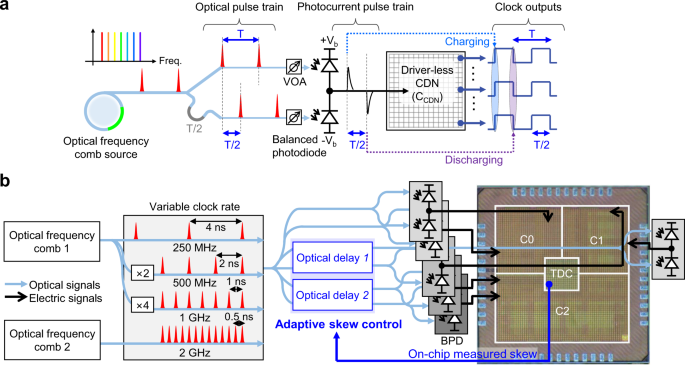
to the optical domain. RESULTS CONCEPT AND EXPERIMENTAL SETUP Figure 1a shows the conceptual schematic diagram of the demonstrated photonic CDN. The basic idea is to generate a clock signal
by charging and discharging the capacitive load (the global metal-mesh in the CMOS chip CCDN in Fig. 1a) by short photocurrent pulses with opposite polarity. While a demonstration of
injecting photocurrent pulses to a local capacitive load (with ~100 fF load26) has been shown16, our approach is different in that it injects the current pulses directly into the global
metal-mesh in the CMOS chip. The optical pulse train, with pulse repetition rate equivalent to the targeted clock rate, is split into two by a coupler. To create a 50% duty-cycle clock, one
path experiences a delay corresponding to half of the clock period (T/2 in Fig. 1a). The set of optical pulse trains is applied to an off-chip balanced photodiode. Variable optical
attenuators (VOAs in Fig. 1a) are inserted to compensate for the mismatch in photogenerated carriers caused by process variation of photodiodes, waveguide losses, and coupling ratio
imbalance in the optical coupler. The balanced photodiode converts optical pulses to low-jitter, high-peak, and short photocurrent pulses with opposite polarity, which can directly charge
and discharge the capacitance imposed by clock distribution structure and clock loads, generating lower-jitter and sharp clock edges in the voltage domain. Furthermore, by putting multiple
metal-mesh sections on a chip, it is possible to achieve not only scalability in drivable load but also efficient operation of different circuit blocks under various clock load conditions.
Figure 1b shows the schematic of the photonic CDN demonstration experiment. A mode-locked Er-fibre oscillator with a 250 MHz repetition rate is employed as an optical frequency comb source.
By interleaving the 250 MHz pulses with a two-stage fibre Mach-Zehnder interferometer-based pulse interleaver27, we were able to generate 500 MHz and 1 GHz optical pulse trains. We also used
a separate 2 GHz Er-waveguide laser to generate a clock signal up to 2 GHz rate. A test chip prototype is designed and fabricated in 65 nm CMOS process (the chip die photo shown in Fig.
1b). The test chip includes three driver-less clock distribution structures as a form of metal mesh, clamper circuits for protection, D-flipflop-based active loads, an H-tree-based CDN for
comparison, and a sub-ps-resolution stochastic TDC25 to measure skew (see Methods). Note that, in order to demonstrate scalability in drivable load and efficient operation of different
circuit blocks with different clock load conditions, we designed the chip with three separate clock domains (labelled as C0, C1 and C2 in Fig. 1b). Clock domains C1 and C2 consist of
additional dynamic clock loads (i.e., 6036 and 3360 D-flipflops, respectively) to study the impact of active loads. In addition, for comparison with conventional electronic CDN, an H-tree
structure with 23 stages of clock drivers (1194 in total) is placed under the C2 structure. The chip area is 2 mm by 2 mm, and the capacitance of each clock mesh plus clock load is 12.7 pF,
17.0 pF and 26.6 pF for C0, C1, and C2 clock domains, respectively, which are estimated with the parasitic extraction tool28. Note that adaptive skew control between different clock domains
can be also achieved by monitoring the inter-domain skew with the on-chip TDC and transmitting this information to the delay control actuator in the optical path. By applying optical pulses
to an off-chip 5-GHz balanced photodiode connected to the pad, current pulses are directly injected into each clock domain on the chip. Note that, to drive a larger clock load (for example,
C2 in Fig. 1b), multiple balanced photodiodes can be connected in parallel to increase the effective charges of photocurrent pulses. The on-chip clocks are fed out with one clock driver
followed by an open drain driver, while the clocks from the H-tree CDN are fed out with two stages of clock driver followed by an open drain driver. Figure 2 shows the measured waveforms of
the input photocurrent pulse trains and the generated CDN clock outputs when 250 MHz, 500 MHz, and 1 GHz optical pulse trains are applied to the C2 clock domain when the dynamic clock load
as well as the H-tree section are turned on (clock outputs with different clock rates and load conditions are presented in Supplementary Fig. 1). The clock output for 2 GHz optical pulse
train is also generated from the C0 clock domain. JITTER PERFORMANCE Figure 3a shows the system configuration showing the locations and elements related to the jitter measurement. The
on-chip clock at each clock domain is fed out from nodes denoted as red arrows in Fig. 3a with an open-drain clock driver for off-chip waveform and jitter measurement using an oscilloscope
(see Methods). Note that the trigger signal for the oscilloscope is provided by the photodetected signal of the optical pulse train, and the rms jitter measurement background is determined
to be ~350 fs rms (Fig. 3b). Since the edge of photocurrent pulses, which has fs-level jitter29, was used as the trigger signal (see Methods), we attribute this ~350-fs-level background
jitter to the instrument limit of the used oscilloscope30. The jitter measurement results of 1 GHz digital clock distributed through the photonic CDN and the conventional H-tree CDN are
presented in Fig. 3c–f. The clock signals extracted from the C0, C1 and C2 clock domains show rms jitter of 351 fs, 356 fs, and 389 fs, respectively (Fig. 3c–e), which implies that the
current jitter measurements are limited by the instrument noise of the used oscilloscope and the actual jitter in the photonic CDN is much lower. Any noticeable difference in timing jitter
is not observed according to various clock load conditions within the same clock domain (see Supplementary Fig. 2). On the other hand, the conventional H-tree CDN shows significantly higher
rms timing jitter of ~2.5 ps (Fig. 3f). Because the frequency comb’s timing jitter and the optical-to-electronic conversion jitter are both known to be significantly lower, the CDN jitter
directly from the clock mesh might also be much lower than the oscilloscope’s instrument limit (350 fs). To investigate the actual jitter, we employed the electro-optic sampling-based timing
detector29 to characterize the timing jitter at different temporal positions of photocurrent pulses (Fig. 4a, see Methods). By locating the corresponding temporal position where the
integrated clock waveform reaches the 50% level (Fig. 4b), we can infer the timing jitter of the generated clock signal. The measured result shows that the expected rms timing jitter at 50%
level is ~20 fs (Fig. 4c). Note that this jitter level (when using a 5 GHz photodiode) is higher than the result when using a 12 GHz or 22 GHz photodiodes29, and a higher bandwidth
photodiode can reduce timing jitter to well below 10 fs. SKEW PERFORMANCE As shown in Fig. 5a, the skew is assessed by an on-chip stochastic TDC with ~100-fs resolution25 (see Methods). The
TDC measures the clock arrival time difference between the clock edges at node NS0 and at other nodes (denoted as NS1, NS2L, NS2R, NSHL and NSHR in Fig. 5a), and as a result, can determine
the inter-domain skew. For intra-domain skew, locations of left and right clock sinks denoted as blue circles in Fig. 5a (for example, NS2L and NS2R for C2) were chosen to represent the
worst-case skew, which can be obtained by subtracting the arrival times between these two points. To calibrate the TDC, characteristic curves (digital code output versus input time) are
measured for each 1 GHz clock signal (see Methods). Subsequently, the TDC measures 1000-consecutive skews at the mid-point time offset of the curve, and the histogram and sequential data
are presented in Fig. 5b, c, respectively. As shown in Fig. 5b, the extracted intra-domain mean skew of C2 (photonic CDN) is only 20 fs, whereas the H-tree mean skew is 1.6 ps. Note that
this H-tree is used to compare to typical CDNs with clock drivers, and that there are a number of approaches31,32,33 for electronic CDNs that have reduced skew such as length matching31 and
active deskewing32. Another attractive feature of our approach is that adaptive skew control between different clock domains can be achieved by monitoring the inter-domain skew with the TDC
and using this information to control the optical delay. For the demonstration experiment, a slowly varying delay offset is introduced to the optical path to the C1. The output from the TDC
with skew information between C0 and C1 feedback-controls an actuator in the optical path connected to one of the two clock domains. Figure 5c shows that the adaptive skew control is
successfully demonstrated. The resulting skew between C0 and C1 clock domains is measured to be 231 fs (Fig. 5c). The inter-domain skew control performance is currently limited by long
skew-data acquisition time caused by the long off-chip communication time between several instruments such as logic analyzer, pattern generator, and computer (see Supplementary Fig. 3),
which are used to operate the on-chip TDC. With improved acquisition speed by integrating the functions in same chip or utilizing a field programmable gate array (FPGA), inter-domain skew
well below 100 fs may be possible. ON-CHIP CDN POWER CONSUMPTION AND THERMAL IMAGING RESULTS By eliminating clock drivers, the on-chip power consumption and heat dissipation from the CDN
clock domains can be significantly decreased. Here, we compare the cases of C2 and H-tree, which share the same area on the test chip. We first assessed the overall power consumption and CDN
power consumption when driven by the H-tree CDN. The measured overall power consumption and CDN power consumption were 51.5 mW and 22.1 mW, respectively, which shows that the relative ratio
of CDN power consumption was ~43% for the test chip. In contrast, the on-chip power dissipation for the driver-less distribution in C2 was calculated as ~112 μW for 1 GHz clocking, which is
significantly lower than the H-tree case, by using the extracted resistance of the metal grid of C2 (0.16 ohm) and the measured current pulse waveforms. To assess the thermal loading by
clock distribution, thermal images were taken during the operation of C2 and H-tree (Fig. 6). When the optical input is used to drive the photonic CDN (Fig. 6b), the maximum and mean
temperature rises by 0.3 °C and 0.1 °C, respectively; in contrast, when the H-tree structure CDN is used, the maximum and mean temperature rises by 1.1 °C and 0.9 °C, respectively (Fig. 6d).
Note that, compared to packaged chips, having the bare die examined on a probe station resulted in comparatively minor temperature changes: the high thermal conductivity and large area of
the silicon wafer and the stainless-steel electronic chuck where the bare chip was mounted, together with the relatively low on-chip power consumption and lack of packaging surrounding the
chip, contributed to a highly efficient heat sink of the chip. DISCUSSIONS In summary, we demonstrated that directly injecting photocurrent pulses into multiple driver-less clock grids while
monitoring timing with TDC can distribute electronic clocks in a CMOS chip with remarkable on-chip jitter and skew in the tens of femtoseconds regime. The elimination of clock drivers can
significantly reduce on-chip heat dissipation from clock distribution as well. For higher clock rates, we believe that microresonator-based Kerr combs34 can be a viable option, ranging from
few GHz35 to tens GHz. We also recently found that the timing jitter of a 22 GHz silica Kerr micro-combs can be in the few-fs regime36, which shows the potential of using such micro-combs
for high-speed, low-jitter clocking applications. Another nice feature of such micro-combs is that they can be made on an integrated photonic platform, and eventually reduce the total size
and cost. While we showed the distribution of electronic clock signals using an injected photocurrent pulses from an off-chip photodiode in this work, on-chip photodiodes may be also used
for realizing the same driverless on-chip clock distribution. It is worth noting that the supply voltage and the required clock loads of CMOS chips will decrease with the technology node and
operation speed, resulting in the reduction of the required charge to drive the clocking part and making it suitable for driving by on-chip photodiodes. Recently, the co-integration of
silicon photonics with CMOS functionalities has rapidly advanced: for example, recent work demonstrated the co-integration of 45 nm CMOS with 300 mm monolithic silicon photonic technology37.
There have been also significant advances in on-chip photodiodes, particularly balanced on-chip photodiodes. For example, in ref. 38, they showed that a Ge on-chip BPD can generate 7 mA
photocurrent (from each photodiode in the BPD) with bandwidth of 21 GHz. When applying 1 GHz (10 GHz) pulse train, it can generate 7 pC (0.7 pC) photocurrent pulse charge, which is
sufficient to distribute clock signals for high-speed mixed-signal circuit blocks, such as data converters (ADCs and TDCs) and transceivers, via driverless metal structures. Even when using
on-chip photodiodes, since the skew reduction is originated from the driverless property of the proposed CDN, it would not influence the performance. Regarding heat dissipation, the heat
dissipation from on-chip photodiodes will not be separated from that of the electronics, and it will contribute to the overall heat dissipation of the CMOS chip. However, the clock load is
generally small and at the same time, the power handling of the on-chip photodiode is limited to a few mW average power, limiting total heat dissipation to a few mW. Note that, considering
that the H-tree in our small-scale test chip already dissipated ~22 mW of power, we believe that the heat dissipation from on-chip photodiodes will be still lower than the electronic
counterpart. On the other hand, the use of off-chip photodiodes, as shown in this work, still has the advantage of being able to drive a standard CMOS process-based electronics chip without
requiring a special hybrid integration process. While femtosecond timing is still possible, this method is especially advantageous when on-chip heat dissipation is a critical problem. For
lower-speed and larger clock load case, advanced off-chip photodiodes may be used to drive fairly large clock loads. For example, recent developments in balanced uni-traveling-carrier
photodiodes enable the generation of even >100 mA average photocurrent output39,40. While the injection of photocurrent pulses from the off-chip photodiodes was realized by using
microwave probes to obtain the main data of this work, chip-on-board (CoB), wire bonding, or flip-chip may be feasible solutions in practical applications. When the clock speed is low (e.g.,
< 1 GHz), the CoB might be the simplest approach. To assess feasibility, we also tested the injection of photocurrent pulses by using a standard CoB (see Methods and Supplementary Fig.
7). More advanced high-frequency-handling RF and microwave circuit board design41 can be used to handle higher frequency signal. Wire-bonding of bare chips (i.e., chip-to-chip bonding
between CMOS chip and photodiode chips)42 may be also feasible. The demonstrated approach can be applied in a variety of customizable ways depending on the intended applications and
available fabrication processes. Timing 3D-stacked integrated circuits (3D-ICs) is one potential application. In the case of high bandwidth memory (HBM) devices43 as an example, there are
multiple layers of core memory dies with high-speed input/output (I/O) interfaces. Multi-layer core dies can benefit from low skew and low heat dissipation by injecting lower repetition-rate
but higher pulse-energy optical pulse trains, while the high-speed I/O interfaces can benefit from higher repetition-rate optical pulse trains with ultralow timing jitter. In the case of
advanced DRAM memory devices44 where the typical clock speed is in the hundreds MHz range, the directly drivable clock load from one balanced uni-traveling-carrier photodiodes39,40 can reach
hundreds pF range. We believe that our method may be applied in a scalable way to drive larger clock loads by sectionizing the clock grids into multiple sections and driving each of them
with a balanced photodiode (as demonstrated in this work) or by co-using clock drivers for small local distributions. For the high-speed I/O interface, where the required I/O clock speed is
several GHz, on-chip BPDs or wire-bonded off-chip BPDs may be used to drive I/O circuit blocks. Finally, we would like to briefly discuss on the overall electric power consumption and
efficiency issue. As an example, for a 2.5 GHz repetition-rate laser, which is similar to the 2 GHz laser used in our work, it was recently reported that ~58 mW of output optical power was
obtained with ~2 W electric power applied to the pump diode plus ~1 W electric power for thermoelectric cooling45. The total extractable photocurrent pulse charge (~10 pC) from the given
optical power is capable of driving multiple transceivers or data converters. While our method may not be more energy efficient than electronic clock generation methods (for example, ~1.2 W
power consumption for the case of AD9525 chip46), it is not considerably worse either, and it also offers unique benefits such as significantly lower jitter, skew, and heat dissipation in
the chip. Furthermore, by utilising multiple fibre link branches and EDFAs (or Er-doped waveguide amplifiers (EDWAs)47), our method may be better suited for clocking many chips in data
center-like environments. With recent advances in chip-scale micro-combs and EDWAs, the microcomb-plus-many-EDWAs may be a compact and power-efficient option for distributing and injecting
optical pulse signals to multiple chips in the near future. METHODS CHIP DESIGN A test chip was fabricated in a 65 nm CMOS technology. The chip included three driver-less CDNs for the
proof-of-principle experiment, a sub-ps time resolution stochastic TDC for skew measurement, D-flipflop-based clock loads, and a conventional H-tree CDN for comparison. The proposed
driver-less CDNs have metal mesh structure implemented in the top metal and other circuit components were implemented under the CDNs. The three metal meshes (C0, C1, and C2) are 752 μm × 752
μm, 752 μm × 752 μm, and 1522 μm × 752 μm in size, respectively, and use M9 metal wire with 4 μm width and 22 μm mesh spacing. Clock outputs from the proposed driver-less CDN outputs are
fed out through one clock driver (i.e., inverter) followed by an open-drain driver for jitter measurements. The H-tree CDN clocks are fed out through two stages of clock drivers followed by
an open drain driver as limited driving strength of the clock buffers require more stages to drive large open-drain driver. The H-tree CDN is placed under C2 to compare power, skew and
jitter performances of the conventional H-tree with the proposed photonic CDNs. To distribute the clock signal across same area, the H-tree CDN required 23 stages of clock drivers (1194 in
total). The D-flipflop-based load circuit consists of three D-flipflops connected in a loop so that the output switches every clock cycle (see Supplementary Fig. 4a). The test-chip prototype
places 6036, 3360, and 3360 D-flipflops under C1, C2 and H-tree CDNs, respectively, to emulate the impact of active load variation due to transistor switching. The expected R and C
parasitic values were extracted using Calibre-XRC (Siemens EDA)28. The driver-less CDNs also employ clamper circuits to avoid overdriving the capacitive load with excessive charges which can
cause unbearably high on-chip voltages. To measure the sub-ps time skew of photonic CDNs, we employed an 8-bit dual-supply stochastic TDC with ~100-fs time resolution25 (Supplementary Fig.
4b). The TDC consists of 256 arbiters that can select between high/low supply voltages. As time offset in an arbiter varies with supply voltage, the TDC can effectively utilize 512
time-offsets for time-to-digital conversion, which enables sub-ps resolution. A scan-chain is employed to provide 1-bit supply selection signals (sel_vddh in Supplementary Fig. 4) to 256
arbiters and read out the raw 256-bit thermometer-coded TDC output at a slow rate. To enable both intra- and inter-domain CDN skew measurements, each one-bit arbiter employs a 5:1
multiplexer (Supplementary Fig. 4c). The multiplexer selects an input (i.e., start) out of five clocks from driver-less and H-tree CDNs to be compared with the reference (i.e., stop) NS0
signal. Prior to skew measurements, the TDC generates characteristic curves of each input by sweeping the delay between the input and reference (i.e., node NS0). The characteristic curves
are used to map the skew measurement TDC output back to the time domain. As skew values of the proposed driver-less CDNs and conventional H-tree CDN have order of magnitude difference, TDC
resolution was adjusted by changing supply voltages. For driver-less CDN (i.e., C1 and C2) skew measurements, nominal supply voltage setting (VDDH = 1.2 V, VDDL = 1.0 V in Supplementary Fig.
4c) is used that enabled 100-fs time resolution. For larger H-tree skew measurements, lower supply voltage setting (VDDH = 1.0 V, VDDL = 0.8 V) is used to allow broader input range with
coarser (i.e., 600 fs) time resolution in order to deal with higher skew level. CHIP TEST SETUP The layout of the optical setup for chip test is shown in Supplementary Fig. 5. A 250 MHz
mode-locked erbium-doped fibre oscillator is used as an optical frequency comb source. To multiply the repetition rate of the optical pulse signal to 500 MHz and 1 GHz, a two-stage
Mach-Zehnder interferometer-based pulse repetition-rate multiplier (PRRM) is implemented. The resulting side-mode suppression ratio (SMSR) is 60 dB (Supplementary Fig. 6), which corresponds
to 0.04% amplitude modulation depth. A dispersion compensating fibre (DCF) is used to reduce the pulsewidth of optical pulses incident on the photodiode down to ~250 fs. An erbium-doped
fibre amplifier (EDFA) is placed after the PRRM to compensate for the losses by the PRRM. A 2 GHz Er-waveguide laser is used to generate 2 GHz clock. Then the optical pulses are split into
two streams by an optical coupler. One steam is split once again and provides optical pulses for C0 and C1 clock domains; the other stream provides optical pulses for C2 clock domain.
Motorized optical delay lines (MDLs) are inserted in the optical path to C1 and C2 clock domain to calibrate the TDC for skew measurement and active skew control. Programmable VOAs are
inserted to adjust incident optical power for each photodiode. For photocurrent generation, 5 GHz BPDs (BDX1BA, Thorlabs) are used with ± 7 V bias. For 250 MHz clock generation, a single BPD
is utilized to drive the clock load for all clock domains. For driving the full-swing clock voltage of 1 V, the optical power of ~4 mW is applied to BPDs for C0 and C1, whereas ~8 mW is
applied for C2 because of its larger clock load. Since the charge per pulse is inversely proportional to the pulse repetition rate at the same optical power, higher optical power is
necessary for a higher repetition rate. As a result, ~8 mW is applied for C0 and C1 for 500 MHz clock generation. Because the maximum input power rating for the used BPD is 10 mW, two BPDs
are used in parallel to drive C2 at 500 MHz. For 1 GHz clock generation, two BPDs are used for C0 and C1 and two or three BPDs are used for C2 (Supplementary Fig. 5). For 2 GHz clock
generation, two BPDs with 10 mW incident power are used for C0. We experimentally confirmed that the chip can also operate well at lower optical power (for example, using two BPDs for C2 at
1 GHz and C0 at 2 GHz) with reduced clock voltage swing without degradation in jitter or skew performance. High-bandwidth RF probes are used to inject the photocurrent pulses toward the chip
(Cascade Infinity quad, 100 μm pitch) and to take the output clock signal for off-chip jitter measurement (Unity, 100 μm pitch). The logic signals for skew measurement and supply voltages
are also applied by the same probes (Supplementary Fig. 3). WAVEFORM AND JITTER MEASUREMENT A clock driver followed by an open-drain driver is used for each clock domain for off-chip clock
waveform and jitter measurement. The output from the chip is directly connected through RF cables to a 33 GHz bandwidth, 128 GSa/s real-time oscilloscope (UXR0334A, Keysight). For the
trigger signal, the photocurrent pulse signal extracted from a 12 GHz p-i-n photodiode is used. A trigger signal is divided by a power splitter to quantify the jitter histogram measurement
limit of the utilized oscilloscope; one is used as a trigger signal and the other is used to measure the instrumental limit as shown in Fig. 3b. For jitter measurement consistency, half of
the photocurrent pulse signal is utilized as the trigger signal, with the other power splitter output terminated by a 50 ohm resistor. To determine the jitter histogram’s standard deviation
and peak-to-peak value, 100,000-hits timing instants when the signal crosses at half its highest amplitude are collected. Note that there was no observable difference in jitter level even
when the dynamic clock load is applied (load on/off in Supplementary Fig. 2). PHOTOCURRENT PULSE JITTER MEASUREMENT USING EOS-TD To measure the timing jitter of photocurrent pulses used to
generate a digital clock, an electro-optic sampling-based timing detector (EOS-TD)48,49 is used. A fibre delay placed in front of EOS-TD changes the relative temporal position between the
optical and photocurrent pulses. The EOS-TD output is measured by a fast Fourier transform (FFT) analyser (Stanford Research Systems, SR770) and a radio-frequency (RF) spectrum analyser
(Agilent, E4411B) for 100 Hz–100 kHz and 100 kHz–10 MHz offset frequency ranges, respectively. The integrated timing jitter is obtained by integrating the jitter PSD. To estimate the clock
jitter transferred from the photocurrent pulse jitter, the timing jitter of the photocurrent pulse is evaluated at different temporal positions. The clock output is obtained by integrating
the photocurrent pulse input (curve (i) of Fig. 4b). When that clock output reaches half of its maximum amplitude, the photocurrent pulse crosses 90% point of its maximum amplitude in the
falling-edge, which is denoted as B in the curve (i) of Fig. 4b. SKEW MEASUREMENT AND ADAPTIVE SKEW CONTROL On-chip TDC measures inter-domain skew between C0 and other domains (C1, C2 and
H-tree). Specific node locations where the TDC takes the arriving clock signals are denoted in Fig. 5a. A pattern generator (PG, PkPG2116 + , Acute) generates the required logic signals to
enable skew measurement and sends them through the scan chain. A local analyser (LA, PKLA1116, Acute) receives the output of TDC through the same scan chain (Supplementary Fig. 3). The PG
and LA are operated at 10 MS/s and 20 MS/s, respectively. Dynamic clock loads are turned on for the entire skew measurements. For TDC calibration, a time offset is provided to one of the
clock signals by a motorized delay line (MDL) inserted in one optical signal path, which generates a certain amount of static skew, and the TDC output is monitored at the same time. The TDC
outputs are measured with an interval of 100 fs and this process is repeated for 10 times, yielding characteristic curves. For intra-domain skew measurement (Fig. 5b), data points at the
characteristic curves of the left and right clock nodes (e.g., NS2L and NS2R for C2 in Fig. 5a) are measured one by one alternately through the entire range. The time offset is then set to
the average of midpoints of each characteristic curve. For a total of 1000 skew data, the TDC output is collected one by one for each clock node alternately, which takes around 160 min per
node. By subtracting the inter-domain skew data from both nodes, the intra-domain skew can be obtained. The inter-domain skew shown in Fig. 5c is measured at time offset when the output code
corresponds to the midpoint of a characteristic curve. The inter-domain skew can be compensated in the optical domain by the MDL. The TDC is used to assess inter-domain skew, and a feedback
signal of roughly 0.1 Hz data-rate is provided to the MDL for adaptive skew control (Fig. 5c). Note that this low rate is mainly dominated by communication time between LA, PG and used PC
for data acquisition. POWER CONSUMPTION CALCULATION AND THERMAL IMAGING An infrared camera (A35, FLIR) with temperature resolution of 0.05 °C is used to measure the surface temperature of
the chip to evaluate the thermal loading of the CDN. The horizontal and vertical fields of vision were 40 cm and 30 cm, respectively, corresponding to a 0.11 mm spatial resolution. Each
measuring environment was retained for an hour before temperature measurements to achieve thermal equilibrium. CHIP-ON-BOARD IMPLEMENTATION AND TESTING We designed a printed circuit board
(PCB) to demonstrate the photocurrent injection with a CoB method. After wire-bonding pads of the bare chip to the PCB, the BPD outputs were connected to the chip by the PCB trace (see
Supplementary Fig. 7a). Note that, in this demonstration, the package of the used commercial BPD was much larger (12 mm by 10 mm footprint) than the test chip (2 mm by 2 mm footprint) and
because we designed the chip with pin arrangements optimized for RF probes for testing purposes, it was not possible to make the traces to the chip shorter than ~4 mm, limiting the
achievable clock speed. The measured clock waveforms and jitter data for 250 MHz and 1 GHz clock speed examples are shown in Supplementary Fig. 7. DATA AVAILABILITY The authors declare that
the data supporting the findings of this study are available within the paper, supplementary information and source data files. CODE AVAILABILITY The simulation and computational codes for
this study are available from the corresponding authors on request. REFERENCES * Friedman, E. G. Clock distribution networks in synchronous digital integrated circuits. _Proc. IEEE_ 89,
665–692 (2001). Article Google Scholar * Restle, P. J. et al. A clock distribution network for microprocessors. _IEEE J. Solid-State Circuits_ 36, 792–799 (2001). Article ADS Google
Scholar * Restle, P. J. Short course: PLLs, clocking, and clock distribution. In _Proc. 2021 IEEE International Solid-State Circuits Conference (ISSCC)_ 552–553 (IEEE, 2021). * Yeh, C. et
al. Clock distribution architectures: a comparative study. In _Proc. 7th International Symposium on Quality Electronic Design_ 85–91 (IEEE, 2006). * Venkataraman, G., Feng, Z., Hu, J. &
Li, P. Combinatorial algorithms for fast clock mesh optimization. _IEEE Trans. Very Large Scale Integr. (VLSI) Syst._ 18, 131–141 (2010). Article Google Scholar * Haj-Yahya, J., Mendelson,
A., Asher, Y. B. & Chattopadhyay, A. _Energy efficient high performance processors: recent approaches for designing green high performance computing_. Springer (2018). * Chattopadhyay,
A. & Zilic, Z. Flexible and reconfigurable mismatch-tolerant serial clock distribution networks. _IEEE Trans. Very Large Scale Integr. (VLSI) Syst._ 20, 523–536 (2012). Article Google
Scholar * Gonzalez, C. et al. The 24-core POWER9 processor with adaptive clocking, 25-Gb/s accelerator links, and 16-Gb/s PCIe Gen4. _IEEE J. Solid-State Circuits_ 53, 91–101 (2018).
Article ADS Google Scholar * Wolpert, D. et al. Cores, cache, content, and characterization: IBM’s second generation 14-nm product, z15. _IEEE J. Solid-State Circuits_ 56, 98–111 (2021).
Article ADS Google Scholar * Ding, Q., Knight, G. & Mak, T. An active silicon interposer with low-power hybrid wireless-wired clock distribution network for many-core systems. _IEEE
Trans. Very Large Scale Integr. (VLSI) Syst._ 28, 2042–2054 (2020). Article Google Scholar * Kim, J. & Song, Y. Ultralow-noise mode-locked fiber lasers and frequency combs: principles,
status, and applications. _Adv. Opt. Photonics_ 8, 465–540 (2016). Article ADS Google Scholar * Kim, T. K. et al. Sub-100-as timing jitter optical pulse trains from mode-locked Er-fiber
lasers. _Opt. Lett._ 36, 4443–4445 (2011). Article ADS CAS PubMed Google Scholar * Kim, J. et al. Drift-free femtosecond timing synchronization of remote optical and microwave sources.
_Nat. Photon._ 2, 733–736 (2008). Article ADS CAS Google Scholar * Khilo, A. et al. Photonic ADC: Overcoming the bottleneck of electronic jitter. _Opt. Express_ 20, 4454–4469 (2012).
Article ADS PubMed Google Scholar * Ghelfi, P. et al. A fully photonics-based coherent radar system. _Nature_ 507, 341–345 (2014). Article ADS CAS PubMed Google Scholar * Debaes, C.
et al. Receiver-less optical clock injection for clock distribution networks. _IEEE J. Sel. Top. Quantum Electron._ 9, 400–409 (2003). Article ADS CAS Google Scholar * Keeler, G. A. et
al. The benefits of ultrashort optical pulses in optically interconnected systems. _IEEE J. Sel. Top. Quantum Electron._ 9, 477–485 (2003). Article ADS CAS Google Scholar * Krune, E.,
Jamshidi, K., Voigt, K., Zimmermann, L. & Petermann, K. Jitter analysis of optical clock distribution networks in silicon photonics. _J. Lightwave Technol._ 32, 3776–3783 (2014). Article
ADS Google Scholar * Thangaraj, C. et al. Fully CMOS-compatible on-chip optical clock distribution and recovery. _IEEE Trans. Very Large Scale Integr. (VLSI) Syst._ 18, 1385–1398 (2010).
Article Google Scholar * Tosik, G., Abramowicz, F., Lisik, Z. & Gaffiot, F. Clock skew analysis in optical clock distribution network. In _Proc. 9th International Conference - The
Experience of Designing and Applications of CAD Systems in Microelectronics_ 422–425 (IEEE, 2007). * Urata, R. et al. Photonic A/D conversion using low-temperature-grown GaAs MSM switches
integrated with Si-CMOS. _J. Lightwave Technol._ 21, 3104–3115 (2003). Article ADS CAS Google Scholar * Krueger, B. et al. A monolithically integrated, optically clocked 10 GS/s sampler
with a bandwidth of >30 GHz and a jitter of <30 fs in photonic SiGe BiCMOS technology. In _Proc. 2017 IEEE Custom Integrated Circuits Conference (CICC)_ 1–4 (IEEE, 2017). * Weizel, M.,
Scheytt, J. C., Kärtner, F. X. & Witzens, J. Optically clocked switched-emitter-follower THA in a photonic SiGe BiCMOS technology. _Opt. Express_ 29, 16312–16322 (2021). Article ADS
CAS PubMed Google Scholar * Miller, D. A. B., Bhatnagar, A., Palermo, S., Emami-Neyestanak, A. & Horowitz, M. A. Opportunities for optics in integrated circuits applications. In
_Proc. ISSCC. 2005 IEEE International Digest of Technical Papers. Solid-State Circuits Conference_ 86–87 (IEEE, 2005). * Chung, H., Hyun, M. & Kim, J. A 360-fs-time-resolution 7-bit
stochastic time-to-digital converter with linearity calibration using dual time offset arbiters in 65-nm CMOS. _IEEE J. Solid-State Circuits_ 56, 940–949 (2021). Article ADS Google Scholar
* Bhatnagar, A. _Low jitter clocking of CMOS electronics using mode-locked lasers_. Ph.D. Dissertation, Chapter 4, 42–58 Stanford University (2005). * Haboucha, A. et al. Optical-fiber
pulse rate multiplier for ultralow phase-noise signal generation. _Opt. Lett._ 36, 3654–3656 (2011). Article ADS CAS PubMed Google Scholar * Calibre xRC: Fast, accurate rule-based
parasitic extraction (Siemens, 2020); https://eda.sw.siemens.com/en-US/ic/calibre-design/circuit-verification/xrc/. * Hyun, M., Ahn, C., Na, Y., Chung, H. & Kim, J. Attosecond electronic
timing with rising edges of photocurrent pulses. _Nat. Commun._ 11, 3667 (2020). Article ADS CAS PubMed PubMed Central Google Scholar * Infiniium UXR-Series Oscilloscopes (Keysight
Technologies, 2021); https://www.keysight.com/us/en/assets/7018-06242/data-sheets/5992-3132.pdf. * Qian, H., Restle, P. J., Kozhaya, J. N. & Gunion, C. L. Subtractive router for
tree-driven-grid clocks. _IEEE Trans. Comput. -Aided Des. Integr. Circuits Syst._ 31, 868–877 (2012). Article Google Scholar * Tam, S. et al. Clock generation and distribution for the
first IA-64 microprocessor. _IEEE J. Solid-State Circuits_ 35, 1545–1552 (2000). Article ADS Google Scholar * Xu, Z. & Shepard, K. L. Design and analysis of actively-deskewed resonant
clock networks. _IEEE J. Solid-State Circuits_ 44, 558–568 (2009). Article ADS Google Scholar * Kippenberg, T. J., Holzwarth, R. & Diddams, S. A. Microresonator-based optical
frequency combs. _Science_ 332, 555–559 (2011). Article ADS CAS PubMed Google Scholar * Suh, M.-G. & Vahala, K. Gigahertz-repetition-rate soliton microcombs. _Optica_ 5, 65–66
(2018). Article ADS CAS Google Scholar * Jeong, D. et al. Ultralow jitter silica microcomb. _Optica_ 7, 1108–1111 (2020). Article ADS CAS Google Scholar * Rakowski, M. et al. 45nm
CMOS - Silicon Photonics Monolithic Technology (45CLO) for next-generation, low power and high speed optical interconnects. In _Proc. of Optical Fiber Communication Conference (OFC) 2020_
T3H.3 (Optica Publishing Group, 2020). * Tzu, T. C. et al. Foundry-enabled high-power photodetectors for microwave photonics. _IEEE J. Sel. Top. Quantum Electron._ 25, 1–11 (2019). Article
ADS Google Scholar * Li, Z., Chen, H., Pan, H., Beling, A. & Campbell, J. C. High-power integrated balanced photodetector. _IEEE Photon. Tech. Lett._ 21, 1858–1860 (2009). Article ADS
CAS Google Scholar * Houtsma, V. et al. A 1 W linear high-power InP balanced uni-traveling carrier photodetector. In _Proc. of 37th European Conference and Exposition on Optical
Communications_ Tu.3.LeSaleve.6 (Optica Publishing Group, 2011). * Maloratsky, L. _Passive RF and Microwave Integrated Circuits_. Elsevier (2003). * Li, K. et al. Co-design of a differential
transimpedance amplifier and balanced photodetector for a sub-pJ/bit silicon photonics receiver. _Opt. Express_ 28, 14038–14054 (2020). Article ADS CAS PubMed Google Scholar * Jun, H.
et al. HBM (High Bandwidth Memory) DRAM Technology and Architecture. In _Proc. of 2017 IEEE International Memory Workshop (IMW)_ 1–4 (IEEE, 2017). * Li, S., Reddy, D. & Jacob, B. A
performance & power comparison of modern high-speed DRAM architectures. In _Proc. of MEMSYS ‘18: The International Symposium on Memory Systems_ 341–353 (Association for Computing
Machinery, 2018). * Emaury, F. & Rudin, B. Space-grade fs mode-locked laser at 2.5 GHz and 1550 nm: results and applications. In _Proc. Frontiers in Ultrafast Optics: Biomedical,
Scientific, and Industrial Applications XXII_, PC119910P (SPIE, 2022). * AD9525: Low jitter clock generator with eight LVPECL outputs (Analog Devices, 2012);
https://www.analog.com/media/en/technical-documentation/data-sheets/ad9525.pdf * Liu, Y. et al. A photonic integrated circuit-based erbium-doped amplifier. _Science_ 376, 1309–1313 (2022).
Article ADS CAS PubMed Google Scholar * Jung, K. & Kim, J. Subfemtosecond synchronization of microwave oscillators with mode-locked Er-fiber lasers. _Opt. Lett._ 37, 2958–2960
(2012). Article ADS CAS PubMed Google Scholar * Jeon, C.-G., Na, Y., Lee, B.-W. & Kim, J. Simple-structured, subfemtosecond-resolution optical-microwave phase detector. _Opt. Lett._
43, 3997–4000 (2018). Article ADS CAS PubMed Google Scholar Download references ACKNOWLEDGEMENTS We thank Prof. Joo-Young Kim and Prof. Kyoungsik Yu at KAIST for fruitful discussions.
This research was supported by the Samsung Research Funding and Incubation Center for Future Technology (Grant no. SRFC-IT1702-53 for J.K. and H.C.). AUTHOR INFORMATION Author notes * These
authors contributed equally: Minji Hyun, Hayun Chung. AUTHORS AND AFFILIATIONS * Korea Advanced Institute of Science and Technology (KAIST), Daejeon, 34141, Korea Minji Hyun & Jungwon
Kim * Korea University, Sejong, 30019, Korea Hayun Chung & Woongdae Na Authors * Minji Hyun View author publications You can also search for this author inPubMed Google Scholar * Hayun
Chung View author publications You can also search for this author inPubMed Google Scholar * Woongdae Na View author publications You can also search for this author inPubMed Google Scholar
* Jungwon Kim View author publications You can also search for this author inPubMed Google Scholar CONTRIBUTIONS H.C. and J.K. conceived the idea and supervised the project. H.C. designed
the CMOS chip. M.H. designed and implemented the optical test setup. H.C. and W.N. ran simulations for chip verification. M.H. and H.C. tested the chip and obtained data. All authors
analysed the data. M.H., H.C., and J.K. wrote the manuscript with inputs from all authors. CORRESPONDING AUTHORS Correspondence to Hayun Chung or Jungwon Kim. ETHICS DECLARATIONS COMPETING
INTERESTS H.C. and J.K. are inventors on a patent related to this work filed by Korea Advanced Institute of Science and Technology (KAIST) and Korea University Sejong Campus (Korean patent
10-2161837 issued on September 24, 2020). The authors declare no other competing interests. PEER REVIEW PEER REVIEW INFORMATION _Nature Communications_ thanks Milos Popovic and the other
anonymous reviewer(s) for their contribution to the peer review of this work. Peer review reports are available. ADDITIONAL INFORMATION PUBLISHER’S NOTE Springer Nature remains neutral with
regard to jurisdictional claims in published maps and institutional affiliations. SUPPLEMENTARY INFORMATION SUPPLEMENTARY INFORMATION PEER REVIEW FILE RIGHTS AND PERMISSIONS OPEN ACCESS This
article is licensed under a Creative Commons Attribution 4.0 International License, which permits use, sharing, adaptation, distribution and reproduction in any medium or format, as long as
you give appropriate credit to the original author(s) and the source, provide a link to the Creative Commons license, and indicate if changes were made. The images or other third party
material in this article are included in the article’s Creative Commons license, unless indicated otherwise in a credit line to the material. If material is not included in the article’s
Creative Commons license and your intended use is not permitted by statutory regulation or exceeds the permitted use, you will need to obtain permission directly from the copyright holder.
To view a copy of this license, visit http://creativecommons.org/licenses/by/4.0/. Reprints and permissions ABOUT THIS ARTICLE CITE THIS ARTICLE Hyun, M., Chung, H., Na, W. _et al._
Femtosecond-precision electronic clock distribution in CMOS chips by injecting frequency comb-extracted photocurrent pulses. _Nat Commun_ 14, 2345 (2023).
https://doi.org/10.1038/s41467-023-38122-3 Download citation * Received: 26 June 2022 * Accepted: 17 April 2023 * Published: 24 April 2023 * DOI: https://doi.org/10.1038/s41467-023-38122-3
SHARE THIS ARTICLE Anyone you share the following link with will be able to read this content: Get shareable link Sorry, a shareable link is not currently available for this article. Copy to
clipboard Provided by the Springer Nature SharedIt content-sharing initiative