- Select a language for the TTS:
- UK English Female
- UK English Male
- US English Female
- US English Male
- Australian Female
- Australian Male
- Language selected: (auto detect) - EN
Play all audios:
ABSTRACT The construction of lateral p-n junctions is very important and challenging in two-dimensional (2D) semiconductor manufacturing process. Previous researches have demonstrated that
vertical p-n junction can be prepared simply by vertical stacking of 2D materials. However, interface pollution and large area scalability are challenges that are difficult to overcome with
vertical stacking technology. Constructing 2D lateral p-n homojunction is an effective strategy to address these issues. Spatially selective p-type doping of 2D semiconductors is expected to
construct lateral p-n homojunction. In this work, we have developed a low-energy ion implantation system that reduces the implanted energy to 300 eV. Low-energy implantation can form a
shallow implantation depth, which is more suitable for modulating the electrical and optical properties of 2D materials. Hence, we utilize low-energy ion implantation to directly dope
nitrogen ions into few-layer WS2 and successfully realize a precise regulation for WS2 with its conductivity type transforming from n-type to bipolar or even p-type conduction. Furthermore,
the universality of this method is demonstrated by extending it to other 2D semiconductors, including WSe2, SnS2 and MoS2. Based on this method, a lateral WS2 p-n homojunction is fabricated,
which exhibits significant rectification characteristics. A photodetector based on p-n junction with photovoltaic effect is also prepared, and the open circuit voltage can reach to 0.39 V.
This work provides an effective way for controllable doping of 2D semiconductors. SIMILAR CONTENT BEING VIEWED BY OTHERS PRECISE _P_-TYPE AND _N_-TYPE DOPING OF TWO-DIMENSIONAL
SEMICONDUCTORS FOR MONOLITHIC INTEGRATED CIRCUITS Article Open access 07 November 2024 ATOMIC TRANSISTORS BASED ON SEAMLESS LATERAL METAL-SEMICONDUCTOR JUNCTIONS WITH A SUB-1-NM TRANSFER
LENGTH Article Open access 22 August 2022 CONTROLLABLE SYNTHESIS OF NONLAYERED HIGH-Κ MN3O4 SINGLE-CRYSTAL THIN FILMS FOR 2D ELECTRONICS Article Open access 23 January 2025 INTRODUCTION
Two-dimensional (2D) metal chalcogenides (MDs) have significant potential for application in the next-generation high-performance photoelectric devices owing to their wide tunable bandgap,
atomically sharp interface and strong light-matter interaction1,2,3,4. However, researchers are not content with the limited physical properties of single material and are dedicated to
constructing various kinds of p-n junctions to design more functional devices. Previous researches have demonstrated that vertical p-n junction can be prepared simply by vertical stacking
two materials with different conductivity types regardless of lattice mismatch5,6. However, the van der Waals (vdWs) gap existing between the interface will decrease the carrier mobility.
Furthermore, the stacking process inevitably introduces impurities which can also reduce the device performance. In contrast, a lateral p-n junction based on two materials is seamlessly
connected by covalent bond, thereby ensuring a clean junction interface. Till now, great efforts have been made in the matters of chemistry and physics to fabricate 2D lateral p-n junction.
For chemical strategies, chemical vapor deposition (CVD) epitaxial growth is pollution-free but the fabrication progress is complicated7,8. Chemical solvent doping is a useful method, but
its lack of stability is a concern9,10. For pure physical methods, O2 or N2 plasma treatment has been frequently employed for spatially selective p-type doping of 2D MDs11,12,13. Despite
plasma doping avoids impurity pollution, the doping elements are usually limited to gas and the implantation depth and concentration are lack of control. Ion implantation technique, a doping
method to construct p-n junction in the traditional semiconductor industry, has the merits of controllable doping concentration and depth, uniform doping area and non-polluting doping
process. It is worth noting that almost all elements, whether gases or metals, can be implanted into the target materials14. Therefore, it has been widely applied in 2D
materials15,16,17,18,19, e.g., defects modulation by ion beam20,21, material growth control by substrate implantation22,23, and more. However, it is difficult to directly modulate the
electrical and optical properties of 2D materials by conventional ion implantation. This is because energetic ions (tens of keV) will cause damage or even penetrate the atomically thin 2D
materials during the implantation process. Here, we have developed a low-energy ion implantation system that reduces the implanted energy to 300 eV. Low-energy ion implantation method
inherits all the merits of the traditional ion implantation technique. It has a lower ion energy and shallower implantation depth24,25,26,27. It is worth noting that the implantation depth
here refers to the probability density distribution of implanted ions in the target materials. Bangert et al. for the first time experimentally demonstrate that low-energy nitrogen (N) and
selenium (Se) ions can be effectively implanted into graphene and 2D MDs (MoS2), respectively, without causing high-density defects28. Although, a few groups are applying low-energy ion
implantation technology to 2D materials, they mainly focus on the effects of low-energy ion implantation on 2D materials in PL29, metal-semiconductor contact30, TEM28, and defect
modulation31. To date, there is a dearth of research investigating the utilization of low-energy ion implantation technology for achieving spatially selective p-type doping on 2D materials,
thereby completely reversing their conductivity types and constructing lateral p-n homojunctions. In this work, the doping of N-ions into few-layer WS2 flakes was achieved through low-energy
ion implantation. Notably, nitrogen serves as an effective p-type dopant by facilitating hole injection into the intrinsic n-type WS2. By modulating the implantation dose, the conductivity
type of the WS2 flake could be transformed from n-type to bipolar or even p-type conduction. After rapid thermal annealing, the current on/off ratio and hole mobility of N-implanted WS2 were
greatly enhanced. This strategy has also been demonstrated applicable to other MDs such as WSe2, SnS2, and MoS2. In combination with electron beam lithography (EBL), the lateral WS2 p-n
homojunction was fabricated. Based on this, a photodetector based on p-n junction with photovoltaic effect was also obtained. It possessed an open circuit voltage of 0.39 V, a responsivity
of 35 mA W−1, a detectivity of 9.8 × 10¹⁰ Jones, and a rise/fall time of 5.6 ms/4 ms. This work proposes a spatially selective doping method compatible with integrated circuits, which
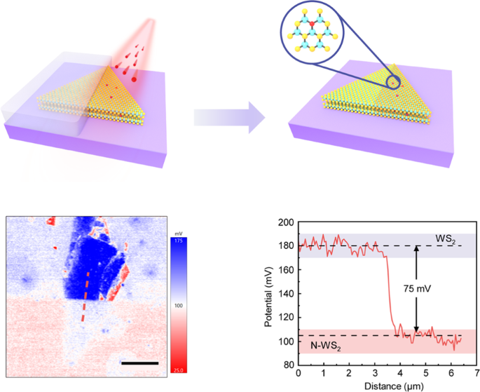
provides an effective way to directly modulate the performance of 2D MDs by low-energy ion implantation. RESULTS Figure 1 illustrates the fabrication process of the lateral WS2 p-n
homojunction realized by low-energy N-ion implantation. Initially, the WS2 flakes were mechanically exfoliated onto the Si/SiO2 substrates. Subsequently, a mask was created by spin-coating
Methyl methacrylate (MMA) and poly (methyl methacrylate) (PMMA) on top of the flakes. Then, electron beam lithography (EBL) and development were carried out to reveal the selected region of
the flake, while the remaining region was covered by MMA/PMMA. Whereafter, the low-energy nitrogen ions were successfully implanted into the uncovered WS2 flake. To calculate the stopping
range of nitrogen ions in the WS2 flake, SRIM Monte Carlo simulations were performed. It was worth noting that the implantation energy was 300 eV (with a projected range of 1.8 nm), which
ensured that the nitrogen dopants could remain in the lattice of WS2 flake (Fig. S1). After acetone treatment, the seamless lateral WS2 p-n homojunction was obtained. The optical microscope
(OM) image (Fig. 2a) indicates that the doped region maintains good morphology without visible damage. Raman spectra are carried out to further study the influence of the low-energy N-ion
implantation on the lattice structure. As plotted in Fig. 2b, it is observed that the Raman characteristic peak positions of pristine WS2 locate at 350.7 cm−1 (the in-plane vibrational
phonon mode of E12g) and 419.7 cm−1 (the out-of-plane vibrational phonon mode of A1g), consistent with previous reports32. Whereas, the E12g peak of N-WS2 (WS2 flake treated with low-energy
N-ion implantation) shows a slight blue shift about one wavenumber compared to the pristine sample. It is inferred that the doped nitrogen atom substitutes the position of sulfur atom and
forms a shorter W-N bond (W-N bond is 0.2018 nm, W-S bond is 0.2416 nm)11,13,33,34. This may be considered to introduce the compressive strain in the crystal lattice35. The slightly
decreased peak intensity indicates that the crystallization quality decreases slightly after the N-ion implantation process. Moreover, two small and sharp peaks have appeared at 148 cm−1
(Fig. S2a) and 384 cm−1 (Fig. S2b) after N-ion implantation treatment, which have been denoted as ZA(M) and A2’(M) phonon modes36. This result can be ascribed to the resonance Raman effect
caused by external substitution doping32,37,38, which indicates a successful nitrogen doping. After the rapid thermal annealing process, both the E12g peaks of N-WS2 and the pristine display
enhancement (Fig. S3). One of the possible reasons is that the rapid thermal annealing promotes the repairment of the lattice damage, and it improves the crystallization quality of the
implanted sample. Subsequently, the photoluminescence (PL) spectra of the materials are also investigated before and after the N-ion implantation process. As shown in Fig. 2c, the PL peak
energy position of pristine WS2 is located at ~1.93 eV, while N-WS2 shows the blue shift to ~1.96 eV. We utilize Lorenz peak decomposition to analyze the reasons. The upper part of Fig. 2c
shows that the PL peak of pristine WS2 is composed of two excitonic emission peak: the negative trions (X−) (lower energy) results from unintentional electrons doping provided by sulfur
vacancy and the neutral excitons (X0) (higher energy) originates from the intrinsic carrier recombination39,40. The PL peak of pristine WS2 is dominated by X− excitonic emission due to
unintentional electron doping provided by the sulfur vacancy defects39. In N-WS2, the doped nitrogen act as acceptors to introduce a large number of holes and deplete the residual electrons
to prevent the formation of X−. Thus, the PL peak of N-WS2 is dominated by switching to X0 recombination7, resulting in the peak blue shift as shown in the bottom part of Fig. 2c. Ion
implantation is a lossy doping approach, which can degrade the crystallization quality and induce some defects to trap carriers to form nonradiative recombination centers resulting in the
sharp decrease of PL intensity36. With the increase of N-ions implantation dose, the PL intensity continues to decrease, and eventually quenches (Fig. S4). After annealing treatment, the PL
intensities (Fig. S5) of both two samples are slightly enhanced, which can be explained by the following reasons: (1) removal of the residual organic matter and absorbents on the surface;
(2) repair of the damage lattice; (3) partial repair of the non-radiative recombination centers induced by ion bombardment. Atomic force microscopy (AFM) is utilized to measure the surface
morphology and the thickness of the as-fabricated lateral WS2 p-n homojunction. In Fig. 2d, the AFM image reveals the flat surface throughout the domain. Meanwhile, the sample thickness of
the N-implanted region is measured to be ~5 nm (~7 layers), which is about the same as the unimplanted region, indicating that the low-energy N-ions implantation does not reduce the
thickness of the WS2 flakes. This result excludes that the obtained p-type WS2 is caused by material thickness change and verifies that the N-ions implantation is the cause of the obtained
p-type WS241. Kelvin probe force microscopy (KPFM) is also implemented to investigate the potential change of WS2 flake before and after the N-ions implantation (Note S1). The contrastive
KPFM mapping is shown in Fig. 2e, the clear surface potential difference can be observed between the pristine WS2 and the N-WS2. Compare to pristine WS2, there is a significant decrease by
75 mV in surface potential for N-WS2 (Fig. 2f), corresponding to the increase in its work function. This further substantiates the p-type doping effect induced by N-ions implantation. In
order to intuitively characterize the presence and distribution of doped nitrogen element, the N-WS2 is characterized by high-angle annular dark-field (HAADF) scanning transmission electron
microscopy (STEM). In HAADF-STEM image, the brightness of atoms can be reflected by atomic number due to the Z-contrast, and atoms with higher atomic number produce brighter signal
intensity42. Substitution of S by N is predicted to produce darker contrasts. As depicted in Fig. 3a, the hexagonal honeycomb structure of N-WS2 is clearly visible, and the darker point at
the S site (the fourth atom in Line 1 and the sixth atom in Line 2) identified a N atom substituted to S site. The results are consistent with the theoretical calculation. Also, the line
profile intensity along the direction indicated by Line 1 and Line 2 agrees well with the HAADF-STEM image (Fig. 3b: top, Line 1; bottom, Line 2), further confirming the substitution of S by
N. As displayed in the energy dispersive spectroscope (EDS) elements mapping (Fig. 3c), W, S, and N elements are evenly distributed throughout the sample. Direct counting the number of N
atoms substituted gives doping concentration of 2.26% at the dose of 1 × 10¹⁵ ions cm−2 (Fig. S6). To further explore the influence of low-energy N-ion implantation on the electrical
properties of WS2, field-effect transistors (FETs) devices are fabricated. As illustrated in Fig. 4a, the sample is divided into three parts denoted as channel 1-2 (N-WS2), channel 2-3
(lateral WS2 p-n homojunction), and channel 3-4 (pristine WS2). The p-n junction is formed by a part of the implanted region and a part of the unimplanted region. Details of the device
fabrication process are given in the “Materials and methods” section. Noteworthy, to lower the Schottky barrier height, Au electrodes with a higher work function (~5.1 eV) contact are used
for N-WS2 contact, and Cr/Au electrodes with a lower work function (~4.6 eV) contact are used for WS2 contact. As shown in Fig. 4b, c, the output characteristic curves of both N-WS2 and
pristine WS2 at different gate voltages exhibit linear curves. It can be ascribed to ohmic contact between the appropriately selected metal electrodes and material. The output characteristic
curve of lateral WS2 p-n homojunction displayed in Fig. 4d presents that the junction has a significant rectification characteristic. The rectification ratio is approximately 550 under the
bias of ±2 V and the gate voltage of 60 V. To evaluate the property of the p-n homojunction, the ideality factor (_n_) is calculated by Shockley diode equation (Note S2). The ideality factor
of the p-n homojunction is about 1.46 at gate voltage of 60 V. This manifest that the current of the device is mainly dominated by the diffusion process rather than the recombination
process under the forward bias10. It is an indication of the relatively high quality of the junction. Figure 4e plots the transfer characteristic curves of pristine WS2 (blue curve) and
N-WS2 (red curve) with the implantation dose of 1 × 10¹⁴ ions cm−2. The pristine WS2 exhibits typical n-type conduction due to the sulfur vacancies contributing more electrons39. As well as
the current on/off ratio reaches 108. Conversely, N-WS2 FET shows a remarkable p-type conduction, which is undoubtedly caused by the N-ion implantation. This is because the N-ion
implantation injects a large number of holes, which causes the hole concentration to be much higher than the electron concentration, making the holes become the majority carriers in N-WS2.
We calculated the carrier concentration to be 1.49 × 1012 cm−2 for electron concentration and 4.09 × 1012 cm−2 for hole concentration at zero gate voltage (Note S3). However, the carrier
mobility and the current on/off ratio of N-WS2 are rather low just after implantation (Fig. S7). Actually, rapid thermal annealing is an effective way to activate the implanted ions, which
leads to the obvious improvement of the carrier mobility. We obtained that the hole mobility is increased to 12.16 cm2 V−1 s−1 (Note S4), and the current on/off ratio is also raised to 3.9 ×
106 compared to the unannealed FET. Table 1 summarizes the electrical performance parameters obtained from other 2D MDs and doping techniques. The N-WS2 FET in this work is equal or
superior to the devices acquired by other doping means. The improved performance of N-WS2 FET after rapid thermal annealing can be understood by the following, during the implantation
process, energetic N-ions will generate a series of elastic collision in WS2, and transfer energy to the atoms of WS2 indiscriminatingly. The colliding atoms will be released from the
original lattice sites when they gain enough energy. It’s worth noting that the atomic mass of the sulfur atom is less than that of the tungsten atom, and thus it is easier for sulfur atoms
to be unbound during the implantation process. Consequently, N-ions implantation will cause a series of damages in the form of substitutions, interstitials and vacancies in the implanted
WS243,44. The carrier mobility and conductivity will decrease significantly. However, the rapid thermal annealing process can activate the implanted nitrogen to migrate to the substitutional
sites and repair the crystal lattice damage of the material caused by the ion implantation process. As a result, the carrier mobility and conductivity of the sample are significantly
improved compared to the unannealed samples. In addition, annealing can remove the organic matter adsorbed on the surface of the channel materials to improve the interface quality and
reducing the carrier scattering. Moreover, it may improve the contact between electrodes and semiconductors, leading to the lowering of contact resistance, which is also benefit to the
improvement of device performance30. In order to investigate the influence of N-ions implantation doses on WS2 p-type doping level, the FETs devices are prepared with different implantation
doses. Figures 4e and S8 show the transfer characteristic curves of WS2 FET (blue line) and N-WS2 FET (red line) at gradient doses respectively. The electrical properties are recorded after
annealing. All pristine WS2 FETs exhibit typical n-type conduction. As the implantation dose increases, the p-type doping level becomes more significant. At the rather low dose of 1 × 10¹²
ions cm−2, the N-WS2 FET still shows electron-dominant n-type conduction. But the threshold voltage is shifted to the right compared to the pristine WS2 FET, indicating the weak p-type
doping caused by the N-ions implantation doses. When the dose is increased to 1 × 10¹³ ions cm−2, the current corresponding to the negative gate voltage starts to increase and the current
corresponding to the positive gate voltage decreases. This means that N-ions implantation can effectively improve the hole concentration and change the conductivity type from
electron-dominant n-type to bipolar-type. When the dose is further increased to 1 × 10¹⁴ ions cm−2, the hole concentration is much higher than the electron concentration. Therefore, the
conduction polarity of the N-WS2 FET completely changes to the hole-dominant p-type conduction. At the higher dose of 1 × 10¹⁵ ions cm−2, the off-state characteristic of N-WS2 FETs cannot be
well regulated by the gate voltage. To sum up, we successfully realize the regulation of the conductivity type of WS2 by precisely changing the N-ion implantation doses. The implanted WS2
can sequentially transform the conductivity type from n-type to bipolar- or even p-type conduction. In order to assess the device uniformity of p-type doped WS2, we calculate the hole
concentration and mobility of N-WS2 on the same device for ten cycles, as depicted in Fig. S9. The cycling performance of N-WS2 exhibits remarkable stability and remains unaffected by an
increase in cycle numbers. Additionally, we calculate the hole concentration and mobility of N-WS2 across different devices, as illustrated in Fig. S10, the performance of different devices
shows little difference. Subsequently, we verify the device stability of N-ion doping. After 3 months of vacuum preservation, the N-WS2 FET performance is slightly degraded and still
exhibits p-type characteristic (Fig. S11). This means that low-energy ion implantation is a stable doping method for 2D materials. To further understand our experimental result, density
functional theory (DFT) is employed to explore the doping effect and electronic structure of N-WS2. We construct four hypothetically possible models of N-doped sites (Fig. S12), including
substitutions (NS and NW) and interstitials (Abs-W and Abs-S), and calculate their formation energy. More detailed modeling parameters are provided in “Materials and methods” section. As
shown in the DFT calculations results, the substitution of N atom at S site (NS) has the lowest formation energy among the four possible doping models (Fig. 5a). The theoretical model of NS
matches the experimental observation results of HADDF-STEM (Fig. 3). The theoretical calculation results prove once again that the implanted N-ions primarily exist as substitution sites for
S atoms in a few-layer WS2. Therefore, in the subsequent calculation of the electronic structure of N-WS2, we only consider the condition of NS. To reveal the reason for p-type doping, we
have conducted calculations for the total density of states (TDOS) and partial density of the states (PDOS), as depicted in Figs. 5b and S13. According to the TDOS, after aligning the vacuum
levels, it is clear that the Fermi level shifts toward the valence band maximum (VBM) after N-ions implantation. We also calculate the work functions of pristine WS2 and N-WS2. As shown in
Fig. S14, the work function of WS2 exhibits an increase after N doping, which is consistent with the observed trend in KPFM measurements (Fig. 2e, f). The potential profiles obtained from
KPFM demonstrate a significant decrease in surface potential for WS2 after N doping, corresponding to the observed increase in its work function. This further substantiates the p-type doping
effect. As depicted in PDOS calculation (Fig. S13), the electronic states near the Fermi energy level of pristine WS2 are mainly caused by the hybridization between the W 5d orbitals and
the S 3p orbitals. After N-ions implanted into the WS2 crystal, the impurity states emerge in close proximity to the Fermi level, resulting in shallow acceptor levels above the VBM in WS2.
Notably, these impurity states predominantly originate from N 2p orbital contributions. All evidences prove that N doping can induce a p-type doping effect on WS2. Finally, to verify the
universality of the method to regulate the conductivity type of MDs via low-energy N-ion implantation, we extend this method to other 2D MD semiconductors. Figures 4f and S15 plot the
transfer characteristic curves of pristine and N-doped FETs on WSe2, SnS2, and MoS2, respectively. Their conductivity types are significantly transformed from n-type to p-type conduction
after low-energy N-ion implantation. In recent years, photodetectors without external power supply have attracted great attention. Because they can reduce energy consumption. It has great
application prospects in optical communication, infrared detection and so on45. The p-n junction is the best candidate. Because it has a natural built-in electric field, which can promote
the separation of electron-hole pairs and enhance the optical properties of 2D MDs materials. Based on this, we fabricate a photodetector based on the lateral WS2 p-n homojunction. Figure 6a
shows the schematic illustration of the photodetector based on lateral WS2 p-n homojunction. The detailed device fabrication process is described in the “Materials and methods” section.
Figure 6b shows the output characteristic curves before and after 532 nm laser illumination, the low dark current is 14.57 pA at 3 V bias without gate voltage. Under laser illumination, the
current increases obviously and rises with the increase of light power density. Increasing the light power density can increase the number of photogenerated carriers, resulting in higher
photocurrents46. The photodetector shows apparent photovoltaic effects under the 532 nm laser of 1.7 mW cm−2 with an open circuit voltage of 0.39 V and a short circuit current of −18.88 pA
(Fig. 6c). Figure 6d illustrates the energy band diagram of lateral WS2 p-n homojunction under illumination which can explain the change of the photo-response. As can be seen from the
surface potential measured by KPFM (Fig. 2e, f), there exists a built-in electric field pointed from WS2 to N-WS2 at the depletion region to prevent the infinite diffusion of the intrinsic
carrier. When the device exposed to light, the photogenerated carriers will be separated by the built-in electric field. The photogenerated electrons drift to the WS2 region while the
photogenerated holes drift to the N-WS2 region, generating a photocurrent. As shown in Fig. 6e, f, the response speed of the photodetector is expressed by the rise time and fall time, which
calculated as the time difference value between 10% (90%) and 90% (10%) of the high level47. It can be deduced that the rise and fall times are 5.6 ms and 4 ms at bias of 1 V. The transient
photo-response is studied under the periodic laser pulse of 2 s. Figure 6g depicts optical switching behavior of the photodetector measured at zero gate voltage and zero bias. When the laser
is turned on, the current rises rapidly and remains stable, then falls rapidly when the laser is turned off. The on-off state can switch rapidly and the current can still remain stable
after several cycles indicating that the high light current is contributed by the photogenerated carriers rather than the heating effect caused by laser48. Under varying light power
densities, the photo-response current raises as the light power density increases. To investigate the capability of the photodetector to detect different wavelength lasers, three different
wavelength lasers of 445 nm, 532 nm, and 638 nm were employed. Figure 6h plots the output characteristic curve of the three laser sources mentioned above at the light power density of 4.1 mW
cm−2. The longer the incident wavelength, the higher the current generated. As the wavelength of laser light increases, the energy of photons decreases due to their inverse relationship.
Consequently, when maintaining a constant light power density over a given time period, an increase in photon generation occurs as a result of lower photon energy, leading to an amplified
photocurrent49. As depicted in Fig. S16, the transient photo-response diagram of different wavelength lasers (4.1 mW cm−2) shows that the photodetector exhibits stable switching behavior
under different wavelength lasers illumination. The parameters used to evaluate the performance of the photodetector are mainly responsivity (_R_), detectivity (_D__*_) and external quantum
efficiency (_EQE_). _R_ is described as the ability of the photon to generate electron-hole pairs. It is calculated as \(R(A{{W}}^{-1})=\frac{{I}_{{ph}}}{\rho S}\), where \({I}_{{ph}}\),
\(\rho\) and _S_ are expressed as photogenerated current, light power density and effective illumination area, respectively47. Moreover, _D__*_ is defined as the ability to detect weak
light, i.e., \({D}^{* }\left({Jones}\right)=\,\frac{R\sqrt{S}}{\sqrt{2e{I}_{{dark}}}}\), where _e_, _R_ and \({I}_{{dark}}\) are the electron charge, the responsivity and the dark current47.
The _EQE_ is expressed as the ratio of the number of electrons generated by the incident photon to the number of the incident photons per unit time. It is given by the equation,
\({EQE}\left( \% \right)=\frac{{Rhc}}{\lambda e}\times 100 \%\), where _R_, _h_, _c_, \(\lambda\) and _e_ are the responsivity, Planck’s constant, light speed, incident wavelength and
electron charge, respectively47. Figures 6i and S17 display the light power density dependence relation of _R_, _D__*_, and _EQE_. With the increase of the light power density from 1.7 mW
cm−2 to 6.38 mW cm−2, _R_, _D__*_, and _EQE_ show a decreasing trend. This result is related to the increasing recombination probability of photocarriers at increasing light power density50.
Under the zero bias, the maximum _R_, _D__*_, and _EQE_ values reach to 35 mA W−1, 9.8 × 10¹⁰ Jones and 8.17%, respectively (532 nm laser of 1.7 mW cm−2). In addition, the _R_, _D__*_, and
_EQE_ curves of the photodetector at different laser wavelengths are shown in Fig. S18. It can be discovered that the value of _R_, _D__*_, and _EQE_ reach the highest under the 532 nm
laser. Thereby, the main performance of the photodetector is measured under the 532 nm laser. DISCUSSION In conclusion, we have demonstrated a strategy for selective p-type doping via
low-energy N-ion implantation. Low-energy N-ions of 300 eV have been implanted into few-layer WS2 flakes, which ensure the nitrogen dopants remain in the lattice of WS2 flake. By accurately
controlling the N-ions implantation doses, we successfully control the transformation of the n-type semiconductor WS2 into the bipolar- or even the p-type semiconductor. After rapid thermal
annealing, the current on/off ratio and hole mobility of N-doped WS2 greatly enhanced. Moreover, this strategy is also applicable to several other MDs semiconductors including WSe2, SnS2,
and MoS2. Based on the lateral WS2 p-n homojunction, the photodetector has been obtained. In this work, a purely physical method of low-energy ion implantation is proposed to realize
selective p-type doping on MDs. By replacing the high-energy ion source with a lower-energy source, the performance of 2D materials can be directly and accurately modulated. MATERIALS AND
METHODS SAMPLES PREPARATION High-quality few-layer WS2, WSe2, SnS2, and MoS2 flakes were mechanically exfoliated from their bulk crystal (Shanghai Onway Technology Co., Ltd.) and transferred
onto 300 nm SiO2/Si substrates. Methyl methacrylate (MMA) and polymethyl methacrylate (PMMA) were spin-coated at 600 rpm for 6 s and 4000 rpm for 60 s to cover the flakes, and then baked at
120 °C for 1 min and 5 min, respectively. Electron beam lithography (EBL) and the following development were carried out to expose the selected region of the flakes, while the remaining
region was covered by MMA/PMMA. Subsequently, the low-energy ions implantation technology was employed to implant N-ions into the selected region of WS2 flakes. After acetone treatment, a
seamless lateral WS2 p-n homojunction was obtained. LOW-ENERGY ION IMPLANTATION PROCESS A low-energy ion implantation system with an adjustable ion energy of 300 eV–1.5 keV was used to
implant nitrogen ions into 2D materials. When the vacuum was pumped below 6 × 10⁻⁴ Pa, nitrogen gas was introduced into the vacuum chamber, and stabilized the pressure in the chamber at 1.2
× 10−2 Pa. Subsequently, the nitrogen ions were extracted after ionization and screening processes, then the nitrogen ions were then implanted into the 2D material within a vacuum chamber
using an accelerating voltage of 300 V. DEVICE FABRICATION The FET devices were fabricated by EBL and thermal evaporation. MMA and PMMA were spin-coated to cover the lateral WS2 p-n
homojunction, using the same parameters as mentioned above. EBL was used to prepare the electrode patterns, including the regions of WS2, N-WS2, and lateral p-n homojunction on the same
sample. The thermal evaporation was used for depositing the metal contact electrodes with 15 nm Cr and 50 nm Au for WS2 (electrode 3 and 4 in Fig. 4a) and 65 nm Au for N-WS2 (electrode 1 and
2 in Fig. 4a). After the device were prepared, rapid thermal annealing at 400 °C for 5 min was performed to improve the device performance. DENSITY FUNCTIONAL THEORY CALCULATION Density
functional theory (DFT) calculations were performed by using CASTEP code package. The electronic exchange-correlation potential was carried out using the Perdew–Burke–Ernzerhof (PBE)
functional of the generalized gradient approximation (GGA) and the ultrasoft pseudopotentials. The Brillouin zone integration was sampled and calculated by using a 1 × 2 × 1 Monkhorst-Pack
k-point mesh. The kinetic energy cut-off was set as 500 eV for the plane-wave basis set. Van der Waals interactions were taken into account using the DFT dispersion (DFT-D) correction. To
optimize the geometry, the convergence tolerances were set to be 5 × 10⁻⁶ eV energy per atom, 5 × 10⁻⁴ Å maximum displacement, and 0.01 eV Å−1 maximum force. A four-layer WS2 (100) plane
supercell (W32S64) was first constructed with a vacuum region of 15 Å along the z-axis for calculation. Additionally, considering that we mainly used ion implantation to modify the surface
of WS2, the WS2 with two layers on the upper surface was considered to achieve N substitution doping and surface adsorption. DEVICE CHARACTERIZATION MORPHOLOGY AND COMPOSITION
CHARACTERIZATION The optical microscopy images were obtained by an optical microscope (OLYMPUS BX51). Raman and PL spectra were characterized by the confocal Raman and Photoluminescence
spectroscopy (LabRAM HR Evolution of HORIBA) with a 532 nm laser at room temperature. Atomic force microscopy (Jupiter XR) was used to measure the thickness of the materials. Kelvin probe
force microscopy (Jupiter XR) was used to measure the surface potential of lateral p-n junction. High-angle annular dark-field (HAADF) scanning transmission electron microscopy (STEM) image
and energy-dispersive spectrometer (EDS) mapping were carried out by JEM-ARM200CF. The measurements of electrical and optical properties were measured by the semiconductor device parameter
analyzer instrument (TOSTAR 5514B) and vacuum probe station (Lake Shore, TTPX). The properties of the photodetector were measured under 445 nm, 532 nm, and 638 nm laser. REFERENCES * Liu,
Y., Huang, Y. & Duan, X. F. Van der Waals integration before and beyond two-dimensional materials. _Nature_ 567, 323–333 (2019). Article ADS Google Scholar * Pei, Y. F. et al. Recent
progress about 2D metal dichalcogenides: synthesis and application in photodetectors. _Nano Res._ 14, 1819–1839 (2021). Article Google Scholar * Liu, Y. et al. Promises and prospects of
two-dimensional transistors. _Nature_ 591, 43–53 (2021). Article ADS Google Scholar * Liu, C. Y. et al. Silicon/2D-material photodetectors: from near-infrared to mid-infrared. _Light Sci.
Appl._ 10, 123 (2021). Article ADS Google Scholar * Lee, D. et al. Remote modulation doping in van der Waals heterostructure transistors. _Nat. Electron._ 4, 664–670 (2021). Article
Google Scholar * Wang, H. Y. et al. Junction field‐effect transistors based on PdSe2/MoS2 heterostructures for photodetectors showing high responsivity and detectivity. _Adv. Funct. Mater._
31, 2106105 (2021). Article Google Scholar * Wang, Z. Y. et al. Substitutional p-type doping in NbS2-MoS2 lateral heterostructures grown by MOCVD. _Adv. Mater._ 35, 2209371 (2023).
Article Google Scholar * Wu, W. H. et al. Self-powered photovoltaic photodetector established on lateral monolayer MoS2-WS2 heterostructures. _Nano Energy_ 51, 45–53 (2018). Article
Google Scholar * Li, Z. X. et al. Universal p-type doping via lewis acid for 2D transition-metal dichalcogenides. _ACS Nano_ 16, 4884–4891 (2022). Article Google Scholar * Sun, J. C. et
al. Lateral 2D WSe2 p-n homojunction formed by efficient charge-carrier-type modulation for high-performance optoelectronics. _Adv. Mater._ 32, 1906499 (2020). Article Google Scholar *
Tang, B. S. et al. Direct n- to p-type channel conversion in monolayer/few-layer WS2 field-effect transistors by atomic nitrogen treatment. _ACS Nano_ 12, 2506–2513 (2018). Article Google
Scholar * Mitta, S. B. et al. Gate-modulated ultrasensitive visible and near-infrared photodetection of oxygen plasma-treated WSe2 lateral pn-homojunctions. _ACS Appl. Mater. Interfaces_
12, 23261–23271 (2020). Article Google Scholar * Qian, Q. K. et al. Photoluminescence induced by substitutional nitrogen in single-layer tungsten disulfide. _ACS Nano_ 16, 7428–7437
(2022). Article Google Scholar * Li, W. Q. et al. A review of recent applications of ion beam techniques on nanomaterial surface modification: design of nanostructures and energy
harvesting. _Small_ 15, 1901820 (2019). Article Google Scholar * Li, Z. Q. & Chen, F. Ion beam modification of two-dimensional materials: characterization, properties, and
applications. _Appl. Phys. Rev._ 4, 011103 (2017). Article ADS Google Scholar * Pelgrin, V., Yoon, H., Cassan, E. & Sun, Z. et al. Hybrid integration of 2D materials for on-chip
nonlinear photonics. _Light.: Adv. Manuf._ 4, 28 (2023). Google Scholar * Qu, Y. et al. Integrated optical parametric amplifiers in silicon nitride waveguides incorporated with 2D graphene
oxide films. _Light.: Adv. Manuf._ 4, 35 (2023). Google Scholar * Lee, D. et al. Hyperbolic metamaterials: fusing artificial structures to natural 2D materials. _eLight_ 2, 1 (2022).
Article Google Scholar * Guo, Z. et al. In-situ neutron-transmutation for substitutional doping in 2D layered indium selenide based phototransistor. _eLight_ 2, 9 (2022). Article Google
Scholar * Liu, Y. R. et al. Defect engineering of out-of-plane charge transport in van der Waals heterostructures for Bi-direction photoresponse. _ACS Nano_ 15, 16572–16580 (2021). Article
Google Scholar * Thiruraman, J. P., Masih Das, P. & Drndić, M. Irradiation of transition metal dichalcogenides using a focused ion beam: controlled single-atom defect creation. _Adv.
Funct. Mater._ 29, 1904668 (2019). Article Google Scholar * Wang, G. et al. Seamless lateral graphene p-n junctions formed by selective in situ doping for high-performance photodetectors.
_Nat. Commun._ 9, 5168 (2018). Article ADS Google Scholar * Chen, R. et al. A high‐speed photodetector fabricated with tungsten‐doped MoS2 by ion implantation. _Adv. Electron. Mater._ 8,
2200281 (2022). Article Google Scholar * Kretschmer, S. et al. Threshold ion energies for creating defects in 2D materials from first-principles calculations: chemical interactions are
important. _J. Phys. Chem. Lett._ 13, 514–519 (2022). Article Google Scholar * Willke, P. et al. Doping of graphene by low-energy ion beam implantation: structural, electronic, and
transport properties. _Nano Lett._ 15, 5110–5115 (2015). Article ADS Google Scholar * He, S. M. et al. Spectroscopic and electrical characterizations of low-damage phosphorous-doped
graphene via ion implantation. _ACS Appl. Mater. Interfaces_ 11, 47289–47298 (2019). Article Google Scholar * Murray, R. et al. The effect of low energy ion implantation on MoS2. _ECS J.
Solid State Sci. Technol._ 5, Q3050–Q3053 (2016). Article Google Scholar * Bangert, U. et al. Ion-beam modification of 2-D materials - single implant atom analysis via annular dark-field
electron microscopy. _Ultramicroscopy_ 176, 31–36 (2017). Article Google Scholar * Bui, M. N. et al. Low-energy Se ion implantation in MoS2 monolayers. _npj 2D Mater. Appl._ 6, 42 (2022).
Article Google Scholar * Prucnal, S. et al. Chlorine doping of MoSe2 flakes by ion implantation. _Nanoscale_ 13, 5834–5846 (2021). Article Google Scholar * Bertolazzi, S. et al.
Engineering chemically active defects in monolayer MoS2 transistors via ion-beam irradiation and their healing via vapor deposition of alkanethiols. _Adv. Mater._ 29, 1606760 (2017). Article
Google Scholar * Cong, C. X. et al. Synthesis and optical properties of large-area single-crystalline 2D semiconductor WS2 monolayer from chemical vapor deposition. _Adv. Opt. Mater._ 2,
131–136 (2014). Article Google Scholar * Zhao, X. et al. Effective p-type N-doped WS2 monolayer. _J. Alloy. Compd_ 649, 357–361 (2015). Article Google Scholar * Cao, Q. et al. Realizing
stable p-type transporting in two-dimensional WS2 films. _ACS Appl. Mater. Interfaces_ 9, 18215–18221 (2017). Article Google Scholar * Azcatl, A. et al. Covalent nitrogen doping and
compressive strain in MoS2 by remote N2 plasma exposure. _Nano Lett._ 16, 5437–5443 (2016). Article ADS Google Scholar * Shi, W. et al. Raman and photoluminescence spectra of
two-dimensional nanocrystallites of monolayer WS2 and WSe2. _2D Materials_ 3, 025016 (2016). Article Google Scholar * Chang, R. J. et al. Postgrowth substitutional tin doping of 2D WS2
crystals using chemical vapor deposition. _ACS Appl. Mater. Interfaces_ 11, 24279–24288 (2019). Article Google Scholar * Sasaki, S. et al. Growth and optical properties of Nb-doped WS2
monolayers. _Appl. Phys. Express_ 9, 071201 (2016). Article ADS Google Scholar * Carozo, V. et al. Optical identification of sulfur vacancies: bound excitons at the edges of monolayer
tungsten disulfide. _Sci. Adv._ 3, e1602813 (2017). Article ADS Google Scholar * Wang, Y. L. et al. Strain-induced direct–indirect bandgap transition and phonon modulation in monolayer
WS2. _Nano Res._ 8, 2562–2572 (2015). Article Google Scholar * Xia, H. et al. Pristine PN junction toward atomic layer devices. _Light Sci. Appl._ 11, 170 (2022). Article ADS Google
Scholar * Murai, Y. et al. Versatile post-doping toward two-dimensional semiconductors. _ACS Nano_ 15, 19225–19232 (2021). Article Google Scholar * Ronning, C. Ion implantation into
gallium nitride. _Phys. Rep._ 351, 349–385 (2001). Article ADS Google Scholar * Ronning, C. et al. Ion beam doping of semiconductor nanowires. _Mater. Sci. Eng.: R: Rep._ 70, 30–43
(2010). Article Google Scholar * Qiao, H. et al. Self‐powered photodetectors based on 2D materials. _Adv. Opt. Mater._ 8, 1900765 (2020). Article Google Scholar * Lin, X. et al.
High-performance photodetector and its optoelectronic mechanism of MoS2/WS2 vertical heterostructure. _Appl. Surf. Sci._ 546, 149074 (2021). Article Google Scholar * Long, M. S. et al.
Progress, challenges, and opportunities for 2D material based photodetectors. _Adv. Funct. Mater._ 29, 1803807 (2019). Article Google Scholar * Yang, H. et al. Bolometric effect in Bi2O2Se
photodetectors. _Small_ 15, 1904482 (2019). Article Google Scholar * Li, C. H. et al. The photodetectors based on lateral monolayer MoS2/WS2 heterojunctions. _Nanoscale Res. Lett._ 16,
123 (2021). Article ADS Google Scholar * Wu, D. et al. Ultrabroadband and high-detectivity photodetector based on WS2/Ge heterojunction through defect engineering and interface
passivation. _ACS Nano_ 15, 10119–10129 (2021). Article Google Scholar * Zhang, Y. W. et al. An ultrafast WSe2 photodiode based on a lateral _p-i-n_ homojunction. _ACS Nano_ 15, 4405–4415
(2021). Article Google Scholar * Tao, R. et al. Tune the electronic structure of MoS2 homojunction for broadband photodetection. _J. Mater. Sci. Technol._ 119, 61–68 (2022). Article
Google Scholar * Kozhakhmetov, A. et al. Controllable p-type doping of 2D WSe2 via vanadium substitution. _Adv. Funct. Mater._ 31, 2105252 (2021). Article Google Scholar * Vu, V. T. et
al. Synthesis of a selectively Nb-doped WS2–MoS2 lateral heterostructure for a high-detectivity PN photodiode. _ACS Nano_ 16, 12073–12082 (2022). Article Google Scholar Download references
ACKNOWLEDGEMENTS This work was financially supported by the National Natural Science Foundation of China (12025503, U23B2072, 12074293, and 12275198), the Fundamental Research Funds for the
Center Universities (2042024kf0001 and 2042023kf0196). AUTHOR INFORMATION AUTHORS AND AFFILIATIONS * School of Physics and Technology, Key Lab of Artificial Micro- and Nano-Structures of
Ministry of Education, Wuhan University, Wuhan, China Yufan Kang, Yongfeng Pei, Dong He, Hang Xu, Mingjun Ma, Jialu Yan, Changzhong Jiang, Wenqing Li & Xiangheng Xiao Authors * Yufan
Kang View author publications You can also search for this author inPubMed Google Scholar * Yongfeng Pei View author publications You can also search for this author inPubMed Google Scholar
* Dong He View author publications You can also search for this author inPubMed Google Scholar * Hang Xu View author publications You can also search for this author inPubMed Google Scholar
* Mingjun Ma View author publications You can also search for this author inPubMed Google Scholar * Jialu Yan View author publications You can also search for this author inPubMed Google
Scholar * Changzhong Jiang View author publications You can also search for this author inPubMed Google Scholar * Wenqing Li View author publications You can also search for this author
inPubMed Google Scholar * Xiangheng Xiao View author publications You can also search for this author inPubMed Google Scholar CONTRIBUTIONS Y.F.K., C.Z.J., and X.H.X. conceived the project.
Y.F.K. designed and fabricated the devices, carried out the experiments and measurements. Y.F.P. assisted in fabricating the devices; Y.F.K., Y.F.P., and W.Q.L. analyzed the results and
prepared the manuscript; D.H. contributed to the simulation. H.X. and W.Q.L. drew the schematic diagram; X.H.X. supervised the project. All the other authors contributed to the manuscript.
CORRESPONDING AUTHORS Correspondence to Wenqing Li or Xiangheng Xiao. ETHICS DECLARATIONS CONFLICT OF INTEREST The authors declare no competing interests. SUPPLEMENTARY INFORMATION
SUPPLEMENTARY INFORMATION RIGHTS AND PERMISSIONS OPEN ACCESS This article is licensed under a Creative Commons Attribution 4.0 International License, which permits use, sharing, adaptation,
distribution and reproduction in any medium or format, as long as you give appropriate credit to the original author(s) and the source, provide a link to the Creative Commons licence, and
indicate if changes were made. The images or other third party material in this article are included in the article’s Creative Commons licence, unless indicated otherwise in a credit line to
the material. If material is not included in the article’s Creative Commons licence and your intended use is not permitted by statutory regulation or exceeds the permitted use, you will
need to obtain permission directly from the copyright holder. To view a copy of this licence, visit http://creativecommons.org/licenses/by/4.0/. Reprints and permissions ABOUT THIS ARTICLE
CITE THIS ARTICLE Kang, Y., Pei, Y., He, D. _et al._ Spatially selective p-type doping for constructing lateral WS2 p-n homojunction via low-energy nitrogen ion implantation. _Light Sci
Appl_ 13, 127 (2024). https://doi.org/10.1038/s41377-024-01477-3 Download citation * Received: 09 October 2023 * Revised: 13 April 2024 * Accepted: 10 May 2024 * Published: 30 May 2024 *
DOI: https://doi.org/10.1038/s41377-024-01477-3 SHARE THIS ARTICLE Anyone you share the following link with will be able to read this content: Get shareable link Sorry, a shareable link is
not currently available for this article. Copy to clipboard Provided by the Springer Nature SharedIt content-sharing initiative