- Select a language for the TTS:
- UK English Female
- UK English Male
- US English Female
- US English Male
- Australian Female
- Australian Male
- Language selected: (auto detect) - EN
Play all audios:
ABSTRACT Recently, integrated photonics has attracted considerable interest owing to its wide application in optical communication and quantum technologies. Among the numerous photonic
materials, lithium niobate film on insulator (LNOI) has become a promising photonic platform owing to its electro-optic and nonlinear optical properties along with ultralow-loss and
high-confinement nanophotonic lithium niobate waveguides fabricated by the complementary metal–oxide–semiconductor (CMOS)-compatible microstructure engineering of LNOI. Furthermore,
ferroelectric domain engineering in combination with nanophotonic waveguides on LNOI is gradually accelerating the development of integrated nonlinear photonics, which will play an important
role in quantum technologies because of its ability to be integrated with the generation, processing, and auxiliary detection of the quantum states of light. Herein, we review the recent
progress in CMOS-compatible microstructure engineering and domain engineering of LNOI for integrated lithium niobate photonics involving photonic modulation and nonlinear photonics. We
believe that the great progress in integrated photonics on LNOI will lead to a new generation of techniques. Thus, there remains an urgent need for efficient methods for the preparation of
LNOI that are suitable for large-scale and low-cost manufacturing of integrated photonic devices and systems. SIMILAR CONTENT BEING VIEWED BY OTHERS INTEGRATED ELECTRO-OPTICS ON THIN-FILM
LITHIUM NIOBATE Article 25 April 2025 HIGH DENSITY LITHIUM NIOBATE PHOTONIC INTEGRATED CIRCUITS Article Open access 10 August 2023 LITHIUM NIOBATE PHOTONIC-CRYSTAL ELECTRO-OPTIC MODULATOR
Article Open access 17 August 2020 INTRODUCTION In contemporary society, the demand for high-bandwidth optical communication, including for mobile high-definition video streaming, autonomous
vehicle applications, remote surgery, telepresence applications, and interactive 3D virtual reality gaming, is sharp increasing1,2,3,4,5. The electro-optical modulator is the key component
in optical fiber communication, which modulates the light signal for loading information through electricity. Lithium niobate (LiNbO3, LN) exhibits a high-performance electro-optic effect
and high optical transparency6,7. Therefore, LiNbO3 has been widely applied in electro-optic modulators. Generally, optical modulation is realized by a voltage-induced refractive index
change, which can be described by the change in the ellipsoid of the refraction index influenced by an external electric field as \(\Delta \beta _{ij} = \gamma _{ijk}E_k + h_{ijkl}E_kE_l +
\ldots\), where Δβ_ij_ is the variation in the dielectric impermeability under the external electric field (_E_), γ_ijk_ is the linear electro-optic coefficient or Pockels coefficient, and
_h__ijkl_ is the quadratic electro-optic coefficient or Kerr coefficient. For LN, the linear electro-optic coefficient is _γ_33 = 30.9 × 10⁻¹² mV−1, while other photonic materials usually
have a very small or zero linear electro-optic coefficient. For example, the linear electro-optic coefficient of GaAs is _γ_41 = 1.5 × 10⁻¹² mV−1, which is one-twentieth that of LN. An
electro-optic modulator can be constructed on LN wafers by fabricating waveguides via defect engineering, including titanium diffusion or proton exchange, which is compatible with
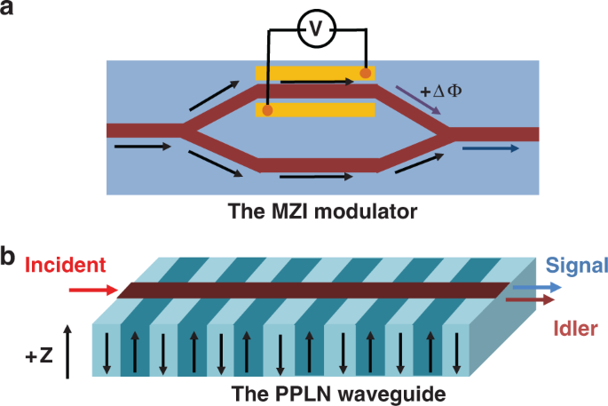
complementary metal–oxide–semiconductor (CMOS) technology. For example, the 50:50 Y-junction microstructure splits the input light into two LN optical waveguides that form the two arms of
the Mach–Zehnder interferometer (MZI) modulator, a traditional electric-optical modulator. As shown in Fig. 1a, the applied voltage induces a phase delay in one arm and a phase advance in
the other, which in turn changes the output intensity at the Y-combiner through interference7. The minimum voltage required to completely switch the output between on and off is defined as
the half-wave voltage (_V_π). However, the low refractive index contrast of the titanium diffusion (Δ_n_ ~0.01) or proton exchange (Δ_n_ ~0.1) waveguides resulted in weak confinement and a
large bending radius of the waveguides8. The weak optical confinement requires metal electrodes to be placed far from the optical waveguide, which in turn lowers the electro-optic
efficiency. Hence, either large voltages or long electrodes are required to sufficiently modulate traditional LN modulators (with a size of approximately several centimeters). Therefore, the
product of the half-wave voltage and electrode length, _V_π_L_, is a common figure of merit for electro-optic modulators. Nevertheless, the capacitance of the long electrodes limits the
bandwidth, which results in a trade-off between the driving voltage and bandwidth7. On the other hand, ferroelectric domain engineering of LN crystals has been extended from 1D to 2D and 3D,
which was comprehensively reviewed in reference9. Periodically poled lithium niobate (PPLN) has been widely applied in the fields of frequency conversion, nonlinear beam shaping10, and
quantum entanglement based on quasi-phase-matching (QPM) theory11,12,13,14,15. The second-order nonlinear optical coefficients (_d_33 and _d_31) of LN are 25.2 and 4.6 pm V−1 at 1064 nm,
respectively16. Because LN is only poled along the _z_-axis, PPLN is appropriate for polarizing light to parallel to the _z_-axis to exploit the largest nonlinear-optical coefficient _d_33.
As shown in Fig. 1b, a channel waveguide was fabricated on the surface of a PPLN wafer, which can confine the pump beam over the entire interaction length to greatly increase the conversion
efficiency. Moreover, considering the device size, reliability, cost, and energy consumption, photonic integrated circuit (PIC) technology has recently attracted significant interest in the
rise of the integrated photonics field17,18,19,20,21,22,23. Integrated photonics is concerned with the integration of all the key components connected by a waveguide in a single chip
(photonic platform) using a single material (monolithic integration) or multiple materials (hybrid integration). Most integrated photonic circuits have been built on four key platforms:
indium phosphide24,25, silicon-on-insulator (SOI)26,27,28, silicon nitride25,29, and LN30,31. Nevertheless, no photonic platform has yet produced an optimal overall photonics system
performance17. Generally, the selection of a material platform is based on the functionality of the optical components in the circuit, a low propagation loss, and industry-compatible
fabrication processes18. For example, the compatibility of silicon integrated circuit manufacturing is the main reason for the development of silicon photonics32. Moreover, the manufacturing
methods are suitable for the construction of SOI rib waveguides with a small cross-section of 1 μm2 with propagation losses as low as 0.1–0.5 dB cm−1 and a high index contrast between the
Si waveguide layers (_n_Si ~3.4) and SiO2 cladding layers (_n_SiO2 ~1.4), affording strong optical confinement and a small bending radius of 10 μm33. The low propagation loss and high index
contrast of photonics systems, which make SOI one of the most active photonic platforms, are important evaluation standards for photonic platforms34. However, the 3 dB electrical modulation
bandwidths of all-Si photonic devices have a theoretical limit of approximately 60 GHz35. To conclude, LN is a promising photonic matrix due to its advantageous electro-optical effect and
nonlinear optical properties. For example, on-chip generation and manipulation of entangled photons based on annealed proton exchanged waveguide circuits integrated on a z-cut PPLN crystal
was demonstrated36. Unfortunately, bulk LN waveguides have large footprints, and the fabrication technology is not compatible with CMOS technology. Above all, nanophotonic LN waveguides with
a larger refractive index contrast and a smaller optical mode size have emerged as a branch of integrated lithium niobate photonics37,38,39,40, although LN was perceived as a
difficult-to-etch material. Over the past 25 years, integrated lithium niobate photonics have relied almost exclusively on high-quality lithium niobate thin film on insulator (LNOI)
technology41 and advanced PIC technology for etching nanophotonic waveguides and microphotonic modulators. On the one hand, LNOI with a diameter of 3 in. can be fabricated by the smart cut
technique41. In this technique, a submicron single-crystalline LN film is first detached from a sacrificial wafer by crystal ion slicing and then bonded with a SiO2-deposited LN substrate or
Si substrate, forming LNOI (Fig. 2a). On the other hand, the CMOS-compatible microstructure engineering of LNOI for integrated photonic circuits, including nanophotonic waveguides and
advanced functional modulators, has advanced considerably. Briefly, the microstructure of integrated photonic circuits is transferred to LN thin films by a lithographically defined mask.
Then, the LN thin film is etched by Ar+ milling, forming thin slabs with a thickness of several hundred nanometers, which form ridge waveguides. Finally, a microscale-thick SiO2 cladding
layer is deposited on top of the etched LN thin film by plasma-enhanced chemical vapor deposition (PECVD) to form a sandwich structure (Fig. 2b). The refractive index contrast between the LN
core (_n_LN ~2.1) and SiO2 cladding (_n_SiO2 ~1.4) is approximately 0.7, which is much larger than that of traditional LN waveguides; thus, LNOI can serve as strongly guiding planar
waveguides even with a core layer of sub-micron thickness. Furthermore, domain engineering of LNOI was studied systematically for phase-matching nonlinear photonics. CMOS-compatible domain
engineering of LNOI is gradually accelerating the development of integrated nonlinear photonics, which will play an important role in integrated photonic quantum technology42. In addition,
considering the difficulty of etching LN, microstructure engineering using an easy-to-etch photonic material (e.g., SOI or silicon nitride) rib-loaded on LNOI is an attractive approach for
hybrid integration of integrated photonic circuits, which not only obviates the necessity of etching LN but also combines the scalability of silicon photonics with the excellent
electro-optic modulation of LN43. Lithium niobate, as a traditional multifunctional material, has stimulated a photonics revolution as silicon did for electronics. Herein, we review the
progress in microstructure and domain engineering of LNOI for integrated lithium niobate photonics, including photonic modulation and nonlinear photonics. Above all, ultra low-loss highly
confined LN nanophotonic waveguides are the most fundamental building block17. Furthermore, the optical modulation device is at the heart of integrated lithium niobate photonic systems, as
it encodes the RF signal. In Section “Microstructure engineering of LNOI for photonic modulation”, the progress in the microstructure engineering of LNOI for the preparation of ultra
low-loss highly confined nanophotonic waveguides and microphotonic modulators is described. Furthermore, we review the progress in on-chip nonlinear photonics involving highly confined
photonic microstructures and phase-matching techniques for LNOI in Section “Microstructure engineering of LNOI for nonlinear integrated photonics”. The focus is on the domain engineering of
LNOI for QPM nonlinear photonics. MICROSTRUCTURE ENGINEERING OF LNOI FOR PHOTONIC MODULATION Generally, the basic microstructure of integrated photonic circuits for photonic modulation
contains ridge waveguides and microphotonic structures, including micro rings, microdisks, and microracetracks. Whispering-gallery-mode (WGM) microresonators are the most compact micro
modulator with high confinement of light into small ring volumes, such as microrings, microdisks, and microracetracks44. Optical WGM microresonators have some exceptional properties, such as
a small mode volume, a high power density, and a high-quality factor _Q_ (_Q_ = _λ_/Δλ, where _λ_ is the wavelength at which resonance occurs and Δ_λ_ is the linewidth of the resonance
wavelength). The refractive index changes when an electric field is applied to LN microresonators based on the electro-optic effect, which modifies the effective optical path length of the
resonator. Thus, the resonance frequency of the microresonator shifts, thereby realizing electrical tuning. In the early stage, efforts to construct microstructures on LNOI for photonic
modulation were focused on low-loss nanophotonic waveguides and high-Q microresonators. Furthermore, MZI modulators integrated on LNOI platforms with advanced functionalities have been
reported. In this section, both complementary microstructure engineering approaches for photonic circuits, i.e., direct etching of LNOI (monolithic integration) and using other photonic
materials rib-loaded on LNOI (hybrid integration), are reviewed. MICROSTRUCTURE ENGINEERING BY DIRECT ETCHING OF LNOI Z-CUT LN FILMS FOR TM POLARIZATION Generally, the development of WGM
microresonators for integrated lithium niobate photonics is accompanied by the improvement of the LNOI preparation technique. In the early stage, z-cut LN films were generally selected
because of the limitations of lithographic techniques. Metal electrodes can be deposited between the substrate and the waveguide so that an electric field can be applied along the z-axis to
exploit the largest electro-optic coefficient, _r_33, of LN, with light polarization along the _z_-axis (the electric field direction is mainly perpendicular to the LN film, which is called
transverse magnetic (TM) polarization) (Fig. 3a). To the best of our knowledge, a slab waveguide on LNOI was prepared for the first time by crystal ion slicing and wafer bonding (called the
smart cut method) in 200445. The electro-optic coefficients and refractive index of the LN film were found to be comparable to those of the bulk LN crystal. Ridge waveguides on LNOI were
first fabricated by photolithography and Ar+ beam milling46. However, the waveguide loss was not measured accurately and was estimated to be largely owing to the rough sidewalls caused by
the etching process. It must be noted that the large mismatch in the thermal expansions of LN and SiO2/Si substrates can generate strong thermal stress during the bonding and layer transfer
processes. Park et al.47 introduced laser irradiation for the layer transfer process to promote localized layer exfoliation on an LN donor substrate and obtained a 6 mm2 LNOI sample with a
microdisk structure. Later, Guarino et al.48 introduced benzocyclobutene (BCB) as an adhesive layer between the metal electrode and LN film to reduce thermal stress and successfully prepared
a centimeter-sized LNOI sample49. More importantly, an electro-optically tuneable WGM microresonator was introduced for the time on an LNOI platform. The transmission spectrum was tuned by
the electro-optic effect, with a frequency tunability of 0.14 GHz V−1. However, BCB did not allow high-temperature annealing to repair the implantation-induced defects, which resulted in an
electro-optical activity that was approximately 50% that of the bulk LN crystal and a large propagation loss of approximately 17 dB cm−1. Nevertheless, the study validated the viability of
integrated lithium niobate photonics and stimulated further research on ultralow-loss sub-micron waveguides. Hu and co-workers prepared directly bonded LNOI without a BCB adhesive layer,
which allowed high-temperature annealing to minimize ion-implantation-induced defects. Based on this, LN photonic wires with small cross-section dimensions of 1 × 0.73 μm2 were fabricated on
an LNOI substrate (Fig. 4a) etched by inductively coupled plasma (ICP) Ar+ milling50. The measured propagation loss was 9.9 dB cm−1 at a 1.55 μm wavelength. Bo and co-workers fabricated LN
microdisks with an undercut structure on an LNOI platform by UV photolithography, Ar+ plasma etching, and HF etching51. The microdisk resonator coupled with a tapered fiber exhibited a
quality factor of 1.19 × 10⁶, which was two orders of magnitude higher than that of the reference microring resonator48. X-CUT LN FILMS FOR TE POLARIZATION However, z-cut LN films only work
for TM polarization and are not suitable for on-chip integration. Therefore, x- or y-cut LN films were adopted, with light polarization along the _z_-axis (the electric field direction is
mainly parallel to the LN film, which is called transverse electric (TE) polarization) to exploit the electro-optic coefficient _r_33. For this, metal electrodes must be deposited on both
sidewalls of the waveguide channel, and an electric voltage should be applied along the z-axis of LN (Fig. 3b). As mentioned above, traditional LN modulators have weak optical confinement
due to the low refractive index contrast. Therefore, metal electrodes are generally placed far from the waveguide to reduce the propagation loss due to metal absorption. Importantly, the
much stronger optical confinement of channel waveguides in LNOI allows the electrodes to be placed close (micron-scale distance) to the sidewall of the waveguides, which results in a good
overlap between the optical and microwave fields as well as strong phase modulation. Bernal and co-workers improved the etching process to prepare a ridge waveguide with a smooth sidewall
and reduced the propagation loss to 5 dB cm−1 on an x-cut LNOI platform52. Wang and co-workers used an etched amorphous silicon (a-Si) mask as a resist to transfer the pattern to x-cut LN
layers followed by Ar+ milling. A uniform waveguide was prepared with a propagation loss of 3.0 ± 0.2 dB cm−1 53. More excitedly, an array of LN waveguides with slightly different widths was
successfully patterned on an LNOI platform with minimal surface roughness to obtain a manageable scattering loss, as shown in Fig. 4b. Later, microring resonators, racetrack resonators, and
MZI modulators were integrated on the x-cut LNOI platform by directly shaping the LN thin films into sub-wavelength waveguide channels (Fig. 4d)54. For racetrack resonators, the electric
fields applied to the two racetrack arms were in the same direction to double the phase shifts in the two arms. The electro-optic efficiency was measured as 7.0 pm V−1, which was similar to
that of the ring resonator. For the MZI modulator, the half-wave voltage was 9 V with 2 mm-long electrodes. Thus, the product of the switching voltage and electrode length was 1.8 V cm,
which is nearly an order of magnitude lower than that of traditional MZI modulators7. However, the propagation loss of the sub-wavelength waveguides of 3 dB cm−1 limits the application of
the LNOI photonic platform, which arises because of the sidewall roughness caused by the etch mask. By optimizing the ICP reactive-ion etching process for an LNOI platform, Zhang and
co-workers fabricated sub-wavelength waveguides with a width of 1.2 μm and a low propagation loss of 2.7 dB m−1. Furthermore, they demonstrated a nearly critically coupled microring
resonator with an ultrahigh Q of 5 × 10⁶ (Fig. 4b)55. This important finding expanded the applicability of the LNOI photonic platform. Using a similar etching process, an integrated MZI
modulator with a half-wave voltage of 1.4 V was fabricated on an LNOI platform, which is compatible with CMOS drive voltages56. Furthermore, several MZI modulators with various microwave
signal line widths and device lengths were successfully integrated on an LNOI platform. The integrated MZI modulator with a small size of several millimeters could overcome the
voltage-bandwidth trade-off57, exhibiting very high bandwidths of up to 100 GHz. Moreover, an integrated MZI modulator on an LNOI platform demonstrated an unprecedented high electro-optic
response of up to 500 GHz58. In summary, the smart cut method for the preparation of wafer-scale LNOI samples (NanoLN, Jinan Jingzheng Electronics Co., Ltd.) greatly promoted the development
of integrated lithium niobate photonics. On the one hand, the direct bonding between LN films and substrates without an adhesive layer allowed high-temperature annealing of the LNOI sample
to minimize ion-implantation-induced defects. Then, the propagation loss of the nanophotonic LN waveguide was progressively reduced by optimizing the ICP reactive-ion etching process. On the
other hand, the substitution of a z-cut LN film by an x-cut LN film greatly promoted the integration level of photonic circuits. The channel patterns with electrodes were easily transferred
to an x-cut LN film, while the bottom electrode generally occupied the whole plane for a z-cut LN film. Importantly, the gold electrodes can be placed very close to the edge of a resonator
on an x-cut LN film, which results in strong phase modulation without affecting the Q factor. MICROSTRUCTURE ENGINEERING USING OTHER PHOTONIC MATERIALS RIB-LOADED ON LNOI As mentioned above,
no existing photonic platform can deliver an optimal overall MWP system performance. There are strict requirements for the laboratory equipment for the direct etching of LN. Thus,
microstructure engineering for integrated photonic circuits is often carried out using other photonic materials rib-loaded on LNOI. Generally, this involves two-hybrid approaches: LN thin
films are bonded onto silicon photonic circuits as a top cladding, and other photonic materials are rib-loaded on LNOI as a waveguide core. The electro-optic modulation under hybrid
integration results from the overlap of the evanescent tail of the guided mode in the LN region. LN FILMS AS TOP CLADDING In 2011, Lee et al.59 demonstrated hybrid Si-LiNbO3
electro-optically tunable ring resonators with free-standing z-cut LN thin films directly bonded to a Si microring resonator (Fig. 5a). The free-standing LN thin film was bonded onto the Si
microring resonator as a top cladding, and an effective electro-optic coefficient of 1.7 pm V−1 was obtained for the TE mode, which is approximately one-fifth _γ_13 (8.6 pm V−1).
Unfortunately, the largest electro-optic coefficient, _γ_33, was not exploited. Chen and Reano60 used BCB as an intermediate bonding layer to fabricate a hybrid Si–LiNbO3 microring
resonator. Because of the absence of an integrated electrode, the voltage applied at both ends of the device was much larger, as the SiO2 layer consumed most of the voltage. Later, a hybrid
Si–LiNbO3 microring resonator (z-cut LN thin film) with an integrated electrode was reported, which offered low-voltage tunability61. The microresonator showed a quality factor of 11,500 and
exhibited a resonance tuning of 12.5 pm V−1 for the TM mode, which used the largest electro-optic coefficient of LN, _γ_33. Because of the limitation of the annealing temperature due to
BCB, a pre-annealing process was employed to repair the crystal lattice and improve the electro-optic properties of the LN film. Here, the LN thin film was transferred onto a Si wafer and
annealed at 1000 °C before bonding to the Si microring resonators. Thus, an electro-optic microresonator on a hybrid Si–LiNbO3 platform with a bandwidth of up to 5 GHz was demonstrated for
the first time62. However, the refractive index of Si (~3.4) is much higher than that of LN (~2.2), which dramatically decreases the confinement factor in the LN region. It was found by
simulation that the fraction of the optical mode power in LiNbO3 is only 11% for the TE mode. Weigel et al.63 introduced a thin SiO2 layer (150 nm) between an x-cut LN thin film and a Si
waveguide. As shown in the cross-section schematic of a hybrid MZI modulator (Fig. 5b), the LN thin film was oxide-bonded to the patterned and planarized silicon photonic circuits with a
SiO2 interlayer. It was found that the thickness of the SiO2 layer has a significant impact on the bandwidth and _V_π_L_ of MZI modulators. For this configuration, the fraction of the
optical mode power in the LN region increased to 81%. The hybrid Si–LiNbO3 MZI modulator with a length of 0.5 cm achieved a 3 dB electrical modulation bandwidth of 106 GHz and a _V_π_L_ of
6.7 V cm. Compared with Si, Si3N4 has a slightly smaller refractive index (~1.98), a lower material loss, and a broader transparency window64. Chang et al.65 designed a hybrid Si3N4–LN
waveguide by bonding LN thin films onto a Si3N4 waveguide layer on a Si substrate. As shown in Fig. 5c, it was found by simulation that the confinement factors of the two cores are sensitive
to the Si3N4 ridge width, which is attributed to the approximate refractive index contrast between Si3N4 and LN. This configuration may be promising for a wide range of chip-level photonic
applications. However, the direct bonding of LN onto a predefined Si3N4 or Si waveguide resulted in a significant mode transition loss at the interface due to the substantial disparity in
effective indices and mode profiles. Thus, a mode converter structure must be designed to achieve a low transition loss from the waveguide cores to the hybrid core-cladding waveguide region.
As shown in Fig. 5d, an LN film with a terrace shape was etched and then bonded onto the Si3N4 waveguide on an SOI substrate. It was found by simulation that the transition loss was reduced
from 2.67 to 0.81 dB at the interface66. Furthermore, Cai and co-workers designed vertical adiabatic couplers (VACs), which transferred the optical powerfully, rather than partially,
between the two layers43. For this configuration, a nanophotonic LN waveguide was designed on the top LN film, serving as a phase modulator, as shown in the cross-section schematic of the
hybrid Si–LiNbO3 waveguide. The interfaces between the bottom silicon inverse tapers and top superimposed LN waveguides couple light up and down between the two layers, which are named VACs.
After optimizing the parameters of the hybrid MZI modulator, it exhibited an insertion loss of 2.5 dB, a _V_π_L_ of 2.2 V cm, an electro-optic bandwidth of at least 70 GHz, and modulation
rates up to 112 Gbit s−1. Therefore, it had significantly increased modulation efficiency compared with the directly bonded waveguide. LNOI AS A SUBSTRATE Considering the difficulties in the
direct etching of LN, LNOI can be used as a substrate with a rib-loaded material having a refractive index that forms a hybrid waveguide. Rabiei et al.67 designed a single-mode sub-micron
ridge composite waveguide with a tantalum pentoxide (Ta2O5) rib region loaded onto an LNOI platform (Fig. 6a). The Ta2O5 rib region was prepared by selective oxidation of Ta68. Based on the
composite waveguide, a microring resonator and an MZI modulator were prepared on a y-cut LNOI platform with a quality factor of approximately 7.2 × 10⁴ and a _V_π_L_ of 4 V cm. Another
index-matched material, Ge23Sb7S70 chalcogenide, was also used to fabricate a composite waveguide, which simplified the fabrication process and reduced the propagation loss to 1.2 dB cm−1
69. Nevertheless, Ta2O5 and Ge23Sb7S70 chalcogenides are not conventional photonic materials and are incompatible with CMOS processing. Hybrid Si–LN waveguides were fabricated by lithography
on Si–LN platforms70, exhibiting a propagation loss of 2.5 dB cm−1 in the mid-infrared range. The _V_π_L_ of the integrated MZI modulator was high at 27 V cm because of the large gap
between the electrodes and the waveguide. In addition, silicon nitride was used to fabricate a composite waveguide by rib deposition on LNOI71. First, the silicon nitride layer was deposited
on an LN film by PECVD. Then, ridge optical waveguides were patterned by standard lithography. Rao et al.57 prepared compact MZI modulators with a hybrid SiN–LNOI composite waveguide using
a 2 μm-thick BCB layer as the top cladding. The high-performance devices showed a _V_π_L_ of 3.1 V cm under DC and of less than 6.5 V cm with a bandwidth of up to 50 GHz. Furthermore, a
tunable hybrid Si3N4–LN microring resonator (Fig. 6b)72 and a racetrack resonator (Fig. 6c)73 were lithographically deposited on an x-cut LNOI platform with a resonance tunability of up to
1.78 and 2.9 pm V−1, respectively. Both microresonators employed an air top cladding and exhibited a quality factor of 105 for TE polarization. In conclusion, the hybrid integration of
photonic materials with an LN film is an effective approach for integrated photonics that can avoid the etching of LN. However, regardless of whether the LN film works as a top cladding or a
substrate, the transition loss between the two layers is still a problem for this hybrid waveguide. Although the design of VACs nearly resolved the transition loss problem, the nanophotonic
LN waveguide was still adopted, and the waveguide parameters must be precisely controlled for high modulation efficiency and low optical loss. This does not fully reflect the strengths of
hybrid integration, which avoids the etching of LN. Therefore, the hybrid integration approach still needs further improvement. MICROSTRUCTURE ENGINEERING OF LNOI FOR NONLINEAR INTEGRATED
PHOTONICS High-efficiency, compact, and integration-compatible wavelength converters using optical waveguides involve nonlinear integrated photonics74,75,76. In nonlinear optics, the
polarization intensity of the dielectric is related to the intensity of the incident light wave as \({\mathrm{P}} = \varepsilon _0\left( {\chi ^{\left( 1 \right)}E + \chi ^{\left( 2
\right)}EE + \chi ^{\left( 3 \right)}EEE + \ldots\! } \right)\). The first term represents the first-order linear component, while the nonlinear optics is related to the higher-order
components represented typically by the second- and third-order nonlinear optical susceptibilities (_χ_(2) and _χ_(3), respectively). The higher-order components are generally ignored.
However, for nonlinear integrated photonics on semiconductor waveguides, third-order nonlinear optical interactions have been widely exploited because of some common photonic materials, such
as SiO2 and Si, lack _χ_(2), the second-order nonlinear optical susceptibility75,77. In addition, second-order nonlinear optical processes were investigated for some photonic materials,
such as GaAs and AlGaAs, as _χ_(2) is typically stronger than _χ_(3) 78. In the case of nonlinear integrated photonics on LNOI, second-order nonlinear frequency conversion has been widely
researched because _χ_(2) (linear electro-optic coefficient _r_33 = 3.09 pm V−1) is much larger than _χ_(3) (the nonlinear refractive index is ~10−15 cm2 W−1 at 1064 nm) for LN79. Generally,
photonic microstructures used for frequency conversion are designed based on strong mode confinement because the nonlinear effect can be significantly enhanced inside a small modal volume
due to the increased field strength and temporal confinement of the interacting modes80. Thus, high-Q microresonators with light confined in a cavity for a long time serve as a promising
avenue for nonlinear frequency conversion. Considering that the conversion efficiency of high-confinement resonators mainly depends on the modal overlap between the fundamental modes and
higher harmonics81,82, strict phase matching is not required. However, obvious phase mismatch between the interacting waves often results from material dispersion. Therefore, several
phase-matching techniques, as well as the associated waveguide microstructure engineering approaches, have been explored for second harmonic generation (SHG) processes, including modal phase
matching (MPM), mode-shape modulation, and domain engineering78. MICROSTRUCTURE ENGINEERING OF LNOI FOR PHASE-MATCHING-FREE NONLINEAR OPTICS MICRORING CAVITIES FOR FREQUENCY CONVERSION WGM
microresonators as optical microcavities have been exploited for many different applications, including lasing on a chip, electro-modulation, nonlinear frequency conversion, and frequency
comb generation83,84,85. Wang et al.86 demonstrated an on-chip integrated nonlinear frequency conversion process using microdisk resonators on an LNOI platform. The microdisk was undercut by
wet etching using HF followed by electron beam lithography patterning and Ar+ milling. With the aid of a silica fiber to couple light into and out of the microresonators, on-chip SHG was
obtained with a conversion efficiency of 0.109 W−1. In particular, spontaneous parametric down-conversion was achieved using microdisk resonators over a bandwidth of 400 nm87. A quasi-TM
visible pump photon at a wavelength of 774.66 nm produced a pair of 1549.32 nm photons with orthogonal quasi-TM and quasi-TE polarizations, which is the operating principle of an entangled
source. Nevertheless, microresonators with specific structures need to be designed to achieve highly efficient nonlinear frequency conversion80. Moreover, cascaded Raman scattering and
frequency-doubled emission of Raman lines were observed at the microring resonators with a _Q_ value of up to 106 88,89. An innovative tuneable coupling scheme to optimize the coupling was
demonstrated for nonlinear optical processes by changing the distance between the coupling waveguide and the WGR in the z-direction. MICRORING CAVITIES HAVE BEEN USED TO REALIZE OPTICAL
FREQUENCY COMBS Microring cavities have been used to realize optical frequency combs90,91,92, whose spectra consist of numerous discrete, equidistant laser lines, which was suggested to
revolutionize wavelength division multiplexing in optical telecommunication. The currently available optical frequency combs are based on femtosecond lasers93. Nevertheless, further
increasing the repetition rate into the frequency range above 10 GHz was an attractive challenge94. Recently, combs with wide spectra have been generated by the third-order Kerr nonlinearity
(_χ_(3)) from a monolithic microresonator in some photonic materials95,96,97. However, the electro-optic modulator for tuneable filtering cannot be monolithically integrated into a single
chip because of the lack of _χ_(2). Wang et al.98 demonstrated frequency comb generation (_χ_(3) microring resonator) and electro-optic manipulation (filtering and electro-optic modulation
via a _χ_(2) resonator) on a single integrated LNOI chip. The monolithic LNOI photonic circuits were patterned by directly shaping the LN thin films into a sub-wavelength waveguide channel
by a similar standard process. A TE-polarized comb was generated from 1400 to 2100 nm with a line spacing of approximately 250 GHz. Meanwhile, different target comb lines can be selected by
the _χ_(2) microring resonator by applying different bias voltages. However, strong phase noise and stability are the most significant problems for Kerr frequency combs because of the
complex nature of the third-order Kerr effect. An electro-optic modulation is an alternative approach for producing optical frequency combs in a resonator with excellent stability and
controllability99. This principle exploits the second-order nonlinearity involving a microwave field that modulates the optical wave within the nonlinear crystal. The resonance frequencies
in the optical resonator are separated by the free spectral range (FSR), which must be designed to match the frequency of the microwave field, enabling sum- and difference-frequency
generation of sidebands100. Rueda et al.101 demonstrated electro-optic comb generation based on an LN WGM resonator embedded in a copper microwave cavity. The WGM resonator was a
convex-shaped disk with a radius of 2.45 mm and a thickness of 0.4 mm, resulting in an FSR of approximately 8.9 GHz at a pump wavelength of 1549 nm. With pump light of 320 μW and a low-power
microwave modulation field of 20 dB at 8.9 GHz coupled into the WGM resonator, the generated comb spanned 11 nm with 180 lines in the C-band. It was demonstrated theoretically that strong
phase modulation and high Q are crucial for microresonators to generate flat and broad electro-optic frequency combs102. Zhang et al.102 realized a broader electro-optic comb generator using
high-Q microracetrack resonators integrated on a single LNOI photonic platform. The broad electro-optic frequency comb spanned 80 nm over part of the telecommunication C-band, the entire
L-band, and part of the U-band with over 900 lines spaced by 10.453 GHz, which was generated by the resonator with a size of 200 μm × 6.2 mm modulated by a microwave field at a frequency
near the resonator FSR of 10 GHz. METASURFACES Metasurfaces consisting of nanoantennas are often used to realize enhanced optical nonlinearities103,104,105,106, as nonlinear plasmonic
effects can arise from the coherent oscillations of conduction electrons near the surface of the metal structures81. A nanophotonic LN waveguide patterned with gradient metasurfaces was
fabricated to achieve a monotonic increase in SHG power107. As shown in Fig. 7a, a gradient metasurface consisting of a number of identical phased antenna arrays was patterned along the top
surface of the LN waveguide. Each array consisted of 35 amorphous silicon nanoantennas with a range of lengths. Generally, once optical power couples from the fundamental mode at the pump
frequency, TE00(_ω_), to the fundamental mode at the SH frequency, TE00(2_ω_), it immediately starts to be converted into higher-order waveguide modes at the SH frequency, TEmn(2_ω_) and
TMmn(2_ω_), by the gradient metasurface. Theoretically, the unidirectional wavevector provided by the gradient metasurface prevents optical power coupling from TEmn(2_ω_) and TMmn(2_ω_)
modes back to the TE00(2_ω_) mode. Furthermore, the optical power carried by TEmn(2_ω_) and TMmn(2_ω_) modes cannot be coupled back to the TE00(_ω_) mode yet. Therefore, the gradient
metasurfaces break the symmetry of the coupling between the pump and SH signals, resulting in high-efficiency SHG of approximately 1000% W−1 cm−2, which is three orders of magnitude more
efficient than the bare LN waveguide. MICROSTRUCTURE ENGINEERING OF LNOI FOR PHASE-MATCHING NONLINEAR OPTICS In the most generic second-order nonlinear optical process, which is taken as an
example here, three-wave mixing must satisfy energy conservation and momentum conservation. $$\omega _3 = \omega _1 + \omega _2\,{\mathrm{and}}\,k_3 = k_1 + k_2$$ where \(k_i = n_i\omega
_i/c\) Thus, momentum conservation becomes $$n_3\omega _3 = n_1\omega _1 + n_2\omega _2$$ The three waves travel at different velocities due to the dispersion of the medium, corresponding to
the different refractive indices _n_1, _n_2, and _n_3. As a result, the refractive indices for the three waves need to be precisely controlled for phase matching. MODAL PHASE MATCHING MPM
is a simple technique for phase velocity synchronism in nonlinear frequency conversion processes108. Because longer wavelengths have lower effective indices and the higher-order mode of the
wavelengths has a lower effective index in a multimode waveguide, the fundamental modes of one or two of the longer wavelengths are phase-matched with a higher-order mode of shorter
wavelength78. Generally, the type-0 configuration is employed to achieve a high conversion efficiency. Wang and co-workers demonstrated the dependence of the effective mode indices (_n_eff)
of both the fundamental mode at the incident wavelength and higher-order modes at the SH wavelength on the top width (_w_t) of the LN waveguide with fixed initial thickness and sidewall
angle. To exploit the large nonlinear coefficient _d_33, phase matching was achieved between the first-order TE modes at the fundamental wavelength and the third-order TE modes at the SH
wavelength, with normalized conversion efficiencies as high as 41% W−1 cm−2 at _w_t = 630 nm53. In addition, MPM was demonstrated between the fundamental TM mode at 1550 nm and the
second-order TM modes at the SH wavelength on monolithic z-cut LNOI by changing the top width of the LN waveguide to approximately 590 nm109. SHG of the type-I configuration was also found
for a nanophotonic LN waveguide between the fundamental quasi-transverse-electric mode (TE00) and the higher-order quasi-transverse-magnetic SH mode (TMmn). This waveguide inevitably
exhibited a low conversion efficiency due to the significantly weaker nonlinearity (_d_31) than in the type-0 configuration (_d_33). On a sub-micron LN waveguide with a cross-section of 1.2
μW × 0.53 μW, the phase-matched SHG process occurs between the fundamental mode (TE00) and the second-order SH mode (TM20) at a wavelength of 1413 nm110. This SHG process generates an SH
power of approximately 305 pW with an incident power of 737 μW, achieving a normalized SHG efficiency of approximately 6.9% W−1 cm−2. Even so, the type-I configuration was often employed for
wavelength tunability of SHG because LN exhibits a significant thermo-optic birefringence with a value of approximately 4 × 10⁻⁵ K−1 at room temperature. Thus, a temperature change of the
device would result in a considerable variation in the material birefringence, which in turn shifts the phase-matched wavelength of the type-I SHG process. Based on the thermo-optic
birefringence of LN, highly tuneable efficient SHG with a tuning slope of 0.84 nm K−1 was demonstrated in a z-cut LN nanophotonic waveguide by phase-matching the fundamental quasi-TE mode in
the telecom band with the third-order quasi-TM mode at the SH wavelength (Fig. 7b)111. The waveguide exhibited a theoretical normalized conversion efficiency of 22.2% W−1 cm−2 and an
experimentally determined SHG efficiency of 4.7% W−1 for type-I intermodal phase matching. MODE-SHAPE MODULATION is an alternative poling-free implementation for integrated QPM with periodic
gratings112. Waveguides with periodically grooved structures were also fabricated on an x-cut LNOI platform, which was adopted to realize phase-matched SHG (Fig. 7c)53. The periodic
perturbation in the periodically grooved waveguide generates space harmonics with new propagation constants to compensate for the phase mismatch113. Moreover, a hybrid SiN_x_–LNOI waveguide
in which the width of the SiN rib was periodically modulated was fabricated to achieve QPM SHG114. DOMAIN ENGINEERING OF LNOI FOR PHASE-MATCHING NONLINEAR OPTICS In QPM theory, the phase
variation is \(\Delta k_Q = k_3 - k_2 - k_1 - k_{{\Lambda }}\), where the grating vector is \(k_{{\Lambda }} = 2\pi /{{\Lambda }}\) for grating period \({{\Lambda }}\)analogous to wave
vectors. The nonlinear coefficient is modulated with a period twice the coherence length (_l__c_) of the interaction to offset the accumulated phase mismatch. The grating period is
determined from the relevant radiation frequency and the working temperature according to the equation \({{\Lambda }} = 2{\mathrm{l}}_c = \frac{{2\pi }}{{k_3 - k_2 - k_1}}\). Owing to the
advantage of LNOI in integrated photonics, domain engineering of LNOI has attracted much interest for integrated frequency-conversion devices. The recently developed integrated
frequency-conversion devices on PPLN films also involve hybrid and monoclinic approaches. For the hybrid approach, another photonic material was integrated on the PPLN film to guide the
light, while frequency conversion was realized in the PPLN region. For the monoclinic approach, the ridge waveguide was etched in the PPLN region to form nanophotonic PPLN waveguides. PPLN
WAVEGUIDES ON LNOI PLATFORMS PPLN waveguides on LNOI platforms are crucial for realizing highly efficient, compact, and integration-compatible wavelength converters. Generally, PPLN is
prepared by applying an external electric field using periodic electrodes. Gainutdinov and co-workers realized periodic poling of z-cut LN thin films on insulators using an atomic force
microscope115, which is favorable only for the TM polarization mode to exploit the large nonlinear coefficient _d_33. Hence, the x- or y-cut geometry is preferred because of the possibility
of ease of processing on top of the thin film sample. Mackwitz et al.116 first fabricated periodically poled domain patterns in x-cut LNOI. Rao et al.117 deposited poling electrodes on the
same surface containing LN by filling the spaces of the pre-etched LN thin film, which can reduce the consumption of the electric field component parallel to the _x_-axis. In the early
stages, the approach of hybrid integration was adopted for photonic materials rib-deposited onto PPLN films. Hybrid SiN_x_–PPLN waveguides were formed by rib-loaded channels of SiN_x_ in the
periodic domain region of LN thin films, with a final deposition of a SiO2 top cladding, as shown in Fig. 8a. It was found by simulation that the SiN_x_ ribs with a cross-section of 2000 nm
× 400 nm resulted in a poling period of approximately 5 μm for TE-polarized pump light at 1580 nm phase matched with the SH wavelength. Chang et al.118 also achieved QPM SHG with an output
power of 80 nW at a 1530 nm pump power of 0.5 mW using hybrid SiN_x_–PPLN waveguides. The SHG exhibited a peak-normalized efficiency of 160% W−1 cm−2. The duty ratio of the periodically
poled domain patterns in the x-cut LN thin film still needs to be improved119. Although the hybrid waveguide obviated the necessity of LN etching, it was difficult to enhance the nonlinear
conversion efficiency. Monolithic nanophotonic PPLN waveguides propagating along the _y_-axis were successfully prepared by standard lithography on a periodically poled x-cut Mg-doped LN
film (Fig. 8b)120. The nanophotonic PPLN waveguides with a cross-section of 1400 nm × 600 nm exhibited a domain-inverted period of ~4 nm, which indicated that the fundamental TE modes at
1550 nm were phase matched with the fundamental TE modes at the SH wavelength. Moreover, SHG of 117 mW at 775 nm was achieved using a pump power of 220 mW with an absolute conversion
efficiency of 53% in a 4 mm-long device, corresponding to the normalized conversion efficiency of 2600% W−1 cm−2. With an optically monitored iterative poling, depoling, and repoling
sequence to improve the domain-inverted structure of nanophotonic LN waveguides, conversion efficiency of up to 4600% W−1 cm−2 was achieved for SHG by pumping at approximately 1540 nm121.
PERIODICALLY POLED MICRORESONATORS In addition, a PPLN thin film was exfoliated from a bulky PPLN wafer by the crystal ion slicing method122,123. It may have potential applications in
nonlinear integrated photonics, such as micro rings and microdisks with periodic domain structures demonstrating QPM SHG124,125,126,127. A disk was fabricated by diamond polishing from a
periodically poled LN wafer, which exhibited a maximum output power of 12.3 mW at a wavelength of 775 nm, as observed by a frequency-doubling experiment. The pump power at the input of the
cavity with a wavelength of 1.55 μm was 25 mW, with a maximum SHG conversion efficiency of approximately 0.5127. In addition, the z-cut LN microring can be periodically polled by an external
electric field between the bottom aluminum plate electrode and the top radial nickel electrodes (Fig. 8c)128. The results for the periodically poled microring with a period of 7.46 μm
indicated that the fundamental TE mode was quasi-phase-matched with the SH TM mode to exploit the nonlinear coefficient _d_31. By coupling with a pulley bus waveguide, the periodically poled
microring resonator was pumped at approximately 1617 nm, which yielded a QPM SHG conversion efficiency of up to 250,000% W−1 and absolute conversion efficiency of 15%. The higher SHG
efficiency is attributed to the stronger mode confinement of the microring due to the larger modal overlap as well as to the phase-matching due to the periodic domain structure. In
conclusion, LNOI is a promising platform for nonlinear integrated photonics. Generally, the phase-matching condition is a critical factor in nonlinear frequency conversion processes.
However, phase-matching-free SHG has been achieved with high-efficiency conversion by a gradient metasurface on an on-chip integrated nonlinear photonic device. This finding will promote the
development of nonlinear integrated photonics on LNOI. Of course, many integrated nonlinear photonic devices were fabricated by following phase-matching SHG, especially
quasi-phase-matching. The preparation of PPLN films greatly promoted the nonlinear integrated photonics on LNOI, especially the nanophotonic PPLN waveguides, which realized a conversion
efficiency of up to 4600% W−1 cm−2. In the future, nanophotonic PPLN waveguides will be applied in quantum technology to develop integrated quantum technology. SUMMARY AND PROSPECTS The
recent progress in the microstructure and domain engineering of LNOI for integrated photonics was reviewed. It is feasible that microstructures can be constructed on LNOI platforms for
photonic circuits, which are also compatible with CMOS technology. Ultralow-loss nanophotonic LN waveguides and high-Q WGM microresonators have been prepared on the LNOI platform, which
enables the sophisticated manipulation of light signals. Compared with other photonic materials, LiNbO3 exhibits a high-performance electro-optic effect and nonlinear optical properties. On
the one hand, the high-bandwidth and low-drive-voltage electro-optical modulator is a critical component in optical fiber communication, which can achieve high-speed signal conversion
between electricity and light waves with low power consumption. The integrated modulator on LNOI has been realized experimentally with a 100 GHz bandwidth at a drive voltage of approximately
1 V, while the conventional LN modulators consume high power with a drive voltage of 3–5 V. This exciting progress indicates that LN modulators are likely to be manufactured in the mid to
long term. On the other hand, PPLN waveguides have been widely applied in nonlinear optics, while domain engineering of LNOI has emerged as a new branch of nonlinear integrated photonics.
Nonlinear photonics plays a very important role in quantum technologies, which comprise an emerging class of devices capable of controlling the superposition and entanglement of quantum
states of light, to realize fundamental performance advantages over ordinary classical devices. The entanglement photon-pair source and single-photon detector are very important components
of quantum technologies, which can be achieved through nonlinear integrated photonics on LNOI. Considering the low-loss propagation waveguide and high-bandwidth integrated modulators
achieved on LNOI, LNOI will be a promising matrix for integrated quantum technologies, with the entanglement photon-pair source and photon detector integrated on an optical chip (Fig. 9a,
b)129,130,131,132,133. Thus, we predict that integrated quantum photonics will enable the generation, processing, and detection of quantum states of light at increasing scale and level of
complexity. Integrated quantum photonics can provide programmable devices approaching 1000 components occupying only millimeter-scale footprints with the integrated generation of multiphoton
states. For instance, quantum computers are suggested to be the most remarkable and powerful future quantum technology134. The nonlinear integrated photonics approaches for single-photon
sources and detectors in optical quantum computers will be determined by their efficacy and practicality131. Quantum communication aims to realize quantum key distribution (QKD) transmitters
and receivers based on the laws of quantum mechanics for security, which is inaccessible by traditional communications135,136. On-chip integration with necessary components, such as tunable
lasers, attenuators, and electro-optic phase modulators, can lead to the realization of QKD transmitters, while on-chip integration with single-photon detectors and phase shifters can lead
to the realization of QKD receivers. Last, topological photonics may become an important application branch in integrated lithium niobate photonics. The topology, an indispensable degree of
freedom of photonic systems that characterize the quantized global behavior of wavefunctions, can be optimized137,138. Topological effects can be realized in photonic crystals, coupled
resonators, metamaterials and quasicrystals. Silicon photonics has been widely used to study topological features, whereas arrays of coupled optical resonators provide a toolbox to observe
the wavefunction139,140. A “photonic molecule” with two distinct energy levels has been demonstrated using coupled microring resonators on LNOI, which can be controlled by external microwave
excitation141. We predict that dynamically controlled multilevel photonic systems will promote research on topological photonics. Therefore, topological photonics on LNOI will open a new
avenue for designing and controlling the behavior of light and possibly provide revolutionary applications. The high quality and homogeneity of LN films are undoubtedly the most fundamental
requirements for any photonic application. At present, the smart cut method is the main approach to prepare a submicron-thickness LN film. This method cannot meet the demands of large-scale
manufacturing yet owing to the ion-implantation-induced defects and production efficiency. Therefore, the preparation approach of LNOI still needs to be improved and explored. The machine
thinning method was also reported for the preparation of LN films142. The LN wafer can be polished to micron-scale and even submicron-scale films after bonding to Si substrates. It was
reported that a micron-scale LN film was fabricated by this machine thinning method. An LN ridge waveguide with a cross-section of 1.3 μm × 4 μm was fabricated on this film143. With an
electric field applied along the z-axis, electro-optic modulation was demonstrated with a _V_π_L_ of 7.1 V cm, which is less than half that of a bulk LN modulator142. An LN modulator
integrated onto a Si substrate using a CMOS-compatible process exhibited a frequency response of up to 110 GHz144. First, the thinner the machined LN wafer is, the higher the confinement
achieved by the LN ridge waveguides. Second, the machine thinning method does not involve ion-implantation-induced defects. Thus, the machine thinning method should be improved, and
submicron LN films will be fabricated through this method. Thus, the machine thinning method may be an alternative approach for fabricating high-quality LN films. Until now, LN films have
generally been exfoliated from nondoped congruent LN crystals. The congruent LN crystals have a large coercive field (21 kV mm−1) and a low optical damage threshold because of intrinsic
defects145. An electric field of up to 40 kV mm−1 is needed to invert the ferroelectric domain in an x-cut LN film for QPM nonlinear integrated photonics. Therefore, an Mg-doped LN film was
adopted in integrated photonics, which reduced the poling electric field to 7.6 kV mm−1. The waveguide showed no photorefractive damage at a high SH optical intensity of ∼10 MW cm−2 after
many hours of optical pumping120. Furthermore, stoichiometric LN crystals have a smaller coercive field of ~3.5 kV mm−1 and a completely crystalline structure146,147,148,149,150,151,152.
Therefore, stoichiometric LN films should be more suitable for ultralow-loss nanophotonic waveguides153 and can be poled with a smaller electric field. Over the last decade, integrated
lithium niobate photonics has been rapidly developed and proven invaluable in the development of future optical communication and quantum technologies. The large-scale and low-cost
manufacturing of integrated photonic devices and systems by mature manufacturing processes will enable new revolutionary applications in optical communication and quantum technologies.
REFERENCES * Imran, M. et al. A survey of optical carrier generation techniques for terabit capacity elastic optical networks. _IEEE Commun. Surv. Tutor._ 20, 211–263 (2018). Article Google
Scholar * Temprana, E. et al. Overcoming Kerr-induced capacity limit in optical fiber transmission. _Science_ 348, 1445–1448 (2015). Article ADS Google Scholar * Hecht, J. The bandwidth
bottleneck that is throttling the Internet. _Nature_ 536, 139–142 (2016). Article ADS Google Scholar * Capmany, J. & Novak, D. Microwave photonics combines two worlds. _Nat.
Photonics_ 1, 319–330 (2007). Article ADS Google Scholar * Yao, J. P. Microwave photonics. _J. Lightwave Technol._ 27, 314–335 (2009). Article ADS Google Scholar * Osgood, R.
Integrated optics: slice of perfection. _Nat. Photonics_ 1, 365–366 (2007). Article ADS Google Scholar * Wooten, E. L. et al. A review of lithium niobate modulators for fiber-optic
communications systems. _IEEE J. Sel. Top. Quantum Electron._ 6, 69–82 (2000). Article ADS Google Scholar * Bazzan, M. & Sada, C. Optical waveguides in lithium niobate: recent
developments and applications. _Appl. Phys. Rev._ 2, 040603 (2015). Article ADS Google Scholar * Wang, T. X. et al. Periodically poled LiNbO3 crystals from 1D and 2D to 3D. _Sci. China
Technol. Sci._ 63, 1110–1126 (2020). Article ADS Google Scholar * Wei, D. Z. et al. Efficient nonlinear beam shaping in three-dimensional lithium niobate nonlinear photonic crystals.
_Nat. Commun._ 10, 4193 (2019). Article ADS Google Scholar * Hu, X. P., Xu, P. & Zhu, S. N. Engineered quasi-phase-matching for laser techniques [Invited]. Photonics. _Photonics Res._
1, 171–185 (2013). Article Google Scholar * Zhu, S. N., Zhu, Y. Y. & Ming, N. B. Quasi-phase-matched third-harmonic generation in a quasi-periodic optical superlattice. _Science_ 278,
843–846 (1997). Article ADS Google Scholar * Wang, D. Z. et al. Three-wavelength green laser using intracavity frequency conversion of Nd:Mg:LiTaO3 with a MgO:PPLN crystal. _Appl. Phys.
B_ 117, 1117–1121 (2014). Article ADS Google Scholar * Liu, H. Y. et al. 1514 nm eye-safe passively Q-switched self-optical parametric oscillator based on Nd3+-doped MgO:PPLN. _Chin. Opt.
Lett._ 17, 111404 (2019). Article Google Scholar * Wang, D. Z. et al. Periodically poled self-frequency-doubling green laser fabricated from Nd:Mg:LiNbO3 single crystal. _Opt. Express_
23, 17727–17738 (2015). Article ADS Google Scholar * Shoji, I. et al. Absolute scale of second-order nonlinear-optical coefficients. _J. Opt. Soc. Am. B_ 14, 2268–2294 (1997). Article
ADS Google Scholar * Marpaung, D. et al. Integrated microwave photonics. _Laser Photonics Rev._ 7, 506–538 (2013). Article ADS Google Scholar * Marpaung, D., Yao, J. P. & Capmany,
J. Integrated microwave photonics. _Nat. Photonics_ 13, 80–90 (2019). Article ADS Google Scholar * Eggleton, B. J. et al. Brillouin integrated photonics. _Nat. Photonics_ 13, 664–677
(2019). Article ADS Google Scholar * Cassan, E. et al. Nonlinear integrated photonics. _Photonics Res._ 6, NIP1–NIP2 (2018). Article Google Scholar * Wilson, D. J. et al. Integrated
gallium phosphide nonlinear photonics. _Nat. Photonics_ 14, 57–62 (2020). Article ADS Google Scholar * Oser, D. et al. High-quality photonic entanglement out of a stand-alone silicon
chip. _npj Quantum Inf._ 6, 31 (2020). Article ADS Google Scholar * Li, A. & Bogaerts, W. Reconfigurable nonlinear nonreciprocal transmission in a silicon photonic integrated circuit.
_Optica_ 7, 7–14 (2020). Article ADS Google Scholar * Smit, M. et al. An introduction to InP-based generic integration technology. _Semicond. Sci. Technol._ 29, 083001 (2014). Article
ADS Google Scholar * Moss, D. J. et al. New CMOS-compatible platforms based on silicon nitride and Hydex for nonlinear optics. _Nat. Photonics_ 7, 597–607 (2013). Article ADS Google
Scholar * Leuthold, J., Koos, C. & Freude, W. Nonlinear silicon photonics. _Nat. Photonics_ 4, 535–544 (2010). Article ADS Google Scholar * Jacobsen, R. S. et al. Strained silicon as
a new electro-optic material. _Nature_ 441, 199–202 (2006). Article ADS Google Scholar * Xu, Q. F. et al. Micrometre-scale silicon electro-optic modulator. _Nature_ 435, 325–327 (2005).
Article ADS Google Scholar * Roeloffzen, C. G. H. et al. Silicon nitride microwave photonic circuits. _Opt. Express_ 21, 22937–22961 (2013). Article ADS Google Scholar * Horikawa, K.,
Nakasuga, Y. & Ogawa, H. Self-heterodyning optical waveguide beam forming and steering network integrated on Lithium Niobate substrate. _IEEE Trans. Microw. Theory Tech._ 43, 2395–2401
(1995). Article ADS Google Scholar * Janner, D. et al. Micro-structured integrated electro-optic LiNbO3 modulators. _Laser Photonics Rev._ 3, 301–313 (2009). Article ADS Google Scholar
* Jalali, B. & Fathpour, S. Silicon photonics. _J. Lightwave Technol._ 24, 4600–4615 (2006). Article ADS Google Scholar * Fischer, U. et al. 0.1 dB/cm waveguide losses in
single-mode SOI rib waveguides. _IEEE Photonics Technol. Lett._ 8, 647–648 (1996). Article ADS Google Scholar * Cox, C. H. et al. Limits on the performance of RF-over-fiber links and
their impact on device design. _IEEE Trans. Microw. Theory Tech._ 54, 906–920 (2006). Article ADS Google Scholar * Gardes, F. Y. et al. A sub-micron depletion-type photonic modulator in
Silicon On Insulator. _Opt. Express_ 13, 8845–8854 (2005). Article ADS Google Scholar * Jin, H. et al. On-chip generation and manipulation of entangled photons based on reconfigurable
lithium-niobate waveguide circuits. _Phys. Rev. Lett._ 113, 103601 (2014). Article ADS Google Scholar * Boes, A. et al. Status and potential of lithium niobate on insulator (LNOI) for
photonic integrated circuits. _Laser Photonics Rev._ 12, 1700256 (2018). Article ADS Google Scholar * Lončar, M. Integrated lithium niobate photonics and applications. in _Proc. Nonlinear
Optics_. (Optical Society of America, Waikoloa Beach, 2019). https://www.osapublishing.org/abstract.cfm?URI=NLO-2019-NW3A.5. * Kong, Y. F. et al. Recent progress in lithium niobate: optical
damage, defect simulation, and on-chip devices. _Adv. Mater._ 32, 1806452 (2020). Article Google Scholar * Qi, Y. F. & Li, Y. Integrated lithium niobate photonics. _Nanophotonics_ 9,
1287–1320 (2020). Article Google Scholar * Poberaj, G. et al. Lithium niobate on insulator (LNOI) for micro‐photonic devices. _Laser Photonics Rev._ 6, 488–503 (2012). Article ADS Google
Scholar * Wang, J. W. et al. Integrated photonic quantum technologies. _Nat. Photonics_ 14, 273–284 (2020). Article ADS Google Scholar * He, M. B. et al. High-performance hybrid silicon
and lithium niobate Mach–Zehnder modulators for 100 Gbit s−1 and beyond. _Nat. Photonics_ 13, 359–364 (2019). Article ADS Google Scholar * Heylman, K. D. et al. Optical microresonators
for sensing and transduction: a materials perspective. _Adv. Mater._ 29, 1700037 (2017). Article Google Scholar * Rabiei, P. & Gunter, P. Optical and electro-optical properties of
submicrometer lithium niobate slab waveguides prepared by crystal ion slicing and wafer bonding. _Appl. Phys. Lett._ 85, 4603–4605 (2004). Article ADS Google Scholar * Rabiei, P. &
Steier, W. H. Lithium niobate ridge waveguides and modulators fabricated using smart guide. _Appl. Phys. Lett._ 86, 161115 (2005). Article ADS Google Scholar * Park, Y. B. et al.
Integration of single-crystal LiNbO3 thin film on silicon by laser irradiation and ion implantation-induced layer transfer. _Adv. Mater._ 18, 1533–1536 (2006). Article Google Scholar *
Guarino, A. et al. Electro–optically tunable microring resonators in lithium niobate. _Nat. Photonics_ 1, 407–410 (2007). Article ADS Google Scholar * Poberaj, G. et al. Ion-sliced
lithium niobate thin films for active photonic devices. _Optical Mater._ 31, 1054–1058 (2009). Article ADS Google Scholar * Hu, H. et al. Lithium niobate photonic wires. in _Proc. 2010
23rd Annual Meeting of the IEEE Photonics Society_. 254–255 (IEEE, Denver, USA, 2010). * Wang, J. et al. High-Q lithium niobate microdisk resonators on a chip for efficient electro-optic
modulation. _Opt. Express_ 23, 23072–23078 (2015). Article ADS Google Scholar * Ulliac, G. et al. Argon plasma inductively coupled plasma reactive ion etching study for smooth sidewall
thin film lithium niobate waveguide application. _Opt. Mater._ 53, 1–5 (2016). Article ADS Google Scholar * Wang, C. et al. Second harmonic generation in nano-structured thin-film lithium
niobate waveguides. _Opt. Express_ 25, 6963–6973 (2017). Article ADS Google Scholar * Wang, C. et al. Nanophotonic lithium niobate electro-optic modulators. _Opt. Express_ 26, 1547–1555
(2018). Article ADS Google Scholar * Zhang, M. et al. Monolithic ultra-high-Q lithium niobate microring resonator. _Optica_ 4, 1536–1537 (2017). Article ADS Google Scholar * Wang, C.
et al. Integrated lithium niobate electro-optic modulators operating at CMOS-compatible voltages. _Nature_ 562, 101–104 (2018). Article ADS Google Scholar * Rao, A. et al.
High-performance and linear thin-film lithium niobate Mach-Zehnder modulators on silicon up to 50 GHz. _Opt. Lett._ 41, 5700–5703 (2016). Article ADS Google Scholar * Mercante, A. J. et
al. Thin film lithium niobate electro-optic modulator with terahertz operating bandwidth. _Opt. Express_ 26, 14810–14816 (2018). Article ADS Google Scholar * Lee, Y. S. et al. Hybrid
Si-LiNbO3 microring electro-optically tunable resonators for active photonic devices. _Opt. Lett._ 36, 1119–1121 (2011). Article ADS Google Scholar * Chen, L. & Reano, R. M. Compact
electric field sensors based on indirect bonding of lithium niobate to silicon microrings. _Opt. Express_ 20, 4032–4038 (2012). Article ADS Google Scholar * Chen, L., Wood, M. G. &
Reano, R. M. 12.5 pm/V hybrid silicon and lithium niobate optical microring resonator with integrated electrodes. _Opt. Express_ 21, 27003–27010 (2013). Article ADS Google Scholar * Chen,
L. et al. Hybrid silicon and lithium niobate electro-optical ring modulator. _Optica_ 1, 112–118 (2014). Article ADS Google Scholar * Weigel, P. O. et al. Bonded thin film lithium
niobate modulator on a silicon photonics platform exceeding 100 GHz 3-dB electrical modulation bandwidth. _Opt. Express_ 26, 23728–23739 (2018). Article ADS Google Scholar * Xie, W. Q. et
al. On-chip integrated quantum-dot–silicon-nitride microdisk lasers. _Adv. Mater._ 29, 1604866 (2017). Article Google Scholar * Chang, L. et al. Heterogeneous integration of lithium
niobate and silicon nitride waveguides for wafer-scale photonic integrated circuits on silicon. _Opt. Lett._ 42, 803–806 (2017). Article ADS Google Scholar * Ahmed, A. N. R. et al.
Vertical mode transition in hybrid lithium niobate and silicon nitride-based photonic integrated circuit structures. _Opt. Lett._ 43, 4140–4143 (2018). Article ADS Google Scholar *
Rabiei, P. et al. Heterogeneous lithium niobate photonics on silicon substrates. _Opt. Express_ 21, 25573–25581 (2013). Article ADS Google Scholar * Rabiei, P. et al. Submicron optical
waveguides and microring resonators fabricated by selective oxidation of tantalum. _Opt. Express_ 21, 6967–6972 (2013). Article ADS Google Scholar * Rao, A. et al. Heterogeneous microring
and Mach-Zehnder modulators based on lithium niobate and chalcogenide glasses on silicon. _Opt. Express_ 23, 22746–22752 (2015). Article ADS Google Scholar * Chiles, J. & Fathpour,
S. Mid-infrared integrated waveguide modulators based on silicon-on-lithium-niobate photonics. _Optica_ 1, 350–355 (2014). Article ADS Google Scholar * Jin, S. L. et al. LiNbO3 thin-film
modulators using silicon nitride surface ridge waveguides. _IEEE Photonics Technol. Lett._ 28, 736–739 (2016). Article ADS Google Scholar * Ahmed, A. N. R. et al. Tunable hybrid silicon
nitride and thin-film lithium niobate electro-optic microresonator. _Opt. Lett._ 44, 618–621 (2019). Article ADS Google Scholar * Ahmed, A. N. R. et al. High-performance racetrack
resonator in silicon nitride—thin film lithium niobate hybrid platform. _Opt. Express_ 27, 30741–30751 (2019). Article ADS Google Scholar * Marpaung, D. et al. Nonlinear integrated
microwave photonics. _J. Lightwave Technol._ 32, 3421–3427 (2014). Article ADS Google Scholar * Hendrickson, S. M. et al. Integrated nonlinear photonics: emerging applications and ongoing
challenges [Invited]. _J. Opt. Soc. Am. B_ 31, 3193–3203 (2014). Article ADS Google Scholar * Caspani, L. et al. Optical frequency conversion in integrated devices [Invited]. _J. Opt.
Soc. Am. B_ 28, A67–A82 (2011). Article Google Scholar * Autere, A. et al. Nonlinear optics with 2D layered materials. _Adv. Mater._ 30, 1705963 (2018). Article Google Scholar * Helmy,
A. S. et al. Recent advances in phase matching of second‐order nonlinearities in monolithic semiconductor waveguides. _Laser Photonics Rev._ 5, 272–286 (2011). Article ADS Google Scholar
* DeSalvo, R. et al. Infrared to ultraviolet measurements of two-photon absorption and n/sub 2/ in wide bandgap solids. _IEEE J. Quantum Electron._ 32, 1324–1333 (1996). Article ADS Google
Scholar * Bi, Z. F. et al. High-efficiency second-harmonic generation in doubly-resonant _Χ_(2) microring resonators. _Opt. Express_ 20, 7526–7543 (2012). Article ADS Google Scholar *
Kauranen, M. & Zayats, A. V. Nonlinear plasmonics. _Nat. Photonics_ 6, 737–748 (2012). Article ADS Google Scholar * Zhao, Y. et al. Visible nonlinear photonics via high-order-mode
dispersion engineering. _Optica_ 7, 135–141 (2020). Article ADS Google Scholar * Vahala, K. J. Optical microcavities. _Nature_ 424, 839–846 (2003). Article ADS Google Scholar * Wu, J.
Y. et al. 2D layered graphene oxide films integrated with micro-ring resonators for enhanced nonlinear optics. _Small_ 16, 1906563 (2020). Article Google Scholar * Mi, Y. et al.
High-quality hexagonal nonlayered CdS nanoplatelets for low-threshold whispering-gallery-mode lasing. _Small_ 15, 1901364 (2019). Article Google Scholar * Wang, C. et al. Integrated high
quality factor lithium niobate microdisk resonators. _Opt. Express_ 22, 30924–30933 (2014). Article ADS Google Scholar * Luo, R. et al. On-chip second-harmonic generation and broadband
parametric down-conversion in a lithium niobate microresonator. _Opt. Express_ 25, 24531–24539 (2017). Article ADS Google Scholar * Wolf, R. et al. Cascaded second-order optical
nonlinearities in on-chip micro rings. _Opt. Express_ 25, 29927–29933 (2017). Article ADS Google Scholar * Yu, M. J. et al. Raman lasing and soliton mode-locking in lithium niobate
microresonators. _Light_ 9, 9 (2020). Article Google Scholar * Kippenberg, T. J., Holzwarth, R. & Diddams, S. A. Microresonator-based optical frequency combs. _Science_ 332, 555–559
(2011). Article ADS Google Scholar * Torres-Company, V. & Weiner, A. M. Optical frequency comb technology for ultra-broadband radio-frequency photonics. _Laser Photonics Rev._ 8,
368–393 (2014). Article ADS Google Scholar * Chang, L. et al. Ultra-efficient frequency comb generation in AlGaAs-on-insulator microresonators. _Nat. Commun._ 11, 1331 (2020). Article
ADS Google Scholar * Holzwarth, R. et al. Optical frequency synthesizer for precision spectroscopy. _Phys. Rev. Lett._ 85, 2264–2267 (2000). Article ADS Google Scholar * Liang, W. et
al. High spectral purity Kerr frequency comb radio frequency photonic oscillator. _Nat. Commun._ 6, 7957 (2015). Article ADS Google Scholar * Kippenberg, T. J. et al. Dissipative Kerr
solitons in optical microresonators. _Science_ 361, eaan8083 (2018). Article MathSciNet Google Scholar * Pfeifle, J. et al. Coherent terabit communications with microresonator Kerr
frequency combs. _Nat. Photonics_ 8, 375–380 (2014). Article ADS Google Scholar * Del’Haye, P. et al. Optical frequency comb generation from a monolithic microresonator. _Nature_ 450,
1214–1217 (2007). Article ADS Google Scholar * Wang, C. et al. Monolithic lithium niobate photonic circuits for Kerr frequency comb generation and modulation. _Nat. Commun._ 10, 978
(2019). Article ADS Google Scholar * Beha, K. et al. Electronic synthesis of light. _Optica_ 4, 406–411 (2017). Article ADS Google Scholar * Soltani, M. et al. Efficient quantum
microwave-to-optical conversion using electro-optic nanophotonic coupled resonators. _Phys. Rev. A_ 96, 043808 (2017). Article ADS Google Scholar * Rueda, A. et al. Resonant electro-optic
frequency comb. _Nature_ 568, 378–381 (2019). Article ADS Google Scholar * Zhang, M. et al. Broadband electro-optic frequency comb generation in a lithium niobate microring resonator.
_Nature_ 568, 373–377 (2019). Article ADS Google Scholar * Hanke, T. et al. Tailoring spatiotemporal light confinement in single plasmonic nanoantennas. _Nano Lett._ 12, 992–996 (2012).
Article ADS Google Scholar * Husu, H. et al. Metamaterials with tailored nonlinear optical response. _Nano Lett._ 12, 673–677 (2012). Article ADS Google Scholar * Sain, B. &
Zentgraf, T. Metasurfaces help lasers to mode-lock. _Light_ 9, 67 (2020). Article Google Scholar * Neshev, D. & Aharonovich, I. Optical metasurfaces: new generation building blocks for
multi-functional optics. _Light_ 7, 58 (2018). Article Google Scholar * Wang, C. et al. Metasurface-assisted phase-matching-free second harmonic generation in lithium niobate waveguides.
_Nat. Commun._ 8, 2098 (2017). Article ADS Google Scholar * Moutzouris, K. et al. Second-harmonic generation through optimized modal phase matching in semiconductor waveguides. _Appl.
Phys. Lett._ 83, 620–622 (2003). Article ADS Google Scholar * Chen, J. Y. et al. Modal phase matched lithium niobate nanocircuits for integrated nonlinear photonics. _OSA Contin._ 1,
229–242 (2018). Article Google Scholar * Geiss, R. et al. Fabrication of nanoscale lithium niobate waveguides for second-harmonic generation. _Opt. Lett._ 40, 2715–2718 (2015). Article
ADS Google Scholar * Luo, R. et al. Highly tunable efficient second-harmonic generation in a lithium niobate nanophotonic waveguide. _Optica_ 5, 1006–1011 (2018). Article ADS Google
Scholar * Hayat, A. et al. Phasematching in semiconductor nonlinear optics by linear long-period gratings. _Appl. Phys. Lett._ 92, 181110 (2008). Article ADS Google Scholar * Somekh, S.
& Yariv, A. Phase-matchable nonlinear optical interactions in periodic thin films. _Appl. Phys. Lett._ 21, 140–141 (1972). Article ADS Google Scholar * Rao, A. et al. Second-harmonic
generation in single-mode integrated waveguides based on mode-shape modulation. _Appl. Phys. Lett._ 110, 111109 (2017). Article ADS Google Scholar * Gainutdinov, R. V., Volk, T. R. &
Zhang, H. H. Domain formation and polarization reversal under atomic force microscopy-tip voltages in ion-sliced LiNbO3 films on SiO2/LiNbO3 substrates. _Appl. Phys. Lett._ 107, 162903
(2015). Article ADS Google Scholar * Mackwitz, P. et al. Periodic domain inversion in x-cut single-crystal lithium niobate thin film. _Appl. Phys. Lett._ 108, 152902 (2016). Article ADS
Google Scholar * Rao, A. et al. Second-harmonic generation in periodically-poled thin film lithium niobate wafer-bonded on silicon. _Opt. Express_ 24, 29941–29947 (2016). Article ADS
Google Scholar * Chang, L. et al. Thin film wavelength converters for photonic integrated circuits. _Optica_ 3, 531–535 (2016). Article ADS Google Scholar * Stanicki, B. J. et al.
Surface domain engineering in lithium niobate. _OSA Contin._ 3, 345–358 (2020). Article Google Scholar * Wang, C. et al. Ultrahigh-efficiency wavelength conversion in nanophotonic
periodically poled lithium niobate waveguides. _Optica_ 5, 1438–1441 (2018). Article ADS Google Scholar * Rao, A. et al. Actively-monitored periodic-poling in thin-film lithium niobate
photonic waveguides with ultrahigh nonlinear conversion efficiency of 4600 %W−1 cm−2. _Opt. Express_ 27, 25920–25930 (2019). Article ADS Google Scholar * Li, G. Z. et al. Broadband
sum-frequency generation using _d_33 in periodically poled LiNbO3 thin film in the telecommunications band. _Opt. Lett._ 42, 939–942 (2017). Article ADS Google Scholar * Liang, L. Y. et
al. Facile approach for the periodic poling of MgO-doped lithium niobate with liquid electrodes. _CrystEngComm_ 21, 941–947 (2019). Article Google Scholar * Wolf, R. et al.
Quasi-phase-matched nonlinear optical frequency conversion in on-chip whispering galleries. _Optica_ 5, 872–875 (2018). Article ADS Google Scholar * Hao, Z. Z. et al. Second-harmonic
generation using _d_33 in periodically poled lithium niobate microdisk resonators. _Photonics Res._ 8, 311–317 (2020). Article Google Scholar * Lin, J. T. et al. Broadband
quasi-phase-matched harmonic generation in an on-chip monocrystalline lithium niobate microdisk resonator. _Phys. Rev. Lett._ 122, 173903 (2019). Article ADS Google Scholar * Ilchenko, V.
S. et al. Nonlinear optics and crystalline whispering gallery mode cavities. _Phys. Rev. Lett._ 92, 043903 (2004). Article ADS Google Scholar * Lu, J. J. et al. Periodically poled
thin-film lithium niobate microring resonators with a second-harmonic generation efficiency of 250,000%/W. _Optica_ 6, 1455–1460 (2019). Article ADS Google Scholar * Lenzini, F. et al.
Integrated photonic platform for quantum information with continuous variables. _Sci. Adv._ 4, eaat9331 (2018). Article ADS Google Scholar * Luo, K. H. et al. Nonlinear integrated quantum
electro-optic circuits. _Sci. Adv._ 5, eaat1451 (2019). Article ADS Google Scholar * O’Brien, J. L. Optical quantum computing. _Science_ 318, 1567–1570 (2007). Article ADS Google
Scholar * Flöry, N. et al. Waveguide-integrated van der Waals heterostructure photodetector at telecom wavelengths with high speed and high responsivity. _Nat. Nanotechnol._ 15, 118–124
(2020). Article ADS Google Scholar * Caspani, L. et al. Integrated sources of photon quantum states based on nonlinear optics. _Light_ 6, e17100 (2017). Article Google Scholar * Ríos,
C. et al. In-memory computing on a photonic platform. _Sci. Adv._ 5, eaau5759 (2019). Article ADS Google Scholar * Pan, J. W. et al. Entanglement purification for quantum communication.
_Nature_ 410, 1067–1070 (2001). Article ADS Google Scholar * Yu, Y. et al. Entanglement of two quantum memories via fibres over dozens of kilometres. _Nature_ 578, 240–245 (2020). Article
ADS Google Scholar * Lu, L., Joannopoulos, J. D. & Soljačić, M. Topological photonics. _Nat. Photonics_ 8, 821–829 (2014). Article ADS Google Scholar * Xu, X. Y. et al. Measuring
a dynamical topological order parameter in quantum walks. _Light_ 9, 7 (2020). Article Google Scholar * Lin, Q. et al. Photonic Weyl point in a two-dimensional resonator lattice with a
synthetic frequency dimension. _Nat. Commun._ 7, 13731 (2016). Article ADS Google Scholar * Hafezi, M. et al. Imaging topological edge states in silicon photonics. _Nat. Photonics_ 7,
1001–1005 (2013). Article ADS Google Scholar * Zhang, M. et al. Electronically programmable photonic molecule. _Nat. Photonics_ 13, 36–40 (2019). Article ADS Google Scholar * Macario,
J. et al. Full spectrum millimeter-wave modulation. _Opt. Express_ 20, 23623–23629 (2012). Article ADS Google Scholar * Mercante, A. J. et al. Thin LiNbO3 on insulator electro-optic
modulator. _Opt. Lett._ 41, 867–869 (2016). Article ADS Google Scholar * Mercante, A. J. et al. 110 GHz CMOS compatible thin film LiNbO3 modulator on silicon. _Opt. Express_ 24,
15590–15595 (2016). Article ADS Google Scholar * Sun, D. H. et al. Origin of ferroelectric modification: the thermal behavior of dopant ions. _Cryst. Growth Des._ 18, 4860–4863 (2018).
Article Google Scholar * Kitamura, K. et al. Stoichiometric LiNbO3 single crystal growth by double crucible Czochralski method using automatic powder supply system. _J. Cryst. Growth_ 116,
327–332 (1992). Article ADS Google Scholar * Yan, T. et al. Growth of MgO doped near stoichiometric LiNbO3 single crystals by a hanging crucible Czochralski method using a ship lockage
type powder feeding system assisted by numerical simulation. _CrystEngComm_ 16, 6593–6602 (2014). Article Google Scholar * Wang, F. L. et al. Yb sensitized near-stoichiometric Er:LiNbO3
single crystal: a matrix for optical communication and upconversion emission. _Cryst. Growth Des._ 18, 1495–1500 (2018). Article Google Scholar * Kang, X. L. et al. Formation mechanism and
elimination methods for anti-site defects in LiNbO3/LiTaO3 crystals. _CrystEngComm_ 18, 8136–8146 (2016). Article Google Scholar * Sun, D. et al. Antisite defect elimination through Mg
doping in stoichiometric lithium tantalate powder synthesized via a wet-chemical spray-drying method. _J. Appl. Crystallogr._ 48, 377–385 (2015). Article Google Scholar * Yao, S. H. et al.
Growth, optical and thermal properties of near-stoichiometric LiNbO3 single crystal. _J. Alloy. Compd._ 455, 501–505 (2008). Article Google Scholar * Wang, L. et al. Optical waveguide in
stoichiometric lithium niobate formed by 500 keV proton implantation. _Opt. Express_ 15, 16880–16885 (2007). Article ADS Google Scholar * Cai, L. T. et al. Integrated optics on
single-crystal lithium niobate thin film: some recent progress. in _Proc. 2016 18th International Conference on Transparent Optical Networks_. 1–4 (IEEE, Trento 2016). * Hu, H., Ricken, R.
& Sohler, W. Lithium niobate photonic wires. _Opt. Express_ 17, 24261–24268 (2009). Article ADS Google Scholar Download references ACKNOWLEDGEMENTS The authors are thankful for the
funding from the National Natural Science Foundation of China (Grant nos. 51802113 and 51802116), High Technology Research and Development Program of Shandong Province (Grant no.
2018****0209), and the Natural Science Foundation of Shandong Province (Grant nos. ZR2018BEM015 and ZR2019LLZ003). AUTHOR INFORMATION AUTHORS AND AFFILIATIONS * Collaborative Innovation
Center of Technology and Equipment for Biological Diagnosis and Therapy in Universities of Shandong, Institute for Advanced Interdisciplinary Research (iAIR), University of Jinan, Jinan,
250022, China Dehui Sun, Yunwu Zhang, Xiaoyan Liu, Jinbo Pang & Hong Liu * Jinan Institute of Quantum Technology, Jinan, 250101, China Dongzhou Wang & Hong Liu * CETC Deqing Huaying
Electronics Co., Ltd., Huzhou, 313200, China Wei Song * Crystrong Photoelectric Technology Co., Ltd., Jinan, 250100, China Deqiang Geng * State Key Laboratory of Crystal Materials, Shandong
University, Jinan, 250100, China Yuanhua Sang & Hong Liu Authors * Dehui Sun View author publications You can also search for this author inPubMed Google Scholar * Yunwu Zhang View
author publications You can also search for this author inPubMed Google Scholar * Dongzhou Wang View author publications You can also search for this author inPubMed Google Scholar * Wei
Song View author publications You can also search for this author inPubMed Google Scholar * Xiaoyan Liu View author publications You can also search for this author inPubMed Google Scholar *
Jinbo Pang View author publications You can also search for this author inPubMed Google Scholar * Deqiang Geng View author publications You can also search for this author inPubMed Google
Scholar * Yuanhua Sang View author publications You can also search for this author inPubMed Google Scholar * Hong Liu View author publications You can also search for this author inPubMed
Google Scholar CORRESPONDING AUTHORS Correspondence to Dehui Sun or Hong Liu. ETHICS DECLARATIONS CONFLICT OF INTEREST The authors declare that they have no conflict of interest. RIGHTS AND
PERMISSIONS OPEN ACCESS This article is licensed under a Creative Commons Attribution 4.0 International License, which permits use, sharing, adaptation, distribution and reproduction in any
medium or format, as long as you give appropriate credit to the original author(s) and the source, provide a link to the Creative Commons license, and indicate if changes were made. The
images or other third party material in this article are included in the article’s Creative Commons license, unless indicated otherwise in a credit line to the material. If material is not
included in the article’s Creative Commons license and your intended use is not permitted by statutory regulation or exceeds the permitted use, you will need to obtain permission directly
from the copyright holder. To view a copy of this license, visit http://creativecommons.org/licenses/by/4.0/. Reprints and permissions ABOUT THIS ARTICLE CITE THIS ARTICLE Sun, D., Zhang,
Y., Wang, D. _et al._ Microstructure and domain engineering of lithium niobate crystal films for integrated photonic applications. _Light Sci Appl_ 9, 197 (2020).
https://doi.org/10.1038/s41377-020-00434-0 Download citation * Received: 10 May 2020 * Revised: 08 November 2020 * Accepted: 12 November 2020 * Published: 10 December 2020 * DOI:
https://doi.org/10.1038/s41377-020-00434-0 SHARE THIS ARTICLE Anyone you share the following link with will be able to read this content: Get shareable link Sorry, a shareable link is not
currently available for this article. Copy to clipboard Provided by the Springer Nature SharedIt content-sharing initiative