- Select a language for the TTS:
- UK English Female
- UK English Male
- US English Female
- US English Male
- Australian Female
- Australian Male
- Language selected: (auto detect) - EN
Play all audios:
ABSTRACT Reliable multilevel resistive switching in nanoscale cells is desirable for the wide adoption of resistive random access memory as the next-generation nonvolatile memory. We
designed NiO-based cells in arrays of multilayered NiO/Pt nanowires to explore multilevel memory effects. Nonpolar resistive switching reproducibly occurs with significantly reduced
switching voltages, narrow switching voltage distributions and a robust multilevel memory effect. A high resistance ratio (∼105) between the high- and low-resistance states in nanoscale
cells enables stable multilevels that can be induced easily by a series of pulsed voltage. The existence of intermediate resistance states in NiO/Pt nanowire arrays can be well explained by
the binary-resistor model combined with energy perturbations induced by the pulse voltage. We also verified that the conduction mechanism in multilayered NiO/Pt nanowires is dominated by the
hopping of holes. Our bottom-up approach and proposed mechanism explain the controllable multilevel memory effect and facilitate sound device design to encourage their universal adoption.
SIMILAR CONTENT BEING VIEWED BY OTHERS NANOSCALE MULTISTATE RESISTIVE SWITCHING IN WO3 THROUGH SCANNING PROBE INDUCED PROTON EVOLUTION Article Open access 04 July 2023 PICOSECOND MULTILEVEL
RESISTIVE SWITCHING IN TANTALUM OXIDE THIN FILMS Article Open access 02 October 2020 ENHANCED NON-VOLATILE RESISTIVE SWITCHING PERFORMANCE THROUGH ION-ASSISTED MAGNETRON SPUTTERING OF TIN
BOTTOM ELECTRODES Article Open access 18 April 2025 INTRODUCTION Resistive random access memory has attracted considerable attention as a promising candidate for the next-generation
nonvolatile memory because of its excellent memory characteristics, which are superior to existing memory technologies.1, 2, 3 Utilizing resistive switching between a low-resistance state
(LRS) and high-resistance state (HRS), resistive random access memory serves as a potential alternative to the current flash memory for ultrahigh-density storage. Although resistive
switching has been observed in various transition metal oxides,4, 5, 6, 7, 8, 9, 10, 11, 12, 13 the microscopic mechanism is not yet fully understood, which may limit its use in the
integrated circuit industry. The primitive filament model1 provided the first sketch for the conduction mechanism and stimulated later theoretical investigations5, 11, 14, 15 meant to
elucidate various switching phenomena. Among these models, it is widely accepted that resistive switching correlates with the formation and rupture of conducting paths due to voltage-driven
migration of ion or oxygen vacancies.16 Such an oxygen-ion-transport model is quite applicable to _n_-type metal oxide systems with either bipolar or unipolar switching.17 Furthermore, the
recent observation of multilevel resistive random access memory10, 18, 19, 20 at the sublithographic scale in a single resistive switching cell provides a pathway to achieving
ultrahigh-density memory. The multilevel memory effects occur through the formation and rupture of conducting paths with different widths and/or quantities. However, it is quite challenging
to quantitatively control the width and/or number of conducting paths in oxides, especially when the cell size is large. Note that further scaling down beyond the lithographic limit is
challenging when using the conventional top-down approach.21, 22, 23 Here, via an alternative bottom-up approach, we demonstrate nonpolar multilevel resistive switching using multilayered
NiO/Pt nanowire arrays. Robust and repeatable multilevel memory effects are achieved by voltage-pulse manipulations. Resistance switching between different states is well captured by a
simple binary-resistor model based on the hopping conduction of holes via defects. Our self-assembled approach provides a clear understanding of multilevel resistive switching in a large
number of nanoscale cells. The bottom-up method for constructing nanowires based on a self-assembly mechanism provides a promising platform to fabricate nanoscale devices.6, 20, 24 However,
most nanowire-based devices exhibit large switching voltages and distributions,24 which may partly result from the large distance between two electrodes.12 To overcome these shortcomings, we
previously developed multilayered NiO/Pt nanowire arrays with controllable and reproducible resistive transitions.25 The random conducting paths7 can be suppressed in multilayered NiO/Pt
nanowire arrays because of the reduced lateral dimension in nanowires and the shortened effective electrode distance caused by the Pt insertion. The multilayered NiO/Pt nanowire arrays can
be treated as a large number of conducting units connected in series (within each nanowire) and in parallel (nanowire arrays). In consequence, uniform nonpolar resistance switching is
realized with a narrow distribution of the switching voltages, and robust multilevel memory effects are achieved by repeatable voltage-pulse manipulations that tune the binary resistors in
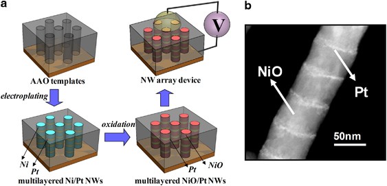
each NiO segment. EXPERIMENTAL PROCEDURES Schematic illustrations of the fabricated multilayered NiO/Pt nanowire-based devices are shown in Figure 1a. First, the anodic aluminum oxide (AAO)
templates were prepared by two-step anodization of Al sheets.26 The multilayered Ni/Pt nanowires were then prepared within the AAO templates by cyclic alternate electrodeposition in a
sulfate bath containing NiSO4·6H2O (2 M), H2PtCl6 (0.002 M) and H3BO3 (0.5 M). The detailed experimental procedures were reported in Huang _et al._25 After electroplating, 10 wt% H3PO4 was
used to enlarge the pore size of AAO, which can increase the empty space between nanowires and AAO so that oxygen can react with the nanowires during the subsequent annealing process.
Nanowires were subsequently annealed in air for 6 h at 800 °C to obtain multilayered NiO/Pt nanowires. The Pt top electrode with a thickness of 60 nm and a diameter of 200 μm was deposited
by sputtering using a shadow mask for the resistive switching measurements of nanowire arrays. The aluminum sheet below the AAO template was used as the grounded bottom electrode. To
construct single nanowire devices, the nanowires were liberated by dissolving AAO with 5 wt% NaOH. Next, the nanowires were collected by centrifugation and redispersed into isopropanol. The
nanowire suspension was then transferred onto a heavily doped _n_-type Si substrate with a thermally grown 500-nm-thick SiO2 layer. We used electron beam lithography and the lift-off process
to define the electrode patterns on the substrate, followed by a deposition of Pt/Ti (50 nm/150 nm) using evaporation. The resistive switching measurements were performed by using a
Keithley 4200 semiconductor characterization system. This single nanowire device was also studied in the configuration of a planar nanowire back-gate field-effect transistor device with
metal contacts functioning as source and drain electrodes, and a thermally grown 500-nm-thick SiO2 layer as the back gate. The field-effect characteristics were measured and evaluated.
RESULTS AND DISCUSSION A pore diameter of 70 nm and interpore distances of 90 nm were obtained with as-made well-ordered AAO templates that defined the diameter of nanowires and the number
of nanowires connected in parallel under a single Pt electrode. X-ray diffraction patterns of the annealed samples show that multilayered Ni/Pt nanowires completely transform to multilayered
NiO/Pt nanowires.25 The image of a single multilayered NiO/Pt nanowire obtained with a high-angle annular dark-field transmission electron microscope is shown in Figure 1b. The multilayered
NiO/Pt NWs are polycrystalline with thicknesses of each NiO and Pt segment of ∼50 and 10 nm, respectively. When alternating electrodeposition is repeated for 100 cycles, a single
multilayered nanowire can be considered as 100 NiO cells connected in series. We measured the resistance-switching characteristics in multilayered NiO/Pt nanowire arrays containing ∼106
nanowires in a parallel arrangement estimated by the areal density of AAO and the diameter of the top electrode (200 μm). As each nanowire contains ∼100 NiO cells in series, the total number
of resistive switching cells is estimated to be 108. Before conducting regular measurements, a relatively large voltage of ∼15 V is used to initialize the device27 for the subsequent
resistive switching. Figure 2a shows typical current–voltage (_I_–_V_) curves of the multilayered NiO/Pt nanowire arrays in either unipolar or bipolar operations with a compliance current of
0.1 mA. Switching from the low-resistance ‘ON’ state to the high-resistance ‘OFF’ state (RESET process) occurs at the reset voltages _V_RESET=1.15 V and _V_RESET=−1.20 V in the unipolar
(1→2) and the bipolar (1→3) operations, respectively, whereas the resistance transition from the HRS to LRS (SET process) occurs at a higher voltage _V_SET=3.25 V. The resistive switching
characteristics indicate that nonpolar switching between the HRS and LRS is achievable regardless of voltage polarity. Similar behaviors have been observed in some thin-film systems,9, 28
suggesting the conducting behavior of nanowire arrays may be related to the energy-assisted rupture of conducting paths. This voltage-induced resistance change is not observed in the blank
AAO matrix with voltage sweeping to 18 V (see Supplementary Information S1). Therefore, we confirm that this reversible resistive switching behavior is contributed only by the multilayered
NiO/Pt nanowires. This resistive switching behavior is highly reproducible in either unipolar or bipolar operations with a resistance ratio (HRS/LRS) as high as 105. Such an extraordinary
HRS/LRS ratio can be sustained without significant degradation at a reading voltage of 0.5 V for at least 60 cycles. A retention of ∼104 s was observed, similar to the reported value for NiO
cells29 (see Supplementary Information S2). The distribution of switching voltages for millions of nanoscale cells in the nanowire-array devices, shown in Figure 2b, is comparable to or
even better than the reported values in NiO nanowire devices24 and thin-film devices30 in which distributions were obtained from a single cell. The conducting paths in nanowires are strongly
confined due to the reduced lateral dimension. The inserted Pt layers serve as intermediate effective electrodes and allow the confined conducting paths to be reproducibly triggered by
electric fields. In consequence, the switching voltages are substantially reduced with sharper distributions.25 Note that very few works have reported multilevel effects in nanoscale cells,
especially in nanowire-based cells, mainly because the broadened distribution of the switching fields may mask the well-defined resistive states and result in irreproducible switching among
them. With the narrow distribution of switching voltages, clear multilevel switching is observed in our multilayered NiO/Pt nanowire arrays, as shown in Figure 2c. Multilevel states are
achieved by both unipolar and bipolar operations. The resistance state is set to the LRS (state ‘1’) first, and then voltage pulses with an amplitude of 5 V and a duration of 20 ns are
applied to the multilayered nanowire devices. It is remarkable that by applying sequential voltage pulses, we can produce a series of intermediate resistance states (labeled as state ‘2’ to
state ‘4’) and the HRS (state ‘0’) at the end. By applying a relatively large voltage pulse of 15 V, the device is brought from the HRS (state ‘0’) to the LRS (state ‘1’) again, and the
cycle is completed. The pulse-induced multilevel memory effect is reproducible, as shown in Figure 2d. It is worth emphasizing that the five resistance states presented above are not the
maximum limit but are given as an example. Because of the extremely large resistance ratio of 105, more resistance states can be deployed during design optimization. In most reported
multilevel memory effects generated by varying compliance currents or reset voltages, the multiple resistance states are believed to arise from the change in the number or sizes of the
conduction filaments.18, 19, 20 A gradual decrease in resistance is typically observed during the RESET process, consistent with the presence of multistable states explained by the filament
model. It is important to stress that the operation required to reach these multiple resistance states always requires starting from either the HRS (varied compliance current) or the LRS
(varied reset voltages). However, in our nanowire arrays (Figure 2), transitions between multiple resistance states can be achieved without going back to either the HRS or LRS—possibly
indicating a rather different conduction mechanism. We start with a simple ‘binary-resistor’ model to explain the multilevel transitions induced by voltage pulses. The device consists of
_N_w nanowires in parallel and _N_l layers of conduction cells in series within each nanowire. When no conduction path is available, the resistance of a conducting cell (a NiO segment in our
samples) is high, denoted by _R_. The voltage pulses help the formation of the conduction path in a cell, and its resistance drops to a much smaller value denoted by _r_. In real samples,
one expects that the binary values _R_ and _r_ in each conducting cell should be different. However, if their variances are small, it is reasonable to approximate all cells with the same
binary resistances. Within the binary-resistance model, the LRS of the nanowire arrays exhibits the maximum conductance _G_max=_N_w/_N_l_r_, whereas the HRS shows the minimum conductance
_G_min=_N_w/_N_l_R_. The transport measurement starts with the LRS. On application of one voltage pulse, it generates a finite probability _p_ to flip the resistance of a cell from _r_ to
_R_. Suppose the binary-flip probability _p_ generated by one voltage pulse is small (several percentiles in our samples), the effect caused by _n_ successive voltage pulses is additive and
the resultant binary-flip probability is simply _np_. The finite binary-flip probability accounts for the inhomogeneous distribution of resistances in different cells and the total
conductance _G_ of the nanowire arrays can be computed by averaging overall possible configurations. The resistor ratio _R_/_r_ has a crucial role in generating multilevel resistive states
and can be extracted from experimental data directly. For example, by using d_V_/d_I_ at _V_=0.5 V in the _I_–_V_ curve shown in Figure 2a, we can obtain the resistance of the HRS and LRS.
As the measured resistance of the HRS and LRS represents the resistance with the total number of _R_ and _r_ resistors connected in series and in parallel, respectively, the resistor ratio
of _R_/_r_ can be estimated rather accurately by taking the resistance ratio of the HRS to the LRS. Voltage pulses cause conducting cells to be flipped to different resistive configurations
and the total conductance of the nanowire arrays _G_ is computed by averaging overall possible binary configurations (detailed derivations in Supplementary Information S3), Here, the
dimensionless conductance (normalized to the maximum conductance) for a nanowire with _k_ flipped conducting cells is , depending only on the resistor ratio _R_/_r_ governed by the binomial
probability distribution . Because of the large resistance ratio _R_/_r_, the exact formula for the total conductance takes the simple exponential form _G_/_G_max≈, as explained next. For
_k_≠0 terms, at least one conducting cell is flipped to high resistance _R_ and the corresponding conductance is negligibly small. Thus, the total conductance is dominated by the _k_=0 term
in summation and the exponential form emerges, . Now, we are ready to compare the theoretical prediction with the experimental data, as shown in Figure 3a. Impressive agreement is found with
_p_=1.9% for pulse numbers _n_=0,1,2,3, giving rise to four robust multilevel resistive states. Note that the disagreement for the _n_=4 case is expected, because the exponential form no
longer holds and all conducting channels are flipped, bringing the nanowire arrays to the HRS with the highest resistance. The schematic diagram of the proposed binary-resistor model is
shown in Figure 3b. Another set of experimental data obtained using voltage pulses with an amplitude of 12 V and a duration of 20 ns shows the same impressive agreement between experiment
and theory (Supplementary Information S4). The binary-resistor model certainly has its limitations. In our model, the transwire conduction from one wire to the other nearby wires is not
included. If the transwire conduction is important, the exponential suppression of the total conductance will be gone, because the current cannot be easily blocked. Judging from the
exponential decay of the total conductance observed in our samples, it is safe to say that the transwire conduction has a minor role here. In addition, because of the multilayer structure
separated by metallic insertion (Pt), the conduction path formation in each conducting cell (NiO) is rather simple. Therefore, the resistance is _R_ without a conduction path and _r_
(<<_R_) in the presence of a conduction path. Suppose we elongate the length of the conducting cell or enlarge the diameter of the nanowires, it is expected that the formation of
conduction paths will be more complex and that the simple binary-resistor approximation will fail eventually. Therefore, the multilayer structure in nanowires has a crucial role in making
the binary-resistor model a good approximation. To further verify the origin of the multilevels, we obtained _I_–_V_ curves of the multilayered NiO/Pt single nanowire and single-layered NiO
nanowire arrays. The resistive switching of the multilayered NiO/Pt single nanowire device under unipolar and bipolar operations (Supplementary Information S5) reveals similar results to
those of nanowire-array devices, as shown in Figure 2a. This clearly indicates the good uniformity of nanowires. On the basis of _I_–_V_ similarity, together with the narrow distributions of
switching voltages observed in the nanowire arrays (Figure 2b), we can exclude the possibility that the multistable states observed in millions of cells originate from the variations of
different nanowires. Furthermore, the resistive switching of single-layered NiO nanowire arrays revealed higher switching voltages and wider switching distributions than those of the
multilayered NiO/Pt nanowire arrays, as we reported previously.25 Notice that we do not observe the multilevel effect in either multilayered NiO/Pt single nanowire or single-layered NiO
nanowire arrays, no matter how we adjust the amplitude or duration of voltage pulses. As multilayered NiO/Pt single nanowire devices show similar _I_–_V_ curves to those of NiO/Pt nanowire
arrays but do not possess intermediate states, we can conclude that the multilevel does not exist in each NiO segment. The binary-resistor model not only explains the observed multilevel
effects in the multilayer NiO/Pt nanowire arrays but also provides the reasons why neither the NiO single-layered array nor the multilayered NiO/Pt single nanowire exhibits multiple
resistance states. In the single-layered NiO nanowire array, the wire length is long, leading to the presence of the various conduction paths; therefore, they cannot simply be treated as a
binary resistor. In the multilayered NiO/Pt single nanowire, just one unit flipping to high resistance will destroy the only conducting channel, and multiple resistance states are not
possible. The model indicates that our multilevel memory effect reproducibly occurs in millions of cells, distinct from the reported work for single-cell devices. Our design of the
multilayer nanowire arrays enables us to measure resistance switching between robust multiple resistance states controlled by voltage pulses and enjoys the flexibility of varying the number
of nanowires and the layers within each nanowire. Furthermore, our synthesis method provides a versatile approach to achieve multilevels. The multistate mechanism we report here is novel,
and the key is to estimate the minimum number of wires needed to achieve the robust multilevel resistive states. By standard statistical analysis of the binary distribution (detailed
derivations presented in Supplementary Information S6), the criterion for the minimum number of wires is where . For the sample reported here, _p_=1.9% and _N_l=100, giving rise to _P_0≈15%.
The criterion for the number of wires is _N_w>>8. The criterion can be relaxed further if we shorten the length of the nanowires, for example, to _N_l=50, and the criterion becomes
_N_w>>4. On optimization, it is thus expected that _N_w∼10 is large enough (_N_w∼106 in our current sample) to achieve robust multilevel resistive states. The smallest AAO diameter
reported in the literature is ∼15 nm,31 and thus a multilayered nanowire device with multilevel resistive switching can be achieved at the size of 150 nm. Now, we would like to go beyond the
phenomenological binary-resistor model and elaborate on the microscopic mechanism for resistance switching. To explain the valid conduction mechanism in nanowires, we first investigated the
temperature dependence of resistance at the LRS on a single multilayered NiO/Pt nanowire in the temperature range of 85–325 K. An exponential decay of resistance versus temperature reveals
typical carrier transport behavior in a semiconductor, as shown in Figure 4a, which can be fitted by a simple model as:32 The activation energy of _E_a=0.03 eV is obtained from the ln(R)
versus T−1 plot. The negative temperature coefficient and low _E_a value, close to that of the high-defect NiO thin films (0.01–0.7 eV), suggest that the conduction in LRS is associated with
hopping via defects.32 Compared with the temperature dependence of the LRS of the NiO nanowire array reported in Huang _et al._,25 the activation energy is similar, which indicates that the
inserted Pt layers in NiO nanowires behave mainly as electrodes and that the NiO segments maintain the original conduction mechanism. Bulk NiO is a well-known _p_-type semiconductor when it
is nonstoichiometric and Ni deficient (or there is an oxygen excess).33 To determine the conduction mechanism in nanowires, we use the planar field effect transistor structure to determine
the carrier type.34, 35 Figure 4b shows the electrical current as a function of gate voltage (_V_g) in the range from −2 to 2 V. The inset of Figure 4b shows an scanning electron microscopic
image of the corresponding back-gate field-effect transistor structure of the multilayered NiO/Pt nanowires with a SiO2 layer as the back gate oxide. Although the bias voltage is fixed, the
current is modulated with varying _V_g. The current amplitude with a negative _V_g is larger than that with a positive _V_g. This evidently indicates the _p_-type nature of multilayered
NiO/Pt nanowires. It was reported that the presence of oxygen vacancies is critical to the resistance switching of _n_-type metal oxides.12, 13 However, oxygen vacancies form the defect
states at deep energy levels in NiO so that electrons in the presence of oxygen vacancies are highly localized.36 In contrast, the energy level of Ni vacancies is near the valence band of
NiO, so holes are the dominant carrier.37, 38, 39 The field-effect transistor measurement also confirms that holes are the dominant carriers in our nanowires. Furthermore, it has been
reported that oxygen ions are more mobile compared with Ni ions under electric fields.40, 41 Therefore, the movement of oxygen ions under an electric field may have a crucial role in
resistance switching, even in _p_-type NiO.37, 38 In our multilayered NiO/Pt nanowire arrays, the applied electrical field causes the oxygen ions to drift toward the anode during the SET
process. The accumulated O2− ions result in highly nonstoichiometric NiO (O/Ni ratio>1) and increase the hole concentration locally near the anode side. When the applied field approaches
_V_SET, the conductive region may extend from the anode to the cathode. Thus, hopping conduction through percolated paths prevails, leading to the LRS (Figure 4c). For the bipolar RESET
process, with the opposite applied electrical field, O2− ions migrate back into the bulk oxide and then recombine with oxygen vacancies, leading to a reduced O/Ni ratio and hole
concentration; thus, the HRS is achieved. For the unipolar RESET process, the temperature is increased locally due to Joule heating, which accelerates the migration of O2− ions to suppress
the concentration gradient. No matter which operation (bipolar or unipolar) is performed, applied electric fields change the configuration of O2− ions, which in turn modulate the local hole
concentrations. When we apply a pulsed voltage to multilayered NiO/Pt nanowires, the resistance changes in each NiO segment are governed by the redistribution of oxygen ions and holes in
NiO. By simply applying different numbers of pulsed voltages, the induced energy perturbation may reconfigure the oxygen ions and locally switch NiO segments from the LRS to the HRS. The
intermediate state of resistance does not exist in each NiO segment. Instead, it results from averaging overall possible binary configurations for each NiO segment in the multilayered
nanowire array, which is distinct from the reported multilevel in a single cell. In summary, we demonstrate nonpolar resistance switching behavior in multilayered NiO/Pt nanowire arrays with
low switching voltages and robust multilevel memory effects. Our bottom-up method provides a versatile approach to understand and design the resistance switching in a large number of
nanoscale NiO/Pt cells and suits the study of a variety of material systems. In addition, we propose that resistance switching in these nanoscale cells correlates closely with the hopping
conduction of holes. The multistable resistance states can be reliably achieved by simply applying different numbers of subsequent voltage pulses. The multilevel memory effects are well
captured by a simple binary-resistor model. We anticipate that our finding may expedite the adoption of resistive memory by the memory industry. REFERENCES * Waser, R. & Aono, M.
Nanoionics-based resistive switching memories. _Nat. Mater._ 6, 833–840 (2007). Article CAS Google Scholar * Strukov, D. B., Snider, G. S., Stewart, D. R. & Williams, R. S. The
missing memristor found. _Nature_ 453, 80–83 (2008). Article CAS Google Scholar * Garcia, V., Fusil, S., Bouzehouane, K., Enouz-Vedrenne, S., Mathur, N. D., Barthelemy, A. & Bibes, M.
Giant tunnel electroresistance for non-destructive readout of ferroelectric states. _Nature_ 460, 81–84 (2009). Article CAS Google Scholar * Lee, M. J., Park, Y., Suh, D. S., Lee, E. H.,
Seo, S., Kim, D. C., Jung, R., Kang, B. S., Ahn, S. E., Lee, C. B., Seo, D. H., Cha, Y. K., Yoo, I. K., Kim, J. S. & Park, B. H. Two series oxide resistors applicable to high speed and
high density nonvolatile memory. _Adv. Mater._ 19, 3919–3923 (2007). Article CAS Google Scholar * Lee, M. J., Han, S., Jeon, S. H., Park, B. H., Kang, B. S., Ahn, S. E., Kim, K. H., Lee,
C. B., Kim, C. J., Yoo, I. K., Seo, D. H., Li, X. S., Park, J. B., Lee, J. H. & Park, Y. Electrical manipulation of nanofilaments in transition-metal oxides for resistance-based memory.
_Nano Lett._ 9, 1476–1481 (2009). Article CAS Google Scholar * Oka, K., Yanagida, T., Nagashima, K., Tanaka, H. & Kawai, T. Nonvolatile bipolar resistive memory switching in single
crystalline NiO heterostructured nanowires. _J. Am. Chem. Soc._ 131, 3434–3435 (2009). Article CAS Google Scholar * Oka, K., Yanagida, T., Nagashima, K., Kawai, T., Kim, J. S. & Park,
B. H. Resistive-switching memory effects of NiO nanowire/metal junctions. _J. Am. Chem. Soc._ 132, 6634–6635 (2010). Article CAS Google Scholar * Cagli, C., Nardi, F., Harteneck, B.,
Tan, Z. K., Zhang, Y. G. & Ielmini, D. Resistive-switching crossbar memory based on Ni-NiO core-shell nanowires. _Small_ 7, 2899–2905 (2011). Article CAS Google Scholar * Guan, W. H.,
Long, S. B., Liu, Q., Liu, M. & Wang, W. Nonpolar nonvolatile resistive switching in Cu doped ZrO2 . _IEEE Electron. Device Lett._ 29, 434–437 (2008). Article CAS Google Scholar *
Liu, M., Abid, Z., Wang, W., He, X. L., Liu, Q. & Guan, W. H. Multilevel resistive switching with ionic and metallic filaments. _Appl. Phys. Lett._ 94, 233106 (2009). Article Google
Scholar * Yang, Y. C., Pan, F., Liu, Q., Liu, M. & Zeng, F. Fully room-temperature-fabricated nonvolatile resistive memory for ultrafast and high-density memory application. _Nano
Lett._ 9, 1636–1643 (2009). Article CAS Google Scholar * Qi, J., Olmedo, M., Ren, J. J., Zhan, N., Zhao, J. Z., Zheng, J. G. & Liu, J. L. Resistive switching in single epitaxial ZnO
nanoislands. _ACS Nano_ 6, 1051–1058 (2012). Article CAS Google Scholar * Yang, J. J., Pickett, M. D., Li, X. M., Ohlberg, D. A. A., Stewart, D. R. & Williams, R. S. Memristive
switching mechanism for metal/oxide/metal nanodevices. _Nat. Nanotechnol._ 3, 429–433 (2008). Article CAS Google Scholar * Kim, D. C., Seo, S., Ahn, S. E., Suh, D. S., Lee, M. J., Park,
B. H., Yoo, I. K., Baek, I. G., Kim, H. J., Yim, E. K., Lee, J. E., Park, S. O., Kim, H. S., Chung, U. I., Moon, J. T. & Ryu, B. I. Electrical observations of filamentary conductions for
the resistive memory switching in NiO films. _Appl. Phys. Lett._ 88, 202102 (2006). Article Google Scholar * Chae, S. C., Lee, J. S., Kim, S., Lee, S. B., Chang, S. H., Liu, C., Kahng,
B., Shin, H., Kim, D. W., Jung, C. U., Seo, S., Lee, M. J. & Noh, T. W. Random circuit breaker network model for unipolar resistance switching. _Adv. Mater._ 20, 1154–1159 (2008).
Article CAS Google Scholar * Waser, R., Dittmann, R., Staikov, G. & Szot, K. Redox-based resistive switching memories - nanoionic mechanisms, prospects, and challenges. _Adv. Mater._
21, 2632–2663 (2009). Article CAS Google Scholar * Gao, B., Kang, J. F., Chen, Y. S., Zhang, F. F., Chen, B., Huang, P., Liu, L. F., Liu, X. Y., Wang, Y. Y., Tran, X. A., Wang, Z. R., Yu,
H. Y. & Chin, A. Oxide-based RRAM: unified microscopic principle for both unipolar and bipolar switching. _Tech. Digest Int. Electron Devices Meet._ 417–420 (2011). * Russo, U.,
Kamalanathan, D., Ielmini, D., Lacaita, A. L. & Kozicki, M. N. Study of multilevel programming in programmable metallization cell (pmc) memory. _IEEE Trans. Electron Devices_ 56,
1040–1047 (2009). Article CAS Google Scholar * Wang, S. Y., Huang, C. W., Lee, D. Y., Tseng, T. Y. & Chang, T. C. Multilevel resistive switching in Ti/CuxO/Pt memory devices. _J.
Appl. Phys._ 108, 114110 (2010). Article Google Scholar * Nagashima, K., Yanagida, T., Oka, K., Taniguchi, M., Kawai, T., Kim, J. S. & Park, B. H. Resistive switching multistate
nonvolatile memory effects in a single cobalt oxide nanowire. _Nano Lett._ 10, 1359–1363 (2010). Article CAS Google Scholar * Ahn, S.-E., Lee, M.-J., Park, Y., Kang, B. S., Lee, C. B.,
Kim, K. H., Seo, S., Suh, D.-S., Kim, D.-C., Hur, J., Xianyu, W., Stefanovich, G., Yin, H., Yoo, I.-K., Lee, J.-H., Park, J.-B., Baek, I.-G. & Park, B. H. Write current reduction in
transition metal oxide based resistance-change memory. _Adv. Mater._ 20, 924–928 (2008). Article CAS Google Scholar * Lee, B. & Wong, H. S. P. Fabrication and characterization of
nanoscale nio resistance change memory (RRAM) cells with confined conduction paths. _IEEE Trans. Electron Devices_ 58, 3270–3275 (2011). Article CAS Google Scholar * Lee, M. J., Ahn, S.
E., Lee, C. B., Kim, C. J., Jeon, S., Chung, U. I., Yoo, I. K., Park, G. S., Han, S., Hwang, I. R. & Park, B. H. A simple device unit consisting of all NiO storage and switch elements
for multilevel terabit nonvolatile random access memory. _ACS Appl. Mater. Interfaces_ 3, 4475–4479 (2011). Article CAS Google Scholar * Kim, S. I., Lee, J. H., Chang, Y. W., Hwang, S. S.
& Yoo, K. H. Reversible resistive switching behaviors in NiO nanowires. _Appl. Phys. Lett._ 93, 033503 (2008). Article Google Scholar * Huang, Y.-C., Chen, P.-Y., Chin, T.-S., Liu,
R.-S., Huang, C.-Y. & Lai, C.-H. Improvement of resistive switching in NiO-based nanowires by inserting pt layers. _Appl. Phys. Lett._ 101, 153106 (2012). Article Google Scholar *
Masuda, H. & Fukuda, K. Ordered metal nanohole arrays made by 2-step replication of honeycomb structures of anodic alumina. _Science_ 268, 1466–1468 (1995). Article CAS Google Scholar
* Sawa, A. Resistive switching in transition metal oxides. _Mater. Today_ 11, 28–36 (2008). Article CAS Google Scholar * Huang, H. H., Shih, W. C. & Lai, C. H. Nonpolar resistive
switching in the Pt/MgO/Pt nonvolatile memory device. _Appl. Phys. Lett._ 96, 193505 (2010). Article Google Scholar * Goux, L., Lisoni, J. G., Wang, X. P., Jurczak, M. & Wouters, D. J.
Optimized ni oxidation in 80-nm contact holes for integration of forming-free and low-power Ni/NiO/Ni memory cells. _IEEE Trans. Electron Devices_ 56, 2363–2368 (2009). Article CAS Google
Scholar * Kim, D. C., Lee, M. J., Ahn, S. E., Seo, S., Park, J. C., Yoo, I. K., Baek, I. G., Kim, H. J., Yim, E. K., Lee, J. E., Park, S. O., Kim, H. S., Chung, U. I., Moon, J. T. &
Ryu, B. I. Improvement of resistive memory switching in NiO using IrO2 . _Appl. Phys. Lett._ 88, 232106 (2006). Article Google Scholar * Martín, J., Manzano, V. C., Caballero-Calero, O.
& Martín-González, M. High-aspect-ratio and highly ordered 15-nm porous alumina templates. _ACS Appl. Mater. Interfaces_ 5, 72–79 (2013). Article Google Scholar * Austin, I. G. &
Mott., N. F. Polarons in crystalline and non-crystalline materials. _Adv. Phys._ 18, 41–102 (1969). Article CAS Google Scholar * Adler, D. & Feinleib, J. Electrical and optical
properties of narrow-band materials. _Phys. Rev. B_ 2, 3112–3134 (1970). Article Google Scholar * Fan, Z., Wang, D. W., Chang, P. -C., Tseng, W. -Y. & Lu, J. G. Zno nanowire
field-effect transistor and oxygen sensing property. _Appl. Phys. Lett._ 85, 5923–5925 (2004). Article CAS Google Scholar * Nagashima, K., Yanagida, T., Oka, K., Kanai, M., Klamchuen, A.,
Kim, J. S., Park, B. H. & Kawai, T. Intrinsic mechanisms of memristive switching. _Nano Lett._ 11, 2114–2118 (2011). Article CAS Google Scholar * Park, S., Ahn, H.-S., Lee, C.-K.,
Kim, H., Jin, H., Lee, H.-S., Seo, S., Yu, J. & Han, S. Interaction and ordering of vacancy defects in NiO. _Phys. Rev. B_ 77, 134103 (2008). Article Google Scholar * Yoshida, C.,
Kinoshita, K., Yamasaki, T. & Sugiyama, Y. Direct observation of oxygen movement during resistance switching in NiO/Pt film. _Appl. Phys. Lett._ 93, 042106 (2008). Article Google
Scholar * Kinoshtia, K., Okutani, T., Tanaka, H., Hinoki, T., Yazawa, K., Ohmi, K. & Kishida, S. Opposite bias polarity dependence of resistive switching in n-type Ga doped-ZnO and
p-type NiO thin films. _Appl. Phys. Lett._ 96, 143505 (2010). Article Google Scholar * Oka, K., Yanagida, T., Nagashima, K., Kanai, M., Xu, B., Park, B. H., Katayama, Y. H. & Kawai, T.
Dual defects of cation and anion in memristive nonvolatile memory of metal oxides. _J. Am. Chem. Soc._ 134, 2535–2538 (2012). Article CAS Google Scholar * Volpe, M. L. & Reddy, J.
Cation self-diffusion and semiconductivity in NiO. _J. Chem. Phys._ 53, 1117–1125 (1970). Article CAS Google Scholar * Atkinson, A. Transport processes during the growth of oxide films at
elevated temperature. _Rev. Mod. Phys._ 57, 437–470 (1985). Article CAS Google Scholar Download references ACKNOWLEDGEMENTS We thank the National Science Council, Taiwan, Republic of
China (contract number NSC 98-2221-E-007-041-MY3), and the Ministry of Economic Affairs, Taiwan, Republic of China (contract number MOEA 99-EC-17-A-08-S1-006), for financially supporting
this research. AUTHOR INFORMATION AUTHORS AND AFFILIATIONS * Department of Materials Science and Engineering, National Tsing Hua University, Hsinchu, Taiwan Yen-Chun Huang, Kuo-Feng Huang,
Tzu-Chi Chuang & Chih-Huang Lai * Institute of Electro-optical Science and Technology, National Taiwan Normal University, Taipei, Taiwan Po-Yuan Chen * Department of Physics, National
Tsing Hua University, Hsinchu, Taiwan Hsiu-Hau Lin * Department of Materials Science and Engineering, Feng Chia University, Taichung, Taiwan Tsung-Shune Chin * Department of Chemistry,
National Taiwan University, Taipei, Taiwan Ru-Shi Liu * Institute of Physics, Academia Sinica, Taipei, Taiwan Yann-Wen Lan & Chii-Dong Chen Authors * Yen-Chun Huang View author
publications You can also search for this author inPubMed Google Scholar * Po-Yuan Chen View author publications You can also search for this author inPubMed Google Scholar * Kuo-Feng Huang
View author publications You can also search for this author inPubMed Google Scholar * Tzu-Chi Chuang View author publications You can also search for this author inPubMed Google Scholar *
Hsiu-Hau Lin View author publications You can also search for this author inPubMed Google Scholar * Tsung-Shune Chin View author publications You can also search for this author inPubMed
Google Scholar * Ru-Shi Liu View author publications You can also search for this author inPubMed Google Scholar * Yann-Wen Lan View author publications You can also search for this author
inPubMed Google Scholar * Chii-Dong Chen View author publications You can also search for this author inPubMed Google Scholar * Chih-Huang Lai View author publications You can also search
for this author inPubMed Google Scholar CORRESPONDING AUTHOR Correspondence to Chih-Huang Lai. ADDITIONAL INFORMATION Supplementary Information accompanies the paper on the NPG Asia
Materials website SUPPLEMENTARY INFORMATION SUPPLEMENTARY INFORMATION (DOC 2345 KB) RIGHTS AND PERMISSIONS This work is licensed under a Creative Commons Attribution-NonCommercial-ShareAlike
3.0 Unported License. To view a copy of this license, visit http://creativecommons.org/licenses/by-nc-sa/3.0/ Reprints and permissions ABOUT THIS ARTICLE CITE THIS ARTICLE Huang, YC., Chen,
PY., Huang, KF. _et al._ Using binary resistors to achieve multilevel resistive switching in multilayer NiO/Pt nanowire arrays. _NPG Asia Mater_ 6, e85 (2014).
https://doi.org/10.1038/am.2013.81 Download citation * Received: 04 July 2013 * Revised: 29 October 2013 * Accepted: 07 November 2013 * Published: 14 February 2014 * Issue Date: February
2014 * DOI: https://doi.org/10.1038/am.2013.81 SHARE THIS ARTICLE Anyone you share the following link with will be able to read this content: Get shareable link Sorry, a shareable link is
not currently available for this article. Copy to clipboard Provided by the Springer Nature SharedIt content-sharing initiative KEYWORDS * binary-resistor * multilayered nanowires *
multilevel memory effect * NiO * nonpolar resistive switching


:max_bytes(150000):strip_icc():focal(742x607:744x609)/Hiker-Bright-Angel-Trail-01-052623-8e87927a10dd42048a1167885a367680.jpg)