- Select a language for the TTS:
- UK English Female
- UK English Male
- US English Female
- US English Male
- Australian Female
- Australian Male
- Language selected: (auto detect) - EN
Play all audios:
ABSTRACT The existence of polytypism in semiconductor nanostructures gives rise to the appearance of stacking faults which many times can be treated as quantum wells. In some cases, despite
of a careful growth, the polytypism can be hardly avoided. In this work, we perform an _ab initio_ study of zincblende stacking faults in a wurtzite InP system, using the supercell approach
and taking the limit of low density of narrow stacking faults regions. Our results confirm the type II band alignment between the phases, producing a reliable qualitative description of the
band gap evolution along the growth axis. These results show an spacial asymmetry in the zincblende quantum wells, that is expected due to the fact that the wurtzite stacking sequence (ABAB)
is part of the zincblende one (ABCABC), but with an unexpected asymmetry between the valence and the conduction bands. We also present results for the complex dielectric function, clearly
showing the influence of the stacking on the homostructure values and surprisingly proving that the correspondent bulk results can be used to reproduce the polytypism even in the limit we
considered. SIMILAR CONTENT BEING VIEWED BY OTHERS FIRST-PRINCIPLES INVESTIGATION OF POLYTYPIC DEFECTS IN INP Article Open access 16 November 2022 SLIDING VAN DER WAALS POLYTYPES Article 21
November 2024 PHONONS AS A PLATFORM FOR NON-ABELIAN BRAIDING AND ITS MANIFESTATION IN LAYERED SILICATES Article Open access 20 January 2022 INTRODUCTION Indium phosphide is a III-V
semiconductor that crystallizes in the zincblende (ZB) phase in bulk, but that shows the wurtzite (WZ) crystal structure for nanowires1. Actually, the symmetry of these low dimensional
structures can be controlled in great extent through the growth conditions2,3. Some works show a relation between phase purity and the nanowires radius4 while others state that the stacking
sequence of newly grown monolayers are influenced by the underlying monolayers5. As a result, the fine tuning of the growth conditions can give rise to superlattices of the two polytypes or
twin planes along the nanowire axis6,7. Another interesting subject is the study of the influence of the stacking faults on the nanowire properties what opens the possibility of engineering
them through a strict structural control8,9. On the theoretical side, some attempts have been made to estimate the band offset between the WZ and ZB regions in polytypic homostructures
mainly through the connection between bulk calculations10,11,12. Recently, the _K_ · _P_ method was extended to these homostructures13,14,15 demanding large unit cells for a good description
of the systems. A better understanding of the InP properties in real nanowire samples is essential to increase their potential as building blocks of nanoscale electronic and photonic
devices16,17. In order to improve this understanding, we present here _ab initio_ calculations of the electronic properties of WZ InP samples with stacking faults with the ZB symmetry. To
the best of our knowledge, it is the first time that a sample with stacking faults is modeled using the supercell approach. This gives rise to a more realistic description of the system than
using bulk results10,11,12. For example, with this approach, we can show how the band gap evolves along the growth axis, avoiding the artificial abrupt band offset commonly assumed at the
WZ-ZB interface10,11,12,13,14,15. Remembering that the ZB stacking faults can be hardly avoided when one wants to grow a pure WZ InP nanowire, in our model, the ZB regions are far from each
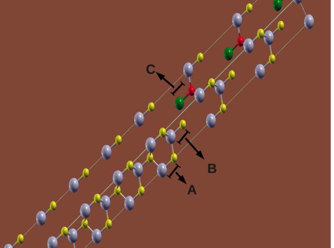
other, simulating a WZ InP sample with low density of narrow ZB layers. METHOD In order to model an InP sample in the WZ phase with a low density of ZB stacking faults, we built up an
hexagonal supercell with 15 layers of In and P atoms in the AB stacking sequence along the hexagonal _c_ axis of the WZ (4 atoms per layer, 60 atoms in total). On the top of this supercell,
we added three layers of In and P atoms using the ABC stacking sequence as along the [111]–direction of their ZB phase (6 atoms per layer, 18 atoms in total). In other words, we built up an
hexagonal supercell superimposing 15 InP WZ cells along their _c_ axis and over them we put 3 InP ZB cells where the cubic [111]–direction corresponds to the hexagonal _c_ axis. In Fig. 1 we
show an schematic representation of the interface between WZ and ZB regions in our supercell. The A, B and C layers whose stacking sequence defines the region symmetry are indicated. The C
layer that is present only in the ZB region has a different color scheme for clarity. We define a low density of ZB stacking faults as a case where the density of states (DOS) for the atoms
at the center of the WZ region reproduce the results obtained for the bulk WZ system. This condition intend to guarantee that the WZ bulk is reproduced at the middle between two neighboring
ZB regions. Our results show that this condition is achieved for our WZ region formed by 15 cells. On the other hand, since at the WZ-ZB interface the ABC sequence contains an AB region, we
need to use at least 3 ZB cells to assure the existence of a well defined ZB region. The _ab initio_ calculations have been performed using the “_Linearized Augmented Plane Wave method_”
(LAPW) as implemented in the Wien2k code18. Our basis functions were expanded up to _R__mt_ × _K__max_ = 6, where _R__mt_ is the smallest of the atomic “muffin-tin” radii and _K__max_ is the
magnitude of the largest _K_ vector for the plane wave basis functions. The atomic “muffin-tin” radii used here were 2.50 Bohr for In and 2.11 Bohr for the P atoms. We have employed the
modified Becke-Johnson exchange potential plus LDA correlation with its original parametrization (P-original)19,20. The energy separation for core and valence states was −6.0 Ry and the
spin-orbit coupling was taken into account during the calculation of the electronic properties. The only difference among the supercell and bulks calculations was the K-grid. For the total
energy and DOS calculations we employed K-grids with 12, 16 and 10 inequivalent points in the irreducible part of the Brillouin Zone (BZ) for the supercell, WZ and ZB bulks respectively. To
obtain the dielectric functions, denser grids were used (see below). The structural parameters used for the InP cells in the WZ and ZB phases were previously optimized for the bulk cases21.
The supercell were built up as described above and we considered two cases. In the first case, on top of the 15 optimized WZ cells, we added three ZB cells with the same WZ _a_ parameter.
The volume per atom obtained for the optimized ZB bulk was recovered through changes in the atomic distances along the _c_ axis. In the second case, we kept the same atomic distances along
the _a_ and _c_ axes found in the optimized WZ bulk and changed only the stacking sequence from AB to ABC. In both cases we got little forces on atoms along the _c_ axis, proving that we
were dealing with relaxed supercells. More specifically, these forces were always lower than 2.9 mRy/Bohr in the second structure and we have chosen this structure for our study. Besides
that, these results indicate that strain effects must have a minor role on the electronic properties of the supercell. RESULTS In Fig. 2 we show how the top of the valence band (blue
circles) and the bottom of the conduction band (red circles) evolve as a function of the atomic relative coordinate along the _c_ axis for two consecutive WZ InP supercells with ZB stacking
faults. To obtain these values, we compare the DOS per atom in the supercell with that of the bulk systems. We have observed that at the center of the WZ region, the corresponding bulk DOS
was reproduced at the band gap neighborhood. After that, we took from these central atoms the first derivative of the DOS at zero energy (top of the valence band) and at the gap energy of
the WZ bulk (bottom of the conduction band) and used them to determine how the two band extrema evolve along the supercell _c_ axis. Obviously, this is not a rigorous approach and Fig. 2
should be taken as a qualitative description. Despite of this, our results show a smooth transition between the WZ and ZB regions, what is a more realistic description than the commonly
assumed abrupt transition. As one can see, our results confirm the type II band alignment with holes concentrated at the WZ side of the WZ → ZB interface, while the electrons tend to be at
the ZB side of the ZB → WZ interface. This carriers spatial separation has a significant impact on the exciton recombination time8 and can be tuned through a strict control of the atomic
stacking sequence during the sample growth. We can also notice that the WZ → ZB and ZB → WZ are not equivalent due to the lack of mirror symmetry in the supercell and at the ZB region.
Finally, the shape of the band extrema evolution along the supercell _c_ axis is different for the valence and conductance bands. This is in a clear disagreement with the commonly modeled
type-II quantum wells, since, in our results, the conduction band profile looks like a square quantum well, while the valence band one is similar to a teeth saw quantum barrier. In Fig. 3,
we show the energy band gap (the difference between the two curves in Fig. 2) as a function of the atomic relative coordinates along the _c_ axis of the supercell. Here, it is important to
say that we have reduced the basis size when compared with our previous work21. The main change was the reduction of _R__mt_ * _K__max_ from 9 to 6 in order to decrease the computation time,
but keeping an acceptable level for results quality. In order to get a fair comparison with the bulk systems, we repeated the correspondent calculations with the same parameters used for
the supercell and we observed a reduction of approximately 23 meV in the bulk gaps when compared with the previously published values21. Here we obtain 1.470 eV and 1.373 eV for the WZ and
ZB gaps, respectively (dashed lines in Fig. 3). As previously commented, the calculated DOS at the center of the WZ region reproduced the WZ bulk results and we took their derivative as a
marker for the top of the valence band and the bottom of the conduction band. As a result, Fig. 3 shows the exact reproduction of the WZ bulk gap at the center of WZ supercell region. It is
also important to notice that the band gap, as the difference between the two curves in Fig. 2, reinforces the lack of mirror symmetry in the supercell with an almost linear behavior inside
the ZB region and very distinct profiles at the ZB → WZ and WZ → ZB interfaces. The impact of this asymmetry in the carriers localization and lifetime has been experimentally investigated8.
Figure 4 shows our projected density of states results for the WZ InP supercell with ZB stacking faults. We present the calculated values for _S_ (full red line), _P__x_ + _P__y_ (dashed
blue line) and _P__z_ (dotted black line) projections. As one can see, the WZ symmetry results are reproduced21. This means that the ZB region has practically no influence in the
polarization properties of the system as experimentally verified for the limit of low density of ZB stacking faults22. The convergence of the dielectric function was obtained with a more
dense K-grid. More specifically, we used 90, 198 and 104 inequivalent points in the irreducible part of the Brillouin Zone for the supercell, WZ and ZB bulks, respectively. In Fig. 5, we
present the real part of the complex dielectric permittivity as a function of the incident photon energy for the WZ InP supercell with ZB stacking faults (full green line with dots), WZ bulk
(dashed red line) and ZB bulk (dotted blue line). In the left panel (a), we consider light polarization in the _xy_ plane and, in the right panel (b), the polarization is taken along the
_z_ axis. As one can see, the ZB stacking faults have a small effect on the real part of the supercell dielectric function. The most noticeable deviations from the WZ results occur around 4
and 5 eV for both polarizations where the ZB values present pronounced dips. Nevertheless, it is important to show that a weighted average between the WZ and ZB bulk results perfectly fits
the supercell ones, even for the points where the supercell results exhibit the above mentioned deviation from the WZ values. The full line in both panels represent this average with weight
5 for WZ and 1 for ZB results (the rate between the number of bulk cells in the supercell). This is somehow surprising because we did not guarantee that the ZB region was able to reproduce
the correspondent bulk environment. It indicates that strain effects, that should differentiate the stacking faults from the bulk, must have a minor contribution to the supercell properties.
Beside this, it is expected that the interfaces between the symmetries have a significant role considering the narrow ZB region as reflected in the results for the conduction and valence
band edges evolving along the supercell _c_ axis (Figs 2 and 3). In conclusion, we can say that this somehow counterintuitive result indicates that approximations that consider abrupt
transitions between the phases can be suitable even in the case of low density of narrow stacking faults regions, opening the possibility of avoiding computationally expensive supercells
when modeling dielectric functions in homostructures. Figure 6 is equivalent to Fig. 5 but for the imaginary part of the dielectric function. Here, the main contribution of the ZB stacking
faults to the supercell results occurs in the energy interval from 4 to 6 eV for both polarizations, where the WZ and ZB bulk results are significantly different. Once more, the weighted
average results perfectly fit the supercell ones even in the energy range where the ZB stacking faults has the most important contribution. This corroborates our previous conclusion that,
surprisingly, bulk results can be used to reproduce supercell ones even for low densities of narrow stacking faults regions. CONCLUSIONS Our _ab initio_ analysis of a WZ InP system with ZB
stacking faults in the limit of low density of narrow ZB regions confirmed the type II band alignment between the phases, what can lead to the control of the exciton lifetime in this kind of
sample. Our results also show a reliable picture of the band gap smooth transition between the phases, with the ZB region presenting a linear dependence of the band gap with the position
along the supercell _z_ axis. Despite of this, the complex dielectric function results indicate the possibility of using bulk results to model the supercell systems. In other words, models
that consider abrupt transitions between the phases retain the essential characteristics of this kind of systems. ADDITIONAL INFORMATION HOW TO CITE THIS ARTICLE: Dacal, L. C. O. and
Cantarero, A. An _ab initio_ study of the polytypism in InP. _Sci. Rep._ 6, 33914; doi: 10.1038/srep33914 (2016). REFERENCES * Mattila, M., Hakkarainen, T., Mulot, M. & Lipsanen, H.
Crystal-structure-dependent photoluminescence from inp nanowires. Nanotechnology 17, 1580 (2006). Article CAS ADS Google Scholar * Bao, J., Bell, D. C. & Copasso, F. Optical
properties of rotationally twinned inp nanowire heterostructure. Nano Letters 8, 836 (2008). Article CAS ADS Google Scholar * Greenberg, Y., Kelrich, A., Calahorra, Y., Cohen, S. &
Ritter, D. Tapering and crystal structure of indium phosphide nanowires grown by selective area vapor liquid solid epitaxy. Journal of Crystal Growth 389, 103 (2014). Article CAS ADS
Google Scholar * Poole, P. J., Dalacu, D., Wu, X., Lapointe, J. & Mnaymneh, K. Interplay between crystal phase purity and radial growth in InP nanowires. Nanotechnology 23, 385205
(2012). Article CAS ADS Google Scholar * Priante, G., Harmand, J. C., Patriarche, G. & Glas, F. Random stacking sequences in III-V nanowires are correlated. Physical Review B 89,
241301(R) (2014). Article ADS Google Scholar * Xiong, Q., Wang, J. & Eklund, P. C. Coherent twinning phenomena: Towards twinning superlattices in III-V semiconducting nanowires. Nano
Letters 6, 2736 (2006). Article CAS ADS Google Scholar * Algra, R. E. et al. Twinning superlattices in indium phosphide nanowires. Nature 456, 369 (2008). Article CAS ADS Google
Scholar * Pemasiri, K. et al. Carrier dynamics and quantum confinement in type II ZB-WZ inp nanowire homostructures. Nano Letters 9, 648 (2009). Article CAS ADS Google Scholar *
Dobrovolsky, A. et al. Effects of polytypism on optical properties and band structure of individual Ga(N)P nanowires from correlative spatially resolved structural and optical studies. Nano
Letters 15, 4052 (2015). Article CAS ADS Google Scholar * Murayama, M. & Nakayama, T. Chemical trend of band offsets at wurtzite/zinc-blende heterocrystalline semiconductor
interfaces. Physical Review B 49, 4710 (1994). Article CAS ADS Google Scholar * Bechstedt, F. & Belabbes, A. Structure, energetics and electronic states of III-V compound polytypes.
J. Phys.: Condens. Matter 25, 273201 (2013). Google Scholar * Belabbes, A., Panse, C., Furthmüller, J. & Bechstedt, F. Electronic bands of III-V semiconductor polytypes and their
alignment. Physical Review B 86, 075208 (2012). Article ADS Google Scholar * Junior, P. E. F. & Sipahi, G. M. Electronic band structure of polytypical nanowhiskers. Physics Procedia
28, 72 (2012). Article ADS Google Scholar * Junior, P. E. F. & Sipahi, G. M. Band structure calculations of inp wurtzite/zinc-blende quantum wells. Journal of Applied Physics 112,
103716 (2012). Article ADS Google Scholar * Junior, P. E. F., Campos, T. & Sipahi, G. M. Interband polarized absorption in inp polytypic superlattices. Journal of Applied Physics 116,
193501 (2014). Article Google Scholar * Appell, D. Nanotechnology: Wired for success. Nature 419, 553 (2002). Article CAS ADS Google Scholar * Wang, J., Gudiksen, M. S., Duan, X.,
Cui, Y. & Lieber, C. M. Highly polarized photoluminescence and photodetection from single indium phosphide nanowires. Science 293, 1455 (2001). Article CAS ADS Google Scholar *
Blaha, P., Schwarz, K., Madsen, G. K. H., Kvasnicka, D. & Luitz, J. “_WIEN2k, An Augmented Plane Wave + Local Orbitals Program for Calculating Crystal Properties_” (Karlheinz Schwarz,
Techn. Universität Wien, Austria, 2001). * Tran, F. & Blaha, P. Accurate band gaps of semiconductors and insulators with a semilocal exchange-correlation potential. Physical Review
Letters 102, 226401 (2009). Article ADS Google Scholar * Koller, D., Tran, F. & Blaha, P. Improving the modified becke-johnson exchange potential. Physical Review B 85, 155109 (2012).
Article ADS Google Scholar * Dacal, L. C. O. & Cantarero, A. Ab initio electronic band structure calculation of inp in the wurtzite phase. Solid State Communications 151, 781 (2011).
Article CAS ADS Google Scholar * Gadret, E. G. et al. Valence-band splitting energies in wurtzite InP nanowires: Photoluminescence spectroscopy and ab initio calculations. Physical
Review B 82, 125327 (2010). Article ADS Google Scholar Download references ACKNOWLEDGEMENTS We would like to thank the São Paulo Research Foundation (FAPESP) for financial support
thorough grant: 2011/08513-1 and the Dirección General de Investigación Científica y Técnica (grants CSD2010-00044 and MAT2015-63955-R). The calculations were performed at the CENAPAD-SP
(National Center for High Performance Computing - São Paulo, Brazil), through the project UNICAMP/FINEP-MCT and at the supercomputer Tirant (University of Valencia), belonging to the Spanish
Network of Supercomputation. AUTHOR INFORMATION AUTHORS AND AFFILIATIONS * Instituto de Estudos Avançados, IEAv-CTA, PO Box 6044, São José dos Campos, 12228-970, SP, Brazil Luis C. O. Dacal
* Molecular Science Institute, University of Valencia, PO Box 22085, Valencia, E46071, Spain A. Cantarero Authors * Luis C. O. Dacal View author publications You can also search for this
author inPubMed Google Scholar * A. Cantarero View author publications You can also search for this author inPubMed Google Scholar CONTRIBUTIONS A.C. suggested the research and conceived the
supercell. L.C.O.D. performed the calculations. All authors analysed the results and reviewed the manuscript. ETHICS DECLARATIONS COMPETING INTERESTS The authors declare no competing
financial interests. RIGHTS AND PERMISSIONS This work is licensed under a Creative Commons Attribution 4.0 International License. The images or other third party material in this article are
included in the article’s Creative Commons license, unless indicated otherwise in the credit line; if the material is not included under the Creative Commons license, users will need to
obtain permission from the license holder to reproduce the material. To view a copy of this license, visit http://creativecommons.org/licenses/by/4.0/ Reprints and permissions ABOUT THIS
ARTICLE CITE THIS ARTICLE Dacal, L., Cantarero, A. An _ab initio_ study of the polytypism in InP. _Sci Rep_ 6, 33914 (2016). https://doi.org/10.1038/srep33914 Download citation * Received:
11 March 2016 * Accepted: 23 August 2016 * Published: 26 September 2016 * DOI: https://doi.org/10.1038/srep33914 SHARE THIS ARTICLE Anyone you share the following link with will be able to
read this content: Get shareable link Sorry, a shareable link is not currently available for this article. Copy to clipboard Provided by the Springer Nature SharedIt content-sharing
initiative