- Select a language for the TTS:
- UK English Female
- UK English Male
- US English Female
- US English Male
- Australian Female
- Australian Male
- Language selected: (auto detect) - EN
Play all audios:
ABSTRACT Plasmonics has established itself as a branch of physics which promises to revolutionize data processing, improve photovoltaics and increase sensitivity of bio-detection. A
widespread use of plasmonic devices is notably hindered by high losses and the absence of stable and inexpensive metal films suitable for plasmonic applications. To this end, there has been
a continuous search for alternative plasmonic materials that are also compatible with complementary metal oxide semiconductor technology. Here we show that copper and silver protected by
graphene are viable candidates. Copper films covered with one to a few graphene layers show excellent plasmonic characteristics. They can be used to fabricate plasmonic devices and survive
for at least a year, even in wet and corroding conditions. As a proof of concept, we use the graphene-protected copper to demonstrate dielectric loaded plasmonic waveguides and test
sensitivity of surface plasmon resonances. Our results are likely to initiate wide use of graphene-protected plasmonics. SIMILAR CONTENT BEING VIEWED BY OTHERS REAL-SPACE IMAGING OF ACOUSTIC
PLASMONS IN LARGE-AREA GRAPHENE GROWN BY CHEMICAL VAPOR DEPOSITION Article Open access 19 February 2021 LARGE-AREA NANOENGINEERING OF GRAPHENE CORRUGATIONS FOR VISIBLE-FREQUENCY GRAPHENE
PLASMONS Article 15 November 2021 HYBRIDIZATION OF GRAPHENE-GOLD PLASMONS FOR ACTIVE CONTROL OF MID-INFRARED RADIATION Article Open access 20 March 2024 INTRODUCTION Major obstacles to
practical applications of plasmonic devices1,2,3,4,5,6,7,8 are the absence of chemically stable, relatively cheap and easily manufacturable plasmonic materials, nanofabrication issues and
relatively high plasmonic losses9,10,11. Metals are usually chemically active and their surfaces easily oxidize degrading their plasmonic characteristics. The surface plasmon resonance
technique6 – the most successful plasmonic application so far – relies on noble metals and, in particular, gold. Ubiquitous in modern plasmonics gold is however not compatible with standard
silicon manufacturing processes, i.e., with complementary metal oxide semiconductor (CMOS) technology, due to very efficient diffusion of gold into silicon12. Various attempts have been made
to search for alternative plasmonic materials, such as metal alloys, semiconductors and even superconductors9,11,12. Recently, graphene emerged as a viable candidate for plasmonic
applications in the near infrared region of the spectrum10,13,14,15. However, a reliable and accessible plasmonic material for a wide range of practical applications remains wanted. The
problem of stability of a plasmonic material can be solved not only by searching for new candidates but also by finding a way to protect existing ones. For example, copper and silver exhibit
higher conductivity than gold and could be excellent plasmonic materials16,17,18 if only a way to protect them against oxidation is found19. To this end, a thin and inert coating
impermeable to oxygen, water and other corroding agents is required. The coating should be sufficiently thin to allow one to use enhanced plasmonic near-fields. Graphene may provide such a
coating20,21: it is one atom thick, mechanically strong, chemically inert and impenetrable to all gases and liquids22. Moreover, industrial-scale graphene sheets can now be grown by using
chemical vapour deposition (CVD) and then transferred onto various surfaces where they show strong and uniform adhesion20,23,24. There have already been reports in which graphene was
successfully employed to protect metals against corrosions and chemical reactions21,25,26. On the other hand, it has also been shown that copper with a graphene layer grown on top slowly
deteriorates due to defects and cracks in graphene and within several months the copper surface becomes even worse than without protection26. In this report, we investigate the viability of
graphene protection for plasmonic applications. We will concentrate on plasmonic geometries which utilize running plasmons and require a flat surface of metal with possible grooves and
dielectric and/or metal loaded structures with an ultimate goal to develop active plasmonic elements where graphene would provide an electric control of optical signals. In particular, we
show that copper films coated with transferred graphene exhibit surface plasmon resonance (SPR) with phase sensitivity to chemical binding events of several orders of magnitude better than
that of standard gold films. Graphene-protected copper does not display deterioration of SPR over the studied period of one year, despite subjecting our samples to water and other chemicals.
We have also fabricated a dielectric loaded surface plasmon polariton waveguide (DLSPPW)8 and demonstrate its successful functioning. The graphene coating provides not only a corrosion
barrier but also allows targeted (bio)functionalization of its surface. We illustrate the arising opportunities by using reversible graphene hydrogenation7 and measuring the corresponding
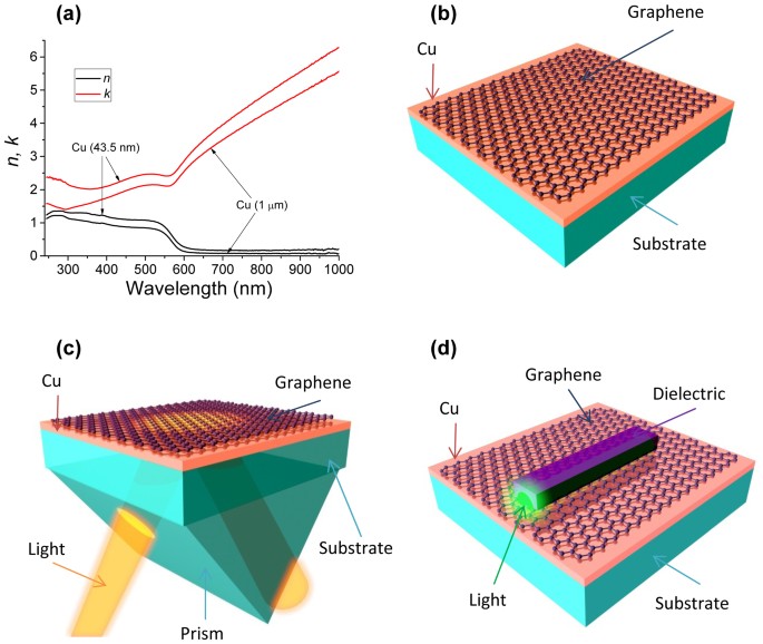
SPR sensitivity. RESULTS PREPARATION OF GRAPHENE-PROTECTED COPPER FILMS AND SPR MEASUREMENTS Copper thin films were made by electron-beam evaporation (Methods). Their morphology and optical
properties varied relatively little with the film thickness and employed substrate [see Fig. 1(a)]. All fresh-deposited samples showed excellent plasmonic characteristics that gradually
deteriorated with time, see below. To protect metal films against the deterioration, graphene was transferred on top using the wet-transfer procedure27. We used both mechanically exfoliated
graphene and graphene grown by CVD on copper (see Methods). A single layer of graphene transferred onto copper films [Fig. 1(b)] already showed excellent anticorrosion properties. However,
to avoid corrosion through occasional defects and cracks, the second graphene layer was deposited, so that overlaps between defects present in different layers became highly unlikely. We
could completely seal the metal surface with using more layers (3–5) but in practice two and often even one protective layers were found sufficient to preserve plasmonic properties for the
whole duration of our studies (~1 year), in contrast to graphene grown directly on copper26. To assess plasmonic properties of graphene-protected Cu, we have studied SPR by using the
Turbadar28-Kretschmann-Raether ATR geometry schematically shown in Fig. 1(c) (see details in Supplementary Information) and propagation of plasmon-polaritons in the DLSPPW geometry shown in
Fig. 1(d). The SPR for two Cu films (as fabricated; unprotected) are shown in Fig. 2(a) and (b). The data presented here are acquired using an unfocussed beam with a spot size of ~3.5 mm × 7
mm. For the Cu film of thickness _d_ = 43.5 nm the strongest resonance is observed at the angle θ_R_ = 49.5° for the wavelength λ_R_ = 588 nm; the prism refractive index _n_ was 1.5. The
minimum reflection for the SPR curve is Ψmin = 0.7° (for the ellipsometric parameter) which translates into the minimum intensity reflection Rmin = 5 × 10⁻⁴ (Fig. 2(b) and inset to Fig.
2(c)). The quality factors are _Q_ = 19 and 12, if extracted from the ellipsometric and reflection curves, respectively. Here _Q_ = λ_R_/Δλ_FWHM_ where λ_R_ is the resonance wavelength
corresponding to the SPR minimum and Δλ_FWHM_ is the full-width of the resonance at half-minimum of the resonance curve. These characteristics are better than those observed for Au films
with SPR at the same wavelength11,29, which can be attributed to the higher conductivity of copper and better morphology of our evaporated films. If left exposed to air or even placed in a
desiccator or low vacuum, the unprotected Cu samples have oxidized rapidly and the quality of SPR deteriorated; see Figs 2(c) and (d). After 30 days, the deepest SPR curve shifted to θ_R_ =
53° and the resonance minimum was observed at λ_R_ = 637 nm. The minimum reflection increased by a factor of 20 to Ψmin = 11.5° and the minimum intensity by a hundred times to Rmin = 4 ×
10−2, whereas the quality factor of the SPR curve dropped to _Q_ = 7 and 6 for the ellipsometric and reflection curves, respectively. In contrast, the samples protected by graphene did not
show any degradation of plasmonic characteristics and in the SPR curve even after half a year, see Fig. 2 and inset to Fig. 2(e). Moreover, graphene coating even improves the SPR quality, if
graphene is transferred within minutes after exposing Cu films to air (which is most probably connected to the decrease of oxidation time). In this case, Figs 2(e) and (f) show that for the
graphene-covered part of the same Cu film with _d_ = 43.5 nm, the deepest SPR occurs at θ_R_ = 49° and λ_R_ = 603 nm and exhibits Ψmin = 0.4° and Rmin = 3 × 10⁻⁴. _Q_ also increases to 20
and 13 for the ellipsometric and reflection curves, respectively. We stress that such small values of Rmin could not previously be achieved for Au films6, because of their morphology that
has proven difficult to improve and control30. At the same time, the reflectance Rmin is important for phase sensitive biosensing7 and special efforts have been made to improve it by using
collective plasmon resonances31 and topological darkness7. For completeness, Figure 3(a) provides a comparison of SPR curves measured in air for a fresh copper film, a film protected by one
graphene layer and a film protected by 2 graphene layers. Notice that the each graphene layer induces a small red shift of ~10 nm in the SPR position. It is also worth noting that graphene
does not decrease significantly the SPR resonance quality which comes from the fact that the enhanced SPR fields are perpendicular to the metal/graphene surface and hence do not produce
strong currents in the graphene sheet. SUITABILITY OF GRAPHENE-PROTECTED PLASMONICS FOR BIO-SENSING The main applications of SPR lie in biosensing which necessitates a wet environment.
Therefore, it is important to check that graphene is able to protect Cu films in water. Figure 3(b) shows a SPR curve for an unprotected film measured in water immediately after evaporation.
The SPR is observed at at θ_R_ = 60° and λ_R_ = 664 nm (_n_ = 1.8 in this case). The unprotected copper corrodes quicker in water than air and the SPR notably degrades in just 24 hours; see
Fig. 3(c). One can see that Ψmin increases from 1° to 21° and _Q_ drops from 19 to 9.5. On the contrary, graphene-protected films do not show deterioration in plasmonic properties in water
over the whole period of our studies. Figure 3(d) shows the typical SPR curves measured in water for a Cu film protected by a single layer of graphene. In water, graphene yields a red-shift
of 115 nm (which is connected with the usage of SPR resonance of longer wavelengths that becomes more pronounced after graphene transfer) with a simultaneous decrease in _Q_. At the same
time, the minimum reflection in the SPR curve drops to Ψmin = 0.3°. These changes can be well described by the Fresnel theory taking into account partial oxidation of the Cu films (see the
inset of Fig. 3(a), Fig. 4(c) and Methods). GRAPHENE PROTECTION OF SILVER FOR SPR APPLICATIONS The success of using graphene as a protective layer for Cu poses the obvious question whether
graphene coating can be employed for other metals. For example, silver is well known as one of the best possible plasmonic materials11 but it also notoriously known for its fast oxidation
and degradation. There were earlier attempts to apply graphene coating to safeguard plasmonic response of silver32 which found that the SPR response is stable in time but unfortunately it is
also mediocre. We have identified the reason for the invasive influence of graphene which lies with a graphene transfer protocol and developed a new graphene transfer procedure which solved
this problem (see Methods). As a result, we were able to protect Ag films with graphene without deteriorating the plasmonic properties of silver. Figures 3(e) and (f) show SPR curves for a
fresh Ag film and an Ag film covered with a monolayer of CVD graphene, respectively. One can see that graphene does not deteriorate the excellent SPR response of silver: the resonance
minimum changes from Ψmin = 0.3° for the freshly prepared Ag film, see Fig. 3(e), to Ψmin = 0.7° for graphene-protected Ag film, Fig. 3(f). We briefly compare the plasmon propagation length
in Au and graphene-protected Cu, Ag. Using optical constants extracted from ellipsometry, we estimate the following numbers for the propagation length assuming that the films are completely
flat: Au – 11.9 μm, Cu – 8.2 μm and Ag – 21.2 μm at the wavelength of 630 nm. The morphology of the films reduces these numbers to about 3–4 μm for our Au and graphene-protected Cu, while
the propagation length is about 10 μm for Ag. SPR SENSITIVITY OF GRAPHENE-PROTECTED PLASMONICS MEASURED WITH THE HELP OF GRAPHENE HYDROGENATION Having established that graphene coatings
efficiently protect plasmonic properties of copper and silver films, we have measured sensitivity of our SPR devices to binding chemicals, which is one of the most important parameters for
applications. To this end, we have chosen to use reversible graphene hydrogenation (Methods). Sensitivity to local environment (local refractive index) was also studied by utilizing
glycerol-water mixtures. Figs 4(a) and (b) show evolution of ellipsometric parameters when samples were exposed to atomic hydrogen, which led to partial hydrogenation of the graphene layer.
The hydrogenation ratio was monitored by Raman spectroscopy [inset of Fig. 4(b)] through the ratio of the intensity of the G and D peaks7. The hydrogenation level after 30 min of the
exposure was ≈17% which corresponds to the areal mass density σ of adsorbed hydrogen of ~10 pg/mm2. Accordingly, the mass sensitivity of our graphene-protected SPR sensor was δλ/σ ~0.15 nm
and δΔ/σ ~30° per pg/cm2 in terms of wavelength and phase measurements, respectively. Assuming a minimal detectable phase shift of 5 × 10⁻³ degrees33, we obtain the minimal detectable
adsorbed mass of ~0.2 fg/mm2. This detection limit is similar to that of plasmonic metamaterials with topological darkness7 and is 4 orders of magnitude better than the sensitivity achieved
for gold-based plasmonics6. Figures 4(c) and (d) illustrate the sensitivity of our SPR sensors for bio-applications where changes in local environment were mimics by replacing water (_n_ =
1.33) with a water-glycerol mixture (_n_ = 1.34). This charge results in a pronounced red-shift of the SPR, which translates into the wavelength sensitivity δλ/_δn_ ~5600 nm/RIU, where RIU
is the refractive index unit and δΔ/_δn_ > 2 × 10⁴ deg/RIU for the phase measurements. The former sensitivity is comparable with the theoretically envisaged sensitivity for gold-based SPR
sensors34 (~104 nm/RIU), whereas the latter is significantly better due to smaller reflection in the SPR minimum. It is worth mentioning that graphene and graphene oxide show good
biocompatibility35,36. APPLICATION OF GRAPHENE-PROTECTED COPPER FOR FABRICATION OF PLASMONIC WAVEGUIDES Finally, we show that graphene-protected copper can also be used in complex plasmonic
devices that require nanofabrications (for example, in waveguides and resonators). To this end, Figs 5(a) and (b) show schematics and an optical micrograph of a plasmon-polariton waveguide
that we have chosen as a test structure. The waveguide consists of a DLSPPW8 made on top of graphene-protected copper and the coupling and de-coupling gratings (see Methods). We excited the
waveguide by illuminating the coupling grating with a He-Ne laser (λ = 632.8 nm) and observed radiation coming out from the decoupling grating [Fig. 5(c)]. Figure 5(d) shows the dependence
of the transmitted light intensity as a function of the waveguide length. This yields the decay length for propagating waveguide modes of 10 μm, which suggests a strong contribution from
photonic modes. While the detailed mode analysis of the fabricated DLSPPW and its waveguiding characteristics along with the excitation efficiency is still to be carried out, the fact of
radiation transfer between the in- and out-coupling gratings is well established [Fig. 5(c)]. It is important to mention that Cu films without graphene protection would not survive the
nanofabrication procedures that take time and involve baking steps speeding up Cu corrosion. DISCUSSION To conclude, graphene-protected copper is a viable alternative to the conventional
noble metals in plasmonics applications. It is relatively cheap, stable, reproducible and high-quality plasmonic material that is suitable for nanofabrication and CMOS compatible. The
graphene-protected silver provides an exciting opportunity for applications which require low plasmonic losses. With the current rapid progress in CVD growth of hexagonal boron nitride and
other 2D crystals, we envisage that they can also be used as a quality protective coating for plasmonics. METHODS FILM DEPOSITIONS The copper films were produced by electron-beam evaporation
at a base pressure of about 10−7 mbar and growth rate of 0.3 nm/s (film thickness was monitored by calibrated quartz microbalance). As an electron-beam target, we used 99.99% Cu from
Sigma-Aldrich. A thin adhesion layer of Cr with thickness of about of 1.5 nm was evaporated onto a substrate before copper. Glass substrates of sizes 25 mm × 25 mm and thickness of 1 mm were
used for all the studied samples. The substrates were ultrasonically cleaned in heated acetone and isopropanol before deposition. In principle, CVD graphene can be grown directly on copper
films. However, we found that plasmonic properties of copper with CVD grown graphene are quite poor due to large surface roughness produced by CVD process. For this reason, in order to
produce graphene-protected copper we have used transfer procedure described below. This procedure (as well as CVD graphene) is inexpensive and can be easily automated. GROWTH OF CVD GRAPHENE
Cm-size graphene films were grown on Cu by using the CVD method24. A 25-μm thick Cu foil was placed inside a quartz tube and then heated to 1000°C with a H2 flow at rate of 20 cm3/min and a
pressure of 200 mTorr. To remove the native oxide layer, the foil was first annealed at 1000°C for 30 minutes. Then a gas mixture of H2 and CH4, with flow rates of 20 and 40 cm3/min,
respectively, was introduced into the chamber. CVD growth was performed at a pressure of 600 mTorr for 30 mins. Finally, the CVD chamber was rapidly cooled to room temperature in hydrogen
atmosphere. The grown films were predominantly single-layer graphene without many defects, verified by Raman spectroscopy. GRAPHENE TRANSFER PROCEDURE CVD-grown graphene was transferred on
to the target sample by using the following procedure7,27. First, graphene-on-Cu was covered by poly(methyl methacrylate) (PMMA) by using spin coating. Then the PMMA film with graphene layer
attached was isolated by chemically etching away the Cu foil. This PMMA-graphene film was then transferred onto the target copper films into a desired position under an optical microscope.
Finally, the PMMA layer was removed in acetone and the graphene surface was further cleaned by hydrogen annealing at 200°C for 60 mins. CVD graphene transfer on silver was performed as
follows. Graphene grown on copper foil was removed by etching the copper in 0.1 Mol ammonium persulfate for ~6 hours. Before etching, graphene was covered by 400 nm of PMMA with a tape
window cut out and placed on the PMMA so that the membrane can be mechanically moved after etching. The free floating graphene membrane was transferred to a clean dish of deionised (DI)
water for 5 min then to a second dish of DI water for a further 5 min to remove contamination from etchant solution. The graphene membrane was then taken out of the DI water and left to dry
in ambient conditions for about 10 min. A droplet of IPA was placed on the Ag substrate and the CVD graphene was placed on the IPA. The evaporating IPA helps the graphene adhere to the Ag
without the need for heating. (Ag can be easily oxidized in water and in air if the temperature is raised above ~50 degrees.) The sample was then placed in vacuum (~10−5 mbar) for about 30
min to pump away any remaining liquid from the interface and then the sample was heated to 50 degrees for half an hour to soften the PMMA. The PMMA was then dissolved in acetone, the sample
was rinsed with IPA and nitrogen dried. GRAPHENE HYDROGENATION In order to bind hydrogen to the graphene surface we used a cold hydrogen dc plasma at a low-pressure (~0.1 mbar) H2/Ar (1:10)
mixture. The plasma was ignited between Al electrodes. The level of hydrogenation was estimated by measuring the _D_ to _G_ peak intensity for hydrogenated samples registered by using a
Witec alpha 300R Raman spectrometer at a 514 nm excitation wavelength. A typical distance between hydrogen sites _L__D_ was calculated as , where λ is the wavelength measured in nanometers,
_I_(_G_) and _I_(_D_) are the intensities for the _G_ and _D_ Raman peaks of hydrogenated graphene7. This yields _L__D_≈10 nm after the 30 min hydrogenation. We assume that the size of
possible hydrogen clusters is smaller than the inter-cluster distance (~5 nm), which gives us an estimate of 17% hydrogenation after 30 min. It is worth noting that graphene hydrogenation is
a reversible process which can be reverted by a soft anneal7. FABRICATION AND CHARACTERIZATION OF DLSPPW Dielectric waveguide structures were produced by photolithography on
graphene-covered Cu films by using the negative tone photoresist ma-N 1405 from Micro-resist Technology. The substrate was pre-heated to 200°C in order to improve adhesion of the resist. We
used a 250-nm thick resist layer spin-coated on to the sample and patterned it with the Microtech Laserwriter LW405 system. The pattern was developed in ma-D 533/S developer and rinsed in
deionised water. Arrays of waveguides of width 1.0 μm and lengths 10 μm, 20 μm and 30 μm were fabricated. The pitch of coupling and de-coupling gratings was 1.2 μm; the grating ridge width
was 1.0 μm. To study light propagation in the waveguides, we illuminated the waveguide coupler with a 632.8 nm He-Ne laser at normal incidence by using a 100× objective lens to give a spot
size of ~500 nm. The incident laser power was ~0.5 mW. The transmitted light intensity was evaluated from calibrated CCD images. THEORY The reflection of our devices has been calculated by
using the Fresnel theory which takes into account light refraction on the right-angle prism and light reflection from a multi-layered structure facing air or glycol-water mixtures. The
thickness of copper and Cr layers were taken from microbalance measurements and checked by spectroscopic ellipsometry. The optical constants for all the layers were also measured by
spectroscopic ellipsometry. Graphene optical constants were taken in the analytical form and taking into account contributions from both intra and interband transitions. The only fitting
parameter was the thickness of an additional layer of copper oxide (<0.5 nm) that is formed immediately after the sample is taken out of the deposition chamber. REFERENCES * Barnes, W.
L., Dereux, A. & Ebbesen, T. W. Surface plasmon subwavelength optics. Nature 424, 824–830 (2003). Article ADS CAS PubMed Google Scholar * Maier, S. A. Plasmonics: Fundamentals and
Applications. (Springer, New York, 2007). * MacDonald, K. F., Sámson, Z. L., Stockman, M. I. & Zheludev, N. I. Ultrafast active plasmonics. Nature Photon. 3, 55–58 (2008). Article ADS
Google Scholar * Bozhevolnyi, S. I., Volkov, V. S., Devaux, E., Laluet, J.-Y. & Ebbesen, T. W. Channel plasmon subwavelength waveguide components including interferometers and ring
resonators. Nature 440, 508–511 (2006). ADS CAS PubMed Google Scholar * Atwater, H. A. & Polman, A. Plasmonics for improved photovoltaic devices. Nature Mater. 9, 205–213 (2010).
Article ADS CAS Google Scholar * Liedberg, B., Nylander, C. & Lundström, I. Biosensing with surface plasmon resonance - how it all started. Biosensors and Bioelectronics 10, i–ix
(1995). Article CAS PubMed Google Scholar * Kravets, V. G. et al. Singular phase nano-optics in plasmonic metamaterials for label-free single-molecule detection. Nature Mater. 12,
304–309 (2013). Article ADS CAS Google Scholar * Holmgaard, T. & Bozhevolnyi, S. I. Theoretical analysis of dielectric-loaded surface plasmon-polariton waveguides. Phys. Rev. B 75,
245405 (2007). Article ADS Google Scholar * Tassin, P., Koschny, T., Kafesaki, M. & Soukoulis, C. M. A comparison of graphene, superconductors and metals as conductors for
metamaterials and plasmonics. Nature Photon. 6, 259–264 (2012). Article ADS CAS Google Scholar * Grigorenko, A. N., Polini, M. & Novoselov, K. S. Graphene plasmonics. Nature Photon.
6, 749–758 (2012). Article ADS CAS Google Scholar * West, P. R. et al. Searching for better plasmonic materials. Laser & Photon. Rev. 4, 795–808 (2010). Article ADS CAS Google
Scholar * Naik, G. V., Shalaev, V. M. & Boltasseva, A. Alternative Plasmonic Materials: Beyond Gold and Silver. Adv. Mater. 25, 3264–3294 (2013). Article CAS PubMed Google Scholar *
Jablan, M., Buljan, H. & Soljačić, M. Plasmonics in graphene at infrared frequencies. Phys. Rev. B 80, 245435 (2009). Article ADS Google Scholar * Echtermeyer, T. et al. Strong
plasmonic enhancement of photovoltage in graphene. Nature Comm. 2, 458 (2011). Article ADS CAS Google Scholar * Koppens, F. H., Chang, D. E. & Garcia de Abajo, F. J. Graphene
plasmonics: a platform for strong light–matter interactions. Nano Lett. 11, 3370–3377 (2011). Article ADS CAS PubMed Google Scholar * Ehrenreich, H. & Philipp, H. Optical properties
of Ag and Cu. Phys. Rev. 128, 1622 (1962). Article ADS CAS Google Scholar * Robusto, P. & Braunstein, R. Optical measurements of the surface plasmon of copper. Phys. stat. sol. (b)
107, 443–449 (1981). Article ADS CAS Google Scholar * Futamata, M. Application of attenuated total reflection surface-plasmon-polariton Raman spectroscopy to gold and copper. Appl. Opt.
36, 364–375 (1997). Article ADS CAS PubMed Google Scholar * Tajima, N., Fukui, M., Shintani, Y. & Tada, O. In situ studies on oxidation of copper films by using ATR technique. J.
Phys. Soc. Japan 54, 4236–4240 (1985). Article ADS CAS Google Scholar * Geim, A. K. Graphene: Status and Prospects. Science 324, 1530–1534 (2009). Article ADS CAS PubMed Google
Scholar * Prasai, D., Tuberquia, J. C., Harl, R. R., Jennings, G. K. & Bolotin, K. I. Graphene: corrosion-inhibiting coating. ACS Nano 6, 1102–1108 (2012). Article CAS PubMed Google
Scholar * Bunch, J. S. et al. Impermeable atomic membranes from graphene sheets. Nano Lett. 8, 2458–2462 (2008). Article ADS CAS PubMed Google Scholar * Reina, A. et al. Large area,
few-layer graphene films on arbitrary substrates by chemical vapor deposition. Nano Lett. 9, 30–35 (2008). Article ADS Google Scholar * Li, X. et al. Large-area synthesis of high-quality
and uniform graphene films on copper foils. Science 324, 1312–1314 (2009). Article ADS CAS PubMed Google Scholar * Singh Raman, R. et al. Protecting copper from electrochemical
degradation by graphene coating. Carbon 50, 4040–4045 (2012). Article CAS Google Scholar * Schriver, M. et al. Graphene as a Long-Term Metal Oxidation Barrier: Worse Than Nothing. ACS
Nano 7, 5763–5768 (2013). Article CAS PubMed Google Scholar * Li, X. et al. Transfer of large-area graphene films for high-performance transparent conductive electrodes. Nano Lett. 9,
4359–4363 (2009). Article ADS CAS PubMed Google Scholar * Turbadar, T. Complete absorption of light by thin metal films. Proc. of the Phys. Soc. 73, 40 (1959). Article ADS CAS Google
Scholar * Zayats, A. V., Smolyaninov, I. I. & Maradudin, A. A. Nano-optics of surface plasmon polaritons. Phys. Rep. 408, 131–314 (2005). Article ADS CAS Google Scholar * Golan,
Y., Margulis, L. & Rubinstein, I. Vacuum-deposited gold films: I. Factors affecting the film morphology. Surface Science 264, 312–326 (1992). Article ADS CAS Google Scholar *
Kravets, V. G., Schedin, F. & Grigorenko, A. N. Extremely Narrow Plasmon Resonances Based on Diffraction Coupling of Localized Plasmons in Arrays of Metallic Nanoparticles. Phys. Rev.
Lett. 101, 087403 (2008). Article ADS CAS PubMed Google Scholar * Salihoglu, O., Balci, S. & Kocabas, C. Plasmon-polaritons on graphene-metal surface and their use in biosensors.
Appl. Phys. Lett. 100, 213110 (2012). Article ADS Google Scholar * Kabashin, A. V., Patskovsky, S. & Grigorenko, A. N. Phase and amplitude sensitivities in surface plasmon resonance
bio and chemical sensing. Opt. Express 17, 21191–21204 (2009). Article ADS CAS PubMed Google Scholar * Homola, J., Yee, S. S. & Gauglitz, G. Surface plasmon resonance sensors:
review. Sensors and Act. B: Chem. 54, 3–15 (1999). Article CAS Google Scholar * Pinto, A. M. et al. Biocompatibility of poly (lactic acid) with incorporated graphene-based materials.
Colloids and Surfaces B: Biointerfaces 104, 229–238 (2013). Article CAS PubMed Google Scholar * Wang, K. et al. Biocompatibility of graphene oxide. Nanoscale Res. Lett. 6, 1–8 (2011).
ADS Google Scholar Download references ACKNOWLEDGEMENTS We are grateful for the support by SAIT GRO Program and EPSRC grant EP/K011022/1. Y.-J. Kim was supported by the Global Research
Laboratory Program (2011-0021972) of the Ministry of Education, Science and Technology, Korea. The support of the Graphene Flagship project is acknowledged. AUTHOR INFORMATION AUTHORS AND
AFFILIATIONS * School of Physics and Astronomy, University of Manchester, Manchester, M13 9PL, UK V. G. Kravets, R. Jalil, Y.-J. Kim, D. Ansell, D. E. Aznakayeva, B. Thackray, L. Britnell,
B. D. Belle, F. Withers, K. S. Novoselov, A. K. Geim & A. N. Grigorenko * Department of Chemistry, College of Natural Sciences, Seoul National University, Seoul, 151-747, Korea Y.-J. Kim
* Institute of Technology and Innovation (ITI), University of Southern Denmark, Niels Bohrs Allé 1, DK-5230, Odense M, Denmark I. P. Radko, Z. Han & S. I. Bozhevolnyi Authors * V. G.
Kravets View author publications You can also search for this author inPubMed Google Scholar * R. Jalil View author publications You can also search for this author inPubMed Google Scholar *
Y.-J. Kim View author publications You can also search for this author inPubMed Google Scholar * D. Ansell View author publications You can also search for this author inPubMed Google
Scholar * D. E. Aznakayeva View author publications You can also search for this author inPubMed Google Scholar * B. Thackray View author publications You can also search for this author
inPubMed Google Scholar * L. Britnell View author publications You can also search for this author inPubMed Google Scholar * B. D. Belle View author publications You can also search for this
author inPubMed Google Scholar * F. Withers View author publications You can also search for this author inPubMed Google Scholar * I. P. Radko View author publications You can also search
for this author inPubMed Google Scholar * Z. Han View author publications You can also search for this author inPubMed Google Scholar * S. I. Bozhevolnyi View author publications You can
also search for this author inPubMed Google Scholar * K. S. Novoselov View author publications You can also search for this author inPubMed Google Scholar * A. K. Geim View author
publications You can also search for this author inPubMed Google Scholar * A. N. Grigorenko View author publications You can also search for this author inPubMed Google Scholar CONTRIBUTIONS
A.N.G. and A.K.G. conceived the idea. V.G.K., R.J., Y.-J.K., B.D.B., D.A., F.W. made the devices. V.G.K., B.T., L.B., K.S.N., A.N.G., A.V.K. modified samples and performed measurements.
I.P.R., Z.H., S.I.B. designed waveguides. D.E.A. performed calculations. All the authors contributed to discussion of the project. A.N.G. guided the project. ETHICS DECLARATIONS COMPETING
INTERESTS The authors declare no competing financial interests. ELECTRONIC SUPPLEMENTARY MATERIAL SUPPLEMENTARY INFORMATION supplementary information RIGHTS AND PERMISSIONS This work is
licensed under a Creative Commons Attribution-NonCommercial-NoDerivs 4.0 International License. The images or other third party material in this article are included in the article's
Creative Commons license, unless indicated otherwise in the credit line; if the material is not included under the Creative Commons license, users will need to obtain permission from the
license holder in order to reproduce the material. To view a copy of this license, visit http://creativecommons.org/licenses/by-nc-nd/4.0/ Reprints and permissions ABOUT THIS ARTICLE CITE
THIS ARTICLE Kravets, V., Jalil, R., Kim, YJ. _et al._ Graphene-protected copper and silver plasmonics. _Sci Rep_ 4, 5517 (2014). https://doi.org/10.1038/srep05517 Download citation *
Received: 15 April 2014 * Accepted: 13 June 2014 * Published: 01 July 2014 * DOI: https://doi.org/10.1038/srep05517 SHARE THIS ARTICLE Anyone you share the following link with will be able
to read this content: Get shareable link Sorry, a shareable link is not currently available for this article. Copy to clipboard Provided by the Springer Nature SharedIt content-sharing
initiative