- Select a language for the TTS:
- UK English Female
- UK English Male
- US English Female
- US English Male
- Australian Female
- Australian Male
- Language selected: (auto detect) - EN
Play all audios:
ABSTRACT Multi-valued logic gates, which can handle quaternary numbers as inputs, are developed by exploiting the ballistic transport properties of quantum point contacts in series. The
principle of a logic gate that finds the minimum of two quaternary number inputs is demonstrated. The device is scalable to allow multiple inputs, which makes it possible to find the minimum
of multiple inputs in a single gate operation. Also, the principle of a half-adder for quaternary number inputs is demonstrated. First, an adder that adds up two quaternary numbers and
outputs the sum of inputs is demonstrated. Second, a device to express the sum of the adder into two quaternary digits [Carry (first digit) and Sum (second digit)] is demonstrated. All the
logic gates presented in this paper can in principle be extended to allow decimal number inputs with high quality QPCs. SIMILAR CONTENT BEING VIEWED BY OTHERS REDUCING CNOT COUNT IN QUANTUM
FOURIER TRANSFORM FOR THE LINEAR NEAREST-NEIGHBOR ARCHITECTURE Article Open access 27 May 2023 EFFICIENT BOSONIC NONLINEAR PHASE GATES Article Open access 23 February 2024 ELECTRON CASCADE
FOR DISTANT SPIN READOUT Article Open access 04 January 2021 INTRODUCTION The conductance of a quantum point contact (QPC) differs from that of a classical resistor due to the quantized
energy levels and ballistic transport in the conduction channel. As a result, the output conductance of a QPC is quantized by 0, 1, 2, 3, 4… × 2_e_2/_h_1,2, which provides an opportunity to
develop multi-valued logic gates that can handle more than just binary numbers as an input. Another interesting property of a QPC is that the series resistance of multiple QPCs is determined
solely by the QPC with highest resistance; the resistance of the other QPCs is irrelevant3,4. Such unconventional transport properties can be exploited to develop logic gates that are
fundamentally different from conventional logic gates based on an inverter. Recently, it has been reported that some basic logic operations such as AND, OR, NOT and SUM can be realized by
exploiting the conductance quantization in ‘quantized conductance atomic switch’ (QCAS)5,6. However, in QCAS, the transport is ballistic only at the atomic junction formed between two
electrodes of the device. Hence it is a little bit difficult to use QCAS devices to develop fully ballistic logic gates. In this paper, we report multi-valued logic gate devices, which can
fully exploit the ballistic nature of quantum transport. We report a logic gate that finds the minimum of two quaternary number inputs based on the quantum transport properties of QPCs in
series. The logic gate is scalable to allow multiple inputs, which makes it possible to find the minimum of multiple inputs in a single gate operation. The principle of a half-adder, which
finds the sum and carry of two quaternary numbers, is then demonstrated. Although the logic operations for quaternary number inputs were observed, all the logic gates presented in this paper
can in principle be extended to allow decimal number inputs with high quality QPCs. The logic gates presented in this work are expected to be useful for enhancing the sorting algorithms and
reducing the computation time significantly. RESULTS The total resistance of classical resistors in series is given by the sum of all resistors. On the other hand, the resistance of QPCs in
series is determined by the resistance of the QPC with the maximum resistance provided that the transport inside the QPCs is ballistic3,4. All other QPCs with lower resistances are
irrelevant. This can be expressed in terms of the conductance as _G_s = min[_G_1, _G_2, ….,_G__N_], where _N_ is the number of QPCs, _G_n is the conductance of the individual QPC and _G_s is
the conductance through the series QPCs, which is quantized by integer multiples of _G_0 = 2_e_2/_h_. Wharam et al.3 reported that the series resistance of two QPCs in series behaves as
predicted4. By exploiting this interesting phenomenon, a ‘minimum logic gate’ that finds the minimum value of inputs can be realized. In principle, the device with only two QPCs in series
can be used as a minimum-finding logic gate (MFLG). In practice, however, it is necessary to decouple two QPCs electrostatically so that the number of conducting channels in the QPCs can be
assigned independently without affecting the nearby QPC. A MFLG device, which employs three QPCs in series to decouple the two input QPCs electrostatically, was developed. The device was
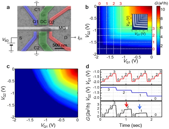
fabricated on a GaAs/AlGaAs heterostructure wafer (Fig. 1a and Method). Unlike the conventional QPCs, an extra middle gate (MG in the figure) was used in the gap of the QPC gates. By
applying a positive voltage on the middle gate, the depth of the potential well in the QPC could be made deeper and sharper, thereby making the sub-band energy spacing a few times larger (~7
meV) than that of a conventional QPC7. This helps to observe clear conductance quantization at 4.2 K and fabricate a clean 1-dimensional conducting channel along the gate by minimizing the
effects of unwanted potential fluctuations drawn by the ionized impurities in the modulation doping region. Fig.1b shows the conductance through the MFLG device measured as a function of the
voltage on the QPC1(Q1) and QPC2(Q2). A positive voltage (typically +0.25 V, just below the voltage that makes the current leak to the collector drains C1 and C2) on the decoupling gate DC
was applied to decouple Q1 and Q2 electrostatically. The device was totally pinched in the dark-blue region, whereas several constant-color (blue, light blue, green, yellow etc.) regions
showed quantized conductance (~1, 2, 3, 4 × 2_e_2/_h_ etc.). The inset is the derivative of the conductance ([(_dG_/_dV_Q1)2+(_dG_/_dV_Q2)2]1/2). The white vertical (horizontal) lines appear
as the number of conducting channels in Q1 (Q2) changes by the Q1 (Q2) gate voltage _V_Q1 (_V_Q2). The transition lines between the plateaus were almost vertical and horizontal, which means
that the two input QPCs barely affect each other. This allows the two inputs to be assigned independently. For comparison, Fig. 1c presents the same measurements for the device without a
decoupling gate (two 100 nm-wide QPCs in series separated by a 100 nm gap), which is similar to the results reported by Wharam et al.3. The transition voltages were determined by both the Q1
and Q2 voltages, which makes it difficult to use it as a logic gate device. The output conductance of 0, 1, 2, 3 × 2_e_2/_h_ can be considered as the output states 0, 1, 2 and 3, whereas
the QPC gate voltages that give the corresponding output conductance can be considered as the input states 0, 1, 2 and 3 (shown as white dashed lines in Fig. 1b). Fig. 1d shows the output
conductance of the device measured for various inputs of Q1 and Q2 (the inputs are changed as a function of time). The output conductance was plotted after subtracting the ~1.1 KΩ series
resistance. The figure shows that the output conductance of the device is determined only by the QPC with a smaller conductance, whereas the QPC with a higher conductance becomes irrelevant.
The output conductance representing the ‘2’ and ‘1’ output states, marked by the red and blue arrows, showed small conductance steps. The different series resistances (non-ballistic
resistance) of each QPC are responsible for the conductance steps, because the output conductance is determined only by the QPC with a smaller conductance. The height of the conductance step
was typically less than 10% of 2_e_2/_h_, which is small enough to distinguish between the two different output states. In principle, the minimum-finding logic gate can be used to determine
the minimum values for decimal numbers provided that the quantized plateaus of the QPCs are distinguishable up to the 10th conductance plateau. In principle, the device can operate at a
very high frequency, even though the actual measurement for this work was done at a very low frequency due to the limit of our experimental setup. In the ballistic transport regime, the
electron velocity of the 2 dimensional electron gas (2DEG) is determined by the Fermi velocity, which is given by and where _h_ is the plank constant, _m_* is the electron effective mass of
the 2DEG and _n_s is the carrier density of the 2DEG. Hence the Fermi velocity for an electron in a typical GaAs/AlGaAs 2DEG wafers (with electron density of 2 × 1011 cm−2) is around 2 × 10⁵
m/s. Considering that the typical channel length of our device is less than 1 μm, the time requires an electron to conduct through the device is around 5 × 10⁻¹² s. Therefore the device is
expected to work at a very high frequency (close to 1 THz), in principle. The device is fundamentally different from the conventional digital comparator, which has three output states
presenting (A > B), (A < B) and (A = B) not the minimum value itself. Having the minimum value as an output is a great advantage. For example, the number of input gates can be extended
easily by cascading the MFLG into a tree-like structure because the output of the MFLG can be coupled directly to the input of the next stage MFLG. Another way of extending the number of
input gates is simply to add more input gates in series provided that the ballistic transport is maintained in the device. Such a scheme will allow the minimum value among _n_ inputs to be
found by a single gate operation. In contrast, the conventional algorithm, which uses a conventional digital comparator, requires at least _n_-1 gate operations. In addition, a conventional
comparator can compare only binary numbers, whereas the MFLG can compare the decimal numbers in principle. This will allow significant enhancements of the sorting algorithms. Decoupling two
QPCs in series electrostatically make it possible to use the device as a MFLG. In the other extreme limit, where two QPCs are totally coupled electrostatically, the device can be used to add
two multi-valued inputs and generate the sum as an output. Fig. 2a shows the device, which can be used as an adder for two quaternary numbers. Two QPCs Q1 and Q2 (blue and red) composed of
two diagonally facing gates were used as the input gates of the adder. This makes both QPCs form constrictions almost in the same area (marked by a dashed circle). Fig. 2b shows the output
conductance (inset) and its derivative as a function of the Q1 and Q2 gate voltages. The output conductance is changed almost identically by Q1 and Q2. The white dashed lines were assigned
to represent the input states of the quaternary numbers. The output of the device was measured for various input states of Q1 and Q2, as shown in Fig. 2c. The output state is just a sum of
the input states, Q1 and Q2. This suggests that the confinement potential in the constriction is determined simply by the sum of the Q1 and Q2 gate voltages. A few different combinations of
gates as Q1 and Q2 were attempted and the best result was obtained for the combination shown in Fig. 2a. Adding two multi-digit numbers requires more than just creating the sum of two
single-digit numbers. For example, the sum of two quaternary numbers ranges from 0 to 6, which cannot be expressed as a single quaternary digit. Therefore, it is necessary to express the sum
into two quaternary digits [Carry (first digit) and Sum (second digit)], as summarized in the table in Fig 3d. The device shown in Fig. 3a was used to generate the Sum and Carry when the
input ranged from 0 to 7 (7 is also considered for the case when there is a Carry from a lower digit.). A positive voltage was applied to the B2 gate so that the current can flow to the
drain D2 while keeping the B1 gate closed. The bias voltage of −100 μV was applied to the source S and Q1 was used as an input gate while fixing the Q2 voltage to allow only 4 conducting
channels to pass through the QPC, as shown in Fig. 3b. The number of conducting channels passing through Q1 depends on the Q1 input gate voltage. When the number of conducting channels in Q1
is less than or equal to 4, it is expected that most of electrons passing through Q1 will also pass through Q2 provided that the transport is ballistic. For more than 4 channels in Q1, the
electrons carried by the extra channels will be rejected by Q2 and either deflected towards the D2 drain or back reflected towards the source. Fig. 3c shows the conductance measured at D1
and D2 for a range of Q1 input states. The input state of Q1 was assigned for the Q1 voltages, as shown as pink dashed lines in Fig. 3c. The conductance was plotted without compensating for
the series resistance of the device. The conductance of the plateaus measured at D1 were smaller than the corresponding integer multiples of 2_e_2/_h_. The conductance of the plateaus was
recovered to the expected values by compensating 2.5 KΩ series resistance. The conductance plateaus measured at D2 were approximately 0.63, 1.3 and 1.87 × _e_2/_h_ with a smaller step at
approximately 0.62 × _e_2/_h_. The reduction of the conductance step cannot be explained entirely by the series resistance of the device because the resistances of these plateaus (~ 41.1,
19.9 and 13.8 KΩ) were comparably larger than the series resistance of the device (~ 2 KΩ). A possible explanation for this reduction is that a considerable number of electrons are
back-reflected towards the source than deflected towards the D2 drain, which is reasonable for a ballistic device. Nevertheless, all the plateaus were distinguishable and could be used to
represent certain digital states. The table in Fig. 3d shows the output characteristics of the device. The output states at D1 and D2 were different from the ideal sum and carry for the
quaternary digit half-adder shown in the last two columns of the table. This discrepancy can be overcome by swapping the output of D1 and D2 using a conventional analog switch and comparator
if the output state at D1 is equal or larger than 4, which is not so difficult. This will swap the partial columns shaded in blue and red in the table to match the expected Sum and Carry (A
Carry of 4 rather than 1 can be corrected by dividing the signal with a simple resistor network). The overall operation will transform the input Q1, which ranges from 0 to 7, to two digit
quaternary numbers. Cascading the device shown in Figs. 2a and 3a (The two devices can be merged into a single device by attaching the B1 and Q2 gates of Fig 3a at the output of the device
shown in Fig. 2a) and swapping the partial output with an analog comparator and switch will produce a half-adder for quaternary numbers. In principle, the half-adder for the decimal input is
also possible with high quality QPCs. DISCUSSION In summary, this paper reports the principles of logic gates based on the ballistic transport properties of QPCs in series. All the logic
gates presented in this paper can be enhanced to handle decimal numbers for input with high quality QPCs. Recently, a QPC showing distinguishable plateaus up to 20 × 2_e_2/_h_ was reported8.
The logic gates presented in this paper will help to reduce the size and complexity of the device needed to perform the same logic operation with conventional logic gates. For example, a
conventional half-adder for binary numbers requires more than ten field-effect transistors (FET) at least. In contrast, the half-adder for multi-valued numbers presented in this paper
requires only a few QPCs and a few FETs for an analog switch (4 FETs) and a comparator (1 FET). The principles of the device rely on rather robust and simple physical phenomena, the
ballistic transport and electrostatic effect, which increases the likelihood of its adaption to real applications. The only impediment is to increase the working temperature of the QPC up to
room temperature. For the moment, the highest temperature to observe the reasonable conductance quantization in QPC is approximately 30 K9. Recently, the signature of conductance
quantization was observed at around 200 K in InAs nanowire transistor11, which looks promising for the future development of QPC working at room temperature. Although the principles of MFLG
and half-adder were presented only, we believe that different logic gates can also be developed based on the ballistic transport properties of QPCs in series. METHODS The devices were
fabricated on a conventional uniform doped GaAs/AlGaAs heterostructure grown by molecular beam epitaxy. The 2-dimensional electron gas was buried 77 nm below the surface of the GaAs/AlGaAs
heterostructure. The carrier density and mobility were 2.9 × 1011 cm−2 and 2.5 × 106 cm2/Vs, respectively, at 4.2 K. The widths of the all the gates were 100 nm except for the 300 nm wide
decoupling gate (DC). The gaps between the gates were kept to 100 nm. The device was cooled to 4.2 K with a positive voltage (+0.5 V) on all gates to reduce the random telegraph noise of the
device10. Therefore, the 2DEG beneath the gates were typically depleted below the gate voltage of approximately +0.3 V. The middle gate voltage was set to approximately +0.75 V to open the
conduction channels in the QPCs. The conductance was measured by applying a DC bias voltage of 100 μV to the source and measuring the drain current. REFERENCES * Van Wees, B. J. et al.
Quantized conductance of point contacts in a two-dimensional electron gas. Phys. Rev. Lett. 60, 848–850 (1988). Article ADS CAS Google Scholar * Wharam, D. A. et al. One-dimensional
transport and the quantization of the ballistic resistance. J. Phys. C 21, L209–L214 (1988). Article Google Scholar * Wharam, D. A. et al. Addition of the one-dimensional quantised
ballistic resistance. J. Phys. C 21, L887–L891 (1988). Article Google Scholar * Takagaki, Y. & Ferry, D. K. Double quantum point contacts in series. Phys. Rev. B 45, 13494–13498
(1992). Article ADS CAS Google Scholar * Terabe, K., Hasegawa, T., Nakayama, T. & Aono, M. Quantized conductance atomic switch. Nature 433, 47–50 (2005). Article ADS CAS Google
Scholar * Liao, Z.-M. et al. Resistive switching and metallic-filament formation in Ag2S nanowire transistors. Small 5, 2377–2381 (2009). Article CAS Google Scholar * Um, Y. J. et al.
Quantum point contact with large subband energy spacings. Appl. Phys. Lett. 100, 183502 (2012). Article ADS Google Scholar * Rössler, C. et al. Transport properties of clean quantum point
contacts. New J. of Phys. 13, 113006 (2011). Article ADS Google Scholar * Kristensen, A. et al. Conductance quantization above 30 K in GaAlAs shallow-etched quantum point contacts
smoothly joined to the background 2DEG. J. Appl. Phys. 83, 607–609 (1998). Article ADS CAS Google Scholar * Pioro-Ladrière, M. et al. Origin of switching noise in GaAs/Al_x_Ga1−_x_As
lateral gated devices. Phys. Rev. B 72, 115331 (2005). Article ADS Google Scholar * Chuang, S. et al. Ballistic InAs Nanowire Transistors. Nano Letters 13, 555–558 (2013) Article ADS
CAS Google Scholar Download references ACKNOWLEDGEMENTS The authors wish to thank M. Heiblum for the experimental support (access to experimental facilities and advice). This study was
supported by the Korea Research Institute of Standards and Science (KRISS) and the Basic Science Research Program through the National Research Foundation of Korea (NRF) funded by the
Ministry of Education (NRF-2013R1A1A2010792). AUTHOR INFORMATION AUTHORS AND AFFILIATIONS * Department of Physics, Pusan National University, 609-735, Busan, Republic of Korea M. Seo, C.
Hong, S.-Y. Lee & Y. Chung * Korea Research Institute of Standard and Science, 306-600, Daejeon, Republic of Korea N. Kim * Department of Condensed Matter Physics, Weizmann Institute of
Science, 76100, Rehovot, Israel H. K. Choi, V. Umansky & D. Mahalu * School of Electronics Engineering, Kyungpook National University, 702-701, Daegu, Republic of Korea S.-Y. Lee Authors
* M. Seo View author publications You can also search for this author inPubMed Google Scholar * C. Hong View author publications You can also search for this author inPubMed Google Scholar
* S.-Y. Lee View author publications You can also search for this author inPubMed Google Scholar * H. K. Choi View author publications You can also search for this author inPubMed Google
Scholar * N. Kim View author publications You can also search for this author inPubMed Google Scholar * Y. Chung View author publications You can also search for this author inPubMed Google
Scholar * V. Umansky View author publications You can also search for this author inPubMed Google Scholar * D. Mahalu View author publications You can also search for this author inPubMed
Google Scholar CONTRIBUTIONS M.S. and C.H. performed the experiments and equally contributed to this work. S.Y.L., N.K. and Y.C. planned the project. V.U. grew the wafers for the experiment
and D.M. and H.K.C. assisted in fabrication. Y.C. supervised the project and prepared the manuscript. All authors discussed the results and commented on the manuscript. ETHICS DECLARATIONS
COMPETING INTERESTS The authors declare no competing financial interests. RIGHTS AND PERMISSIONS This work is licensed under a Creative Commons Attribution-NonCommercial-ShareALike 3.0
Unported License. To view a copy of this license, visit http://creativecommons.org/licenses/by-nc-sa/3.0/ Reprints and permissions ABOUT THIS ARTICLE CITE THIS ARTICLE Seo, M., Hong, C.,
Lee, SY. _et al._ Multi-Valued Logic Gates based on Ballistic Transport in Quantum Point Contacts. _Sci Rep_ 4, 3806 (2014). https://doi.org/10.1038/srep03806 Download citation * Received:
10 October 2013 * Accepted: 23 December 2013 * Published: 22 January 2014 * DOI: https://doi.org/10.1038/srep03806 SHARE THIS ARTICLE Anyone you share the following link with will be able to
read this content: Get shareable link Sorry, a shareable link is not currently available for this article. Copy to clipboard Provided by the Springer Nature SharedIt content-sharing
initiative