- Select a language for the TTS:
- UK English Female
- UK English Male
- US English Female
- US English Male
- Australian Female
- Australian Male
- Language selected: (auto detect) - EN
Play all audios:
ABSTRACT On-going research is exploring novel energy concepts ranging from classical to quantum thermodynamics. Ferromagnets carry substantial built-in energy due to ordered electron spins.
Here, we propose to generate electrical power at room temperature by utilizing this magnetic energy to harvest thermal fluctuations on paramagnetic centers using spintronics. Our spin engine
rectifies current fluctuations across the paramagnetic centers’ spin states by utilizing so-called ‘spinterfaces’ with high spin polarization. Analytical and ab-initio theories suggest that
experimental data at room temperature from a single MgO magnetic tunnel junction (MTJ) be linked to this spin engine. Device downscaling, other spintronic solutions to select a transport
spin channel, and dual oxide/organic materials tracks to introduce paramagnetic centers into the tunnel barrier, widen opportunities for routine device reproduction. At present MgO MTJ
densities in next-generation memories, this spin engine could lead to ‘always-on’ areal power densities that are highly competitive relative to other energy harvesting strategies. SIMILAR
CONTENT BEING VIEWED BY OTHERS OXYGEN VACANCY-DRIVEN SPIN-TRANSFER TORQUE ACROSS MGO MAGNETIC TUNNEL JUNCTIONS Article Open access 07 January 2025 EMERGING FERROMAGNETIC MATERIALS FOR
ELECTRICAL SPIN INJECTION: TOWARDS SEMICONDUCTOR SPINTRONICS Article Open access 28 March 2025 OBSERVATION AND THEORETICAL CALCULATIONS OF VOLTAGE-INDUCED LARGE MAGNETOCAPACITANCE BEYOND
330% IN MGO-BASED MAGNETIC TUNNEL JUNCTIONS Article Open access 12 July 2021 INTRODUCTION A solar cell’s electronic potential landscape is crafted such that, when a photon is absorbed, the
resulting electron and hole (the absence of an electron) flow in opposite directions. Since they carry an electrical charge of opposite sign, this generates an electrical current. Two
low-temperature experiments1,2 have suggested that, by astutely designing the magnetic potential landscape of a quantum dot (QD) device, electrons with a spin ↑ or ↓ quantum property can
flow in opposite directions. This can generate electrical power if the spin ↑ and ↓ current channels are imbalanced, i.e. if the overall current is spin-polarized. This apparent current
imbalance, and the presence of QDs in both systems, are reminiscent of quantum thermodynamical experiments on single electron boxes, which have demonstrated how to harvest thermal
fluctuations3,4 and information5 to perform work at very low temperatures. These heat and information engines are driven by fluctuation-induced quantum tunneling on/off of QDs, with a
transmission asymmetry between left and right leads that can be energy-dependent due to the QD’s discrete energy levels6,7. A few reports have theoretically8 and experimentally (using
nitrogen vacancies in diamond9) taken into account the electron spin. Inspired by the report of Miao et al.2, and by recent progress in quantum thermodynamics3,4,5,6,7,8,9,10,11,12, we
propose that a spin-split paramagnetic (PM) quantum object can enable electrons with a spin ↑ or ↓ quantum property to flow in opposite directions if the transmission rates on either side of
the PM center are spin-dependent. Differing amplitudes in these transport spin channels generate a spontaneous current flow. Measurements across a single MgO magnetic tunnel junction,
backed by analytical and ab-initio theories, indicate that this spin engine can operate at room temperature. We discuss strategies to achieve routine device reproduction. Our work also
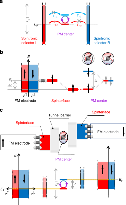
confirms the high transport spin polarization at room temperature of the ferromagnetic metal/molecule interface13 inferred from spectroscopy measurements14. RESULTS Figure 1a illustrates our
spin engine in the simplified case of a PM center, characterized by two effectively spin-split energy levels. To achieve a strongly spin-dependent transmission rate Γ, the PM center is
placed between spintronic selectors—materials systems that ideally favor only one transport spin channel while blocking the other. Examples include half metals15,16,17, 2D materials with
half-metallic properties18, a normal metal / ferromagnetic tunnel barrier19 bilayer, and the ferromagnetic metal/molecule interface13, also called a ‘spinterface’. The Fe/MgO system may also
constitute a spintronic selector given either a sufficient MgO thickness20 and/or the presence of oxygen vacancies21,22,23,24. A standard ferromagnetic metal (FM) would also work, albeit
with reduced efficiency. Due to this combination of spintronic selectors and spin-split PM states, a spin ↑(↓) electron may only depart the PM toward the left(right) electrode at the energy
of the PM center’s corresponding spin state. Hai et al.1 used a MnAs ferromagnetic metal with a conventional (~50%) spin polarization of conduction states, and applied a magnetic field to
spin-split their MnAs QDs and obtain power generation at 3K. It is unclear whether this experiment could have worked at higher temperatures. Miao et al.2 filtered the electron spin upon
transport across EuS ferromagnetic tunnel barriers at 1K, i.e. below its ordering temperature TC ~ 16.8 K. Here, spin splitting of the Al QD is induced by electronic coupling to one EuS
barrier. Reports indicate that several spintronic selector tracks include materials science candidates (e.g. the Fe/MgO MTJ class20,22, the half-metallic Co2FeAl17 or the ferromagnetic
tunnel barrier CoFe2O419) that can operate at/beyond room temperature (RT). To obtain RT electrical generation, and in the process demonstrate it to be a RT spintronic selector, we utilize
the spinterface13,14,25,26. This refers to a low energy bandwidth, low density of highly spin-polarized states that arise at room temperature from spin-polarized hybridization between the
highly degenerate electronic states of a FM metal such as Co and the few, energetically discrete states of molecules, including carbon atoms26. The spinterface is weakly conducting, and its
magnetic orientation naturally follows that of the FM metal. To date, only spin-polarized photoemission spectroscopy14,26 suggests that the spinterface may be a spintronic selector at RT. We
now utilize the case of the spinterface to illustrate several key considerations of how spintronic selectors and PM centers can interact to form the spin engine’s transport path. Upon
connecting the spinterface to the PM state (see Fig. 1a), spin-conserved quantum tunneling conditions the resulting spin-polarized landscape in the following significant ways. First, the
spinterface’s density of states (DOS) with a spatially oriented spin polarization generates a corresponding spintronic anisotropy in the PM state’s stochastic spin distribution27,28, thereby
deforming the PM’s Bloch sphere of spin states. This generates an energy difference Δ between the PM center’s spin states and increases the probability that an electron tunnel onto/off of
the PM if its spin is aligned to the spinterface’s spin referential (see Fig. 1b). The ensuing preferential charge flow for that spin channel effectively shifts2 the spinterface/FM metal’s
Fermi level by Δ_ϕ_ toward that spin state of the PM center. We are thus describing how the spinterface can modify a metal’s properties29, namely its Fermi level position, through an
additional mechanism. In a perfectly symmetric magnetic tunnel junction (MTJ) that implements spin-conserved tunneling between these two key ingredients—spinterfaces and a PM site—no net
current (I) should flow in the MTJ’s parallel (P) orientation of electrode magnetizations. However, in the MTJ’s antiparallel (AP) magnetic state (see Fig. 1a), the two FM electrode Fermi
levels are shifted away from one another, each toward the corresponding spinterface-selected spin state of the PM center. The resulting spontaneous bias voltage ΔV between the FM electrodes
thus scales with the amplitude of the spinterface’s spin polarization and the energy difference Δ between the PM center’s spin ↑ and ↓ states. Since an experimental MTJ cannot be exactly
symmetric, one may also anticipate a spontaneous bias, or current, in the MTJ’s P state, albeit of lower amplitude. To generate work, the spin engine harvests energy from the spin
fluctuations that are thermally induced on the PM center. This thermal spin state mixing on the PM center enables current to flow from one spinterface to the other, even against the built-in
ΔV in the MTJ’s AP magnetic state. The spin engine thus requires that Δ ≤ _k_BT, and thus a balance between the tunneling-induced energy shift Δ_ϕ_ of the spinterface state to the PM
center’s spin state and thermal fluctuations, as weighed by the spinterface’s spin polarization (see Fig. 1c). This thermal energy harvesting can be expected to cool the PM center.
Furthermore, the fully spin-polarized current flowing across the spinterface perturbs the FM ground state of the electrode through a spin accumulation-induced interfacial resistance30. The
resulting heat generation in the FM electrode must be dissipated for our spin engine to work. Finally, the spinterface’s low density of highly spin-polarized states may be beneficial to RT
operation. Indeed, it protects the energetically discrete PM spin states against thermal broadening from the FM electrodes. As discussed theoretically in Supplementary Notes 1 and 2, the
thermal fluctuations in current are rectified first upon transport from the FM electrode onto the spinterface, and furthermore upon transport from the spinterface onto the PM center’s spin
state. This, along with the spinterface’s high spin polarization, strongly dampens any energy smearing of the PM center’s discrete spin states. The resulting energetically sharp,
spin-polarized effective current path involving the striped DOS of the FM electrodes and spinterfaces is schematized in Fig. 1c by the yellow band. With the support of analytical and
ab-initio theories, we believe to have observed an experimental realization of this spin engine through measurements across a single MgO MTJ at room temperature (RT; see junction statistics
in Supplementary Note 3). As described hereafter, this MTJ integrates Co/C spinterfaces with nearly total spin polarization26, and paramagnetic C atoms31 on the oxygen vacancy sites of the
MgO tunnel barrier. Referring to Fig. 2a, we observe a negative tunneling magnetoresistance ratio, i.e. TMR = IP/IAP − 1 < 0, at V = +10 mV and T = 295 K through P/AP magnetic states that
are well controlled thanks to an IrMn pinning layer (see Methods). Figure 2b shows the I(H) data acquired at V = +5 mV. Over the ~350 s needed to ramp H down from −2000 Oe to ~0Oe, the MTJ
remains in a P magnetic state, with IP < 0 despite V > 0. In the MTJ’s AP state, IAP > 0 over ~310 s. The abrupt magnetic field dependence of the switch in sign of current clearly
shows that the current sign change originates from the change in the MTJ’s magnetic state, and not the magnetic field amplitude/sweep. Both IP and IAP exceed the maximum 500 pA possible
experimental offset by nearly 2 orders of magnitude (see Supplementary Notes 4 and 5). Thus, in this MTJ, the direction of static current flow can be reversed by simply switching the MTJ’s
spintronic state. Since the external magnetic field is static, and we do not expect a spin texture in our FM electrodes, a spin motive force explanation1,32,33 seems unlikely. In these and
our experiments, no explicit temperature difference between electrodes, or temperature gradient, is applied to the device, such that a spin caloritronics34 explanation, while possible, is
not obvious. We further discuss in the Methods and Supplementary Note 5 how photovoltage/photocurrent and conventional/spintronic thermovoltage17,35 artifacts can be excluded here. These
I(H) datapoints are confirmed through I(V) measurements at RT in the MTJ’s P and AP states (see Fig. 2c), which reveal the following features: (1) at V = 0, IP ≠ IAP ≠ 0, with an amplitude
that also exceeds any experimental offset by nearly 2 orders of magnitude; (2) a non-zero applied bias V leading to a measured I = 0 whose amplitude depends on the MTJ’s magnetic state; (3)
power generation above 0.1 nW whose bias dependence depends on the MTJ’s magnetic state, with a maximum current IAP ≈ −70 nA at V = +1.4 mV (see panel (c) inset using data from Supplementary
Fig. 5a; (4) bias-driven oscillations in current that depend on the MTJ’s P/AP magnetic state, and thus on spin-dependent transport; (5) a bias range for which IP and IAP are of opposite
sign, leading to TMR < −100%. These features of the 0 → +Vmax → −Vmax → +Vmax → −Vmax → 0 I(V) sweep are reproduced with high fidelity in Fig. 2c for another such sweep with differing
maximum applied bias Vmax and bias step (i.e. a differing effective bias sweep rate), as well as by additional datasets (see Supplementary Note 4). This eliminates any junction
instability/memristive/Joule heating explanation36. (6) The numerically derived junction conductance dI/dV of the data of Fig. 2c, shown in Fig. 2d, reveals spintronically determined
conductance jumps, and spectral features as low as 0.25 meV—despite the 2_k_BT ≈ 50 meV thermal smearing expected at 295 K—that are statistically beyond the error bar (see Fig. 2d inset and
Supplementary Note 6 for full dataset and error bars) thanks to an excellent signal-to-noise ratio. This spectral sharpness is also witnessed through a 300% TMR peak with a
full-width-half-max of ~1.3 meV (see Fig. 2e), which arises from a combination of local maxima(minima) in IP(IAP) at V = −3.5 mV. This non-optimized device’s spintronic performance at 295 K
rivals the 600% record for FeCoB/MgO-class MTJs—obtained through a 20-fold performance increase over 7 years37,38 — but since the Co electrodes cannot be _bcc_-oriented here20,39 (see
Methods), this spintronic performance cannot arise from symmetry filtering. Within a simple Jullière model20 interpretation of the TMR amplitude, and from our analytical theory presented
hereafter, this can be ascribed in part to the high transport spin polarization of the Co/C spinterface26 at RT. This spectral sharpness in magnetotransport features at RT despite the
expected thermal broadening, and the excellent signal-to-noise ratio, can be interpreted as an experimental signature of our spin engine at work. Indeed, according to quantum
thermodynamics4,7, the harvesting of spin fluctuations on the PM centers is expected to lower their temperature. From _k_BT ≈ 0.25 meV, we estimate an effective electronic temperature of the
PM centers of 3 K. This cooling is the manifestation of harvesting energy from the PM centers’ spin fluctuations upon spin rectification in the junction. Since a non-zero current is present
at V = 0 across this normally passive component, we observe that the MTJ is intrinsically out of equilibrium. Consequently, to further link our experimental results with our conceptual spin
engine, we analytically consider an out-of-equilibrium nanotransport path across the MTJ comprising two PM centers (see Fig. 3a and the Methods/Supplementary Note 1 for details). Their
initially discrete energy levels (gray lines) are broadened to form a PM dimer as bonding/anti-bonding and spin degeneracies are lifted (see PM 1&2 of Fig. 3a) through a magnetic
exchange coupling that is bias-dependent28,40. To place the junction out of equilibrium, we impose a spin splitting of the FM electrodes’ chemical potential. Following our spin engine
proposal, our analytical model’s magnetic interactions (with Heisenberg, Ising and Dzyaloshinskii–Moriya contributions) result in a spintronic anisotropy27,28 onto PM1 and PM2 due to the
spatially orientated, spin-polarized DOS of each FM electrode, as mediated by spinterfaces (SP1 & SP2). Consistently with our experimental results, we constrain the model’s 7-fold
fitting parameter space using the following physical requirements: 1) the parameters should realistically describe the MTJ’s outer properties (FM electrode + spinterface), including a higher
spin polarization at the lower Co/MgO MTJ interface due to C dusting26 (see Methods); 2) these outer properties should remain identical in the MTJ’s P/AP magnetic states; 3) only minor
changes to the PM dimer’s properties are allowed between the P and AP cases. To account for T = 295 K, the FM electrodes’ Fermi level is broadened by 26 meV (not shown in Fig. 3a). Results
of this analytical model shown in Fig. 3b, c were acquired using a same set of parameters (see Methods for details) for the MTJ’s P/AP outer properties: _sp_ = 8.4, _SP_ = 2, _pL_ = _pR_ =
0.35, _AP_ = 0.3, _E__0_ = 0, with pR and AP changing sign upon P ↔ AP, while we introduced minor variations in the PM dimer’s starting conditions for P(AP): _e__0_ = −2.5(+0.85) and _ASYM_
= 0.5(−0.75). Parameters are described in the Methods. Supplementary Fig. 2 shows the complex bias dependence of this spintronic potential landscape for each spinterface/PM center (SP1, PM1,
PM2 & SP2), depending on the spin channel and the MTJ’s P or AP magnetic state considered. Note how our model fulfills the spin engine’s Δ < _k_BT condition. Referring to Fig. 3b, we
observe a bias anti-symmetric imbalance in the oppositely propagating spin channels of current, which strongly depends on the MTJ’s P/AP magnetic state. This leads to a sizeable spintronic
difference in current, in particular at V = 0. We recopy the IP(V), IAP(V) and TMR(V) experimental data of Fig. 2c/e as Fig. 3d in order to compare them with their analytical counterparts,
shown in Fig. 3c. Despite a skewed bias position that could underscore the simplicity of the bias voltage distribution (see Fig. 3a), our out-of-equilibrium analytical model reproduces all
trends and salient features of the experimental magnetotransport data. This includes the spintronically dependent non-zero current at _V_ = 0, large TMR peak at V < 0 and the bias region
for V > 0 with differing signs of _I_P and _I_AP. A degraded agreement at large V likely reflects how our model only considers sequential transport across the 4 QDs, and not direct
transport between the FM electrodes, which can become significant as the QD levels are energetically shifted away from one another. This agreement between theory and experiment compares
quite favorably with respect to the state of the art21,22,41,42. In general, compared to low-temperature transport across well-characterized quantum objects (e.g. from single atoms and
dimers to molecules and atomic clusters43,44,45,46,47,48,49) thanks to a scanning tunneling microscope (STM), it is thus far difficult to assemble and ascertain the effective nanotransport
path50 in a solid state device, especially for the oxides used as MTJ barriers. Here, uncontrolled imperfections such as oxygen vacancies in the MgO tunnel barrier can concentrate electronic
tunneling transport across a macrojunction onto a nanotransport path50,51, such that the device operates due to a rare tunneling event52. This is what enables53 the spin transfer torque
effect underscoring key MTJ-based technologies54,55. As detailed in Supplementary Notes 7 and 8, while descriptions of the PM dimer in terms of Mn atoms or oxygen vacancies are much less
likely here, paramagnetic C atoms occupying oxygen vacancy sites in MgO are possible considering our MTJ stack with C-dusted MgO interfaces. Indeed, carbon capture by single/double oxygen
vacancies, which are present in our MgO21,23,53, is energetically favorable (see Supplementary Note 7 and the work of Tiusan et al.56) and can yield both paramagnetic monomers (see
Supplementary Note 7) and dimers31. Our ab-initio theory shows that the C–C distance is crucial in order to reproduce our analytical model’s results: only in a 4th nearest-neighbor
positioning does the C dimer simultaneously exhibit AF coupling (favorable over FM by 0.125 eV, i.e. above experimental _k_BT) and generate four states around the Fermi level _E_F of a
Co/MgO/Co MTJ (see Fig. 4 and Supplementary Note 9). On the other hand, C pairs in 1st, 2nd, 3rd, and 5th nearest-neighbor configuration generate a FM state (see Supplementary Note 7), which
would be inconsistent with our analytical model. This stringent C impurity positional requirement on the oxygen sublattice might explain why our spin engine was experimentally observed only
once out of ~200 attempts (see Supplementary Note 3). DISCUSSION To achieve routine experimental reproducibility, we propose that all spintronic selector tracks be attempted (see
introduction), noting that, in addition to the two published reports1,2, similar effects were observed at low temperature on MTJs with manganite half metals57. In all cases, control over the
spatial position and density of the barrier’s PM centers will be required with a precision that, at this time, remains the domain of model STM-assembled junctions43,44,45,46,47,48,49.
Considering that all reports involved microscale devices, this suggests reducing the junction’s lateral size from the micro- to the nano-scale. In an oxide track, one may study tunnel
barriers in which an oxygen vacancy-rich central region—achieved e.g. by varying oxygen concentration in an Ar sputtering plasma during growth51, is nominally seeded with impurities to be
trapped by these vacancies as PM centers. Control over the electronic properties of, and magnetic interactions58 between, PM centers in molecules suggests another, organic-based track using
spintronic nanojunctions59,60. Whatever the route, except for an AF-coupled PM dimer, the PM center(s) should experience dominant tunneling from one spintronic selector in order to adopt
that selector’s spin referential (see Fig. 1b and discussion). This can arise by tuning the selector/PM center tunneling rate through the insertion of an oxide/organic interlayer. Cleverly
crafted operando techniques50 that can directly characterize the PM center’s properties within the device’s nanotransport path can boost research efficiency. Overall, MgO spintronics
represents a compelling route. Indeed, it benefits from both industrial penetration54,61 and knowledge on how oxygen vacancies craft the spintronic nanotransport path21,22,23,24,53, boasts
lateral sizes down to 4.3 nm62, and has been conjugated with half-metallic electrodes operating at RT17. PM centers can be formed in MgO by trapping C, N or Si on oxygen vacancies (see Fig.
4, the work of Wu et al.31 and Supplementary Note 7). To complement this heat description of our work, we briefly note in the Supplementary Note 10 that the rectification of thermal
fluctuations, which are present experimentally and analytically, can generate work when combined with an increase in the entropy of quantum information11 arising from spin transport onto the
PM center due to its spin fluctuations. A quantum thermodynamical theory along a similar spintronic path has been proposed8, while classical electronic implementations using capacitively
coupled quantum dots have been demonstrated at low temperature3,5,63. Our results should thus generate research initiatives on quantum electronic circuits at the rather unexplored
intersection between quantum thermodynamics3,4,5,6,7,8,9,10,11,12 and spintronics20,34,54. More generally, our work also indicates that the high transport spin polarization, and low density
of states, of spinterfaces represent a compelling approach to integrating the quantum properties of nano-objects within a solid-state device’s operation at room temperature, beyond
proof-of-concept electronic decoupling strategies43,64. The MTJ used to demonstrate our spin engine is an industrial-grade microelectronic device class used as the read head of hard disk
drives, and with promising potential toward low-power information storage54 and bio-inspired computing55. If routine reproducibility can be achieved, then for a typical STT-MRAM61 2D array
of 50 nm-wide MTJs with a pitch of 90 nm, assuming that the 0.1nW occurred through a single conduction channel, the resulting power density would be substantial. As an example, a suitable
series/parallel assembly on a 1 cm2 chip could deliver ~29.4 W of power to a 0.1 Ω load at 3.5 V. See Supplementary Note 11 for more details. Even considering 1% efficiency due to
engineering issues (e.g. managing heat flow, interconnect resistances…), this power density would still exceed the raw solar power density on the earth surface by a factor of three. Further
research may see the MTJ play a key role not only in information & communication, but also renewable energy, technologies. METHODS DEVICE PREPARATION AND BATCH CHARACTERIZATION
Ta(5)/Co(10)/IrMn(7.5)/Co(4)/C(_d_1 = 0, 0.3, 0.6, 0.9)/MgO(2.5 nm)/C(_d_2 = 0, 0.3, 0.6)/Co(10)/Pt(4) samples (all thicknesses in nm) were sputter-grown on Corning 1737 glass substrates65.
Stacks were post-annealed in an in-plane magnetic field of 200 Oe for 1 h at a temperature Ta of 200 °C to magnetically pin the lower electrode thanks to the IrMn antiferromagnetic layer.
This low annealing temperature precludes the diffusion of Mn into the barrier66, though it can promote C diffusion into MgO56. Samples were then processed by optical lithography67 into 20
μm-diameter MTJs, and measured on a variable-temperature magnetotransport bench. Within the study, 216 MTJs that exhibited neither a short-circuit nor an open circuit had a median R = 4395 Ω
in the MTJ’s P state, i.e. a median R.A. product of 1.38E6 Ω.μm2. Only 1 out of 168 20 μm-diameter MTJs tested at T = 295 K, with _d_1 = 0.9 and _d_2 = 0, a ten-fold larger RA product (R =
57.7 kΩ, R.A. = 1.81E7 Ω.μm2; standard contact resistances) and anomalous TMR < 0 at V = +10 mV, revealed these peculiar power generation features and high TMR. An additional 48 MTJs did
not exhibit I ≠ 0 at V = 0. We presume that annealing-induced C migration into MgO generated the MTJ’s spinterfaces and PM centers. The lower R found in passive MTJs suggests the presence of
several conduction channels, each with a slightly different nanotransport path, such that electrical generation effects are averaged out. POSSIBLE TRANSPORT ARTIFACTS Measurements on this
MTJ were conducted over 90 min in 4-point measurement mode within a dark cryostat that remained between 295.3 K and 294.5 K with sample heater off. Furthermore, these peculiar transport
features strongly depend on the MTJ’s P/AP magnetic state. We in particular observe that I ≠ 0 at V = 0. We can therefore exclude thermovoltage photovoltage/photocurrent, as well as any
conventional or spintronic thermovoltage explanations. We discuss these discarded artifact sources in more detail in Supplementary Note 5. ANALYTICAL THEORY The analytical model28,40
symmetrically segments the MTJ’s bias drop into 6 zones around the junction mid-point, for which V ≡ 0, using the same bias sign convention as in experiment. Current flow across the
left-hand(right-hand) FM electrode is modeled by a spin-splitting _sp_(_sp_ × _AP_) of its chemical potential. The DOS of the spinterfaces SP1 & SP2 consists in 10meV-wide bands that are
centered around EF at V = 0 and are spin-split by _SP_. A constant E0 = 0 was used. PM 1&2 model the paramagnetic dimer as two spin states S1 and S2 that, initially, are energetically
discrete, are positioned _eo_ away from EF at V = 0, and are energy-split by _ASYM_ but are not spin-split. Current flows between the FM electrodes across SP1/PM1/PM2/SP2 through a tunneling
rate T, which was fixed at [1 1 1] between SP1/PM1; PM1/PM2; PM2/SP2. Finally, pL(pR) describes a possible spin polarization of the tunelling transmission between the left(right) FM lead
and SP1(SP2). The MTJ’s AP state is described by switching the sign of pR and AP, i.e. by flipping the right-hand FM electrode magnetization. This experimentally corresponds to the free Co
layer of the top FM electrode. AP = 0.3 is consistent with an experimentally larger spin polarization of the C-dusted Co lower FM electrode26, and to _d_1 ≠ _d_2. Supplementary Note 1
further details the model’s transport formalism. AB-INITIO THEORY Within density functional theory, the electronic properties of the C dimer within MgO were computed using 64-atom supercells
with a simple cubic structure with two substitutional carbon atoms in various configurations (see Supplementary Note 7 and Supplementary Fig. 8). These calculations were done using VASP
code68 based on the projector augmented wave (PAW) method69 and the Pedrew, Burke, Enzerhof (PBE)70 generalized gradient approximation for the exchange-correlation potential. The kinetic
energy cutoff value of 500 eV for the plane wave basis set and the convergence criterion for the total energy of 10−8 eV is used. The carbon-doped structures are fully relaxed using a
conjugate-gradient algorithm, such that the forces acting on atoms be less than 0.001 eV/Å. A _k_-point mesh of 6 × 6 × 6 with the Methfessel-Paxton method with a smearing τ = 0.1 eV is
used. See Supplementary Note 9 for the determination of EF within a Co/MgO(12 ML, i.e. ~2.5 nm)/Co MTJ. DATA AVAILABILITY The data that support the findings of this study are available from
the corresponding author upon request. REFERENCES * Hai, P. N., Ohya, S., Tanaka, M., Barnes, S. E. & Maekawa, S. Electromotive force and huge magnetoresistance in magnetic tunnel
junctions. _Nature_ 458, 489–492 (2009). Article ADS Google Scholar * Miao, G.-X., Chang, J., Assaf, B. A., Heiman, D. & Moodera, J. S. Spin regulation in composite spin-filter
barrier devices. _Nat. Commun._ 5, 3682–3687 (2014). Article ADS Google Scholar * Thierschmann, H. et al. Three-terminal energy harvester with coupled quantum dots. _Nat. Nanotechnol._
10, 854–858 (2015). Article ADS Google Scholar * Jaliel, G. et al. Experimental realization of a quantum dot energy harvester. _Phys. Rev. Lett._ 123, 117701 (2019). * Koski, J. V.,
Kutvonen, A., Khaymovich, I. M., Ala-Nissila, T. & Pekola, J. P. On-chip Maxwell’s demon as an information-powered refrigerator. _Phys. Rev. Lett._ 115, 260602 (2015). Article ADS
Google Scholar * Sánchez, R. & Büttiker, M. Optimal energy quanta to current conversion. _Phys. Rev. B_ 83, 085428 (2011). Article ADS Google Scholar * Strasberg, P., Schaller, G.,
Brandes, T. & Esposito, M. Quantum and information thermodynamics: a unifying framework based on repeated interactions. _Phys. Rev. X_ 7, 021003 (2017). Google Scholar * Ptaszyński, K.
Autonomous quantum Maxwell’s demon based on two exchange-coupled quantum dots. _Phys. Rev. E_ 97, 012116 (2018). Article ADS Google Scholar * Wang, W.-B. et al. Realization of quantum
Maxwell’s demon with solid-state spins*. _Chin. Phys. Lett._ 35, 040301 (2018). Article ADS Google Scholar * Benenti, G., Casati, G., Saito, K. & Whitney, R. S. Fundamental aspects of
steady-state conversion of heat to work at the nanoscale. _Phys. Rep._ 694, 1–124 (2017). Article ADS MathSciNet MATH Google Scholar * Mandal, D. & Jarzynski, C. Work and
information processing in a solvable model of Maxwell’s demon. _Proc. Natl Acad. Sci. USA_ 109, 11641–11645 (2012). Article ADS Google Scholar * Rio, L., del, Åberg, J., Renner, R.,
Dahlsten, O. & Vedral, V. The thermodynamic meaning of negative entropy. _Nature_ 474, 61–63 (2011). Article Google Scholar * Delprat, S. et al. Molecular spintronics: the role of
spin-dependent hybridization. _J. Phys. Appl. Phys._ 51, 473001 (2018). Article Google Scholar * Djeghloul, F. et al. High spin polarization at ferromagnetic metal-rrganic interfaces: a
generic property. _J. Phys. Chem. Lett._ 7, 2310–2315 (2016). Article Google Scholar * Bowen, M. et al. Half-metallicity proven using fully spin-polarized tunnelling. _J. Phys. Condens.
Matter_ 17, L407–L409 (2005). Article Google Scholar * Liu, H. et al. Giant tunneling magnetoresistance in epitaxial Co2MnSi/MgO/Co2MnSi magnetic tunnel junctions by half-metallicity of
Co2MnSi and coherent tunneling. _Appl. Phys. Lett._ 101, 132418 (2012). Article ADS Google Scholar * Boehnke, A. et al. Large magneto-Seebeck effect in magnetic tunnel junctions with
half-metallic Heusler electrodes. _Nat. Commun._ 8, 1626 (2017). Article ADS Google Scholar * Ashton, M. et al. Two-dimensional intrinsic half-metals with large spin gaps. _Nano Lett._
17, 5251–5257 (2017). Article ADS Google Scholar * Miao, G.-X. & Moodera, J. S. Spin manipulation with magnetic semiconductor barriers. _Phys. Chem. Chem. Phys._ 17, 751–761 (2015).
Article Google Scholar * Miao, G.-X., Münzenberg, M. & Moodera, J. S. Tunneling path toward spintronics. _Rep. Prog. Phys._ 74, 036501–036519 (2011). Article ADS Google Scholar *
Schleicher, F. et al. Localized states in advanced dielectrics from the vantage of spin- and symmetry-polarized tunnelling across MgO. _Nat. Commun._ 5, 4547 (2014). Article ADS Google
Scholar * Taudul, B. et al. Tunneling spintronics across MgO driven by double oxygen vacancies. _Adv. Electron. Mater_. 3, 1600390 (2017). * Schleicher, F. et al. Consolidated picture of
tunnelling spintronics across oxygen vacancy states in MgO. _J. Phys. Appl. Phys._ 52, 305302 (2019). Article Google Scholar * Taudul, B., Bowen, M. & Alouani, M. Impact of single and
double oxygen vacancies on electronic transport in Fe/MgO/Fe magnetic tunnel junctions. Preprint at: https://arxiv.org/abs/1904.02554 (2019). * Velev, J., Dowben, P., Tsymbal, E., Jenkins,
S. & Caruso, A. Interface effects in spin-polarized metal/insulator layered structures. _Surf. Sci. Rep._ 63, 400–425 (2008). Article ADS Google Scholar * Djeghloul, F. et al. Highly
spin-polarized carbon-based spinterfaces. _Carbon_ 87, 269–274 (2015). Article Google Scholar * Misiorny, M., Hell, M. & Wegewijs, M. R. Spintronic magnetic anisotropy. _Nat. Phys._ 9,
801–805 (2013). Article Google Scholar * Fransson, J., Ren, J. & Zhu, J.-X. Electrical and thermal control of magnetic exchange interactions. _Phys. Rev. Lett._ 113, 257201 (2014).
Article ADS Google Scholar * Cinchetti, M., Dediu, V. A. & Hueso, L. E. Activating the molecular spinterface. _Nat. Mater._ 16, 507–515 (2017). Article ADS Google Scholar * Valet,
T. & Fert, A. Theory of the perpendicular magnetoresistance in magnetic multilayers. _Phys. Rev. B_ 48, 7099 (1993). Article ADS Google Scholar * Wu, H. et al. Magnetism in C- or
N-doped MgO and ZnO: a density-functional study of impurity pairs. _Phys. Rev. Lett._ 105, 267203 (2010). Article ADS Google Scholar * Barnes, S. E. & Maekawa, S. Generalization of
Faraday’s law to include nonconservative spin forces. _Phys. Rev. Lett._ 98, 246601 (2007). Article ADS Google Scholar * Tanabe, K. et al. Spin-motive force due to a gyrating magnetic
vortex. _Nat. Commun._ 3, 845–849 (2012). Article ADS Google Scholar * Hoffmann, A. & Bader, S. D. Opportunities at the frontiers of spintronics. _Phys. Rev. Appl._ 4, 047001 (2015).
Article ADS Google Scholar * Jaramillo, J. D. V. & Fransson, J. Charge transport and entropy production rate in magnetically active molecular dimer. _J. Phys. Chem. C_ 121,
27357–27368 (2017). Article Google Scholar * Baeumer, C. et al. Quantifying redox-induced Schottky barrier variations in memristive devices via _in operando_ spectromicroscopy with
graphene electrodes. _Nat. Commun._ 7, 12398–12404 (2016). Article ADS Google Scholar * Bowen, M. et al. Large magnetoresistance in Fe/MgO/FeCo(001) epitaxial tunnel junctions on
GaAs(001). _Appl. Phys. Lett._ 79, 1655 (2001). Article ADS Google Scholar * Ikeda, S. et al. Tunnel magnetoresistance of 604% at 300K by suppression of Ta diffusion in CoFeB∕MgO∕CoFeB
pseudo-spin-valves annealed at high temperature. _Appl. Phys. Lett._ 93, 082508 (2008). Article ADS Google Scholar * Yuasa, S., Fukushima, A., Kubota, H., Suzuki, Y. & Ando, K. Giant
tunneling magnetoresistance up to 410% at room temperature in fully epitaxial Co∕MgO∕Co magnetic tunnel junctions with bcc Co(001) electrodes. _Appl. Phys. Lett._ 89, 042505 (2006). Article
ADS Google Scholar * Saygun, T., Bylin, J., Hammar, H. & Fransson, J. Voltage-induced switching dynamics of a coupled spin pair in a molecular junction. _Nano Lett._ 16, 2824–2829
(2016). Article ADS Google Scholar * Bowen, M. et al. Observation of Fowler–Nordheim hole tunneling across an electron tunnel junction due to total symmetry filtering. _Phys. Rev. B_ 73,
140408 (2006). (R). Article ADS Google Scholar * Matsumoto, R. et al. Spin-dependent tunneling in epitaxial Fe/Cr/MgO/Fe magnetic tunnel junctions with an ultrathin Cr(001) spacer layer.
_Phys. Rev. B_ 79, 174436 (2009). Article ADS Google Scholar * Natterer, F. D. et al. Reading and writing single-atom magnets. _Nature_ 543, 226–228 (2017). Article ADS Google Scholar
* Muenks, M., Jacobson, P., Ternes, M. & Kern, K. Correlation-driven transport asymmetries through coupled spins in a tunnel junction. _Nat. Commun._ 8, 14119 (2017). Article ADS
Google Scholar * Ormaza, M. et al. Efficient Spin-Flip Excitation of a Nickelocene Molecule. _Nano Lett._ 17, 1877–1882 (2017). Article ADS Google Scholar * Loth, S. et al. Controlling
the state of quantum spins with electric currents. _Nat. Phys._ 6, 340–344 (2010). Article Google Scholar * Hermenau, J. et al. A gateway towards non-collinear spin processing using
three-atom magnets with strong substrate coupling. _Nat. Commun._ 8, 642–650 (2017). Article ADS Google Scholar * Moreno-Pineda, E., Godfrin, C., Balestro, F., Wernsdorfer, W. &
Ruben, M. Molecular spin qudits for quantum algorithms. _Chem. Soc. Rev._ 47, 501–513 (2018). Article Google Scholar * Casola, F., van der Sar, T. & Yacoby, A. Probing condensed matter
physics with magnetometry based on nitrogen-vacancy centres in diamond. _Nat. Rev. Mater._ 3, 17088–17100 (2018). Article ADS Google Scholar * Studniarek, M. et al. Probing a Device’s
Active Atoms. _Adv. Mater_. 29, 1606578 (2017). * Kim, D. J. et al. Control of defect-mediated tunneling barrier heights in ultrathin MgO films. _Appl. Phys. Lett._ 97, 263502 (2010).
Article ADS Google Scholar * Bardou, F. Rare events in quantum tunneling. _Europhys. Lett. EPL_ 39, 239–244 (1997). Article ADS Google Scholar * Halisdemir, U. et al. Oxygen-vacancy
driven tunnelling spintronics across MgO. in _Proc. SPIE Nanoscience + Engineering_ Vol. 9931 (eds Drouhin, H.-J., Wegrowe, J.-E. & Razeghi, M.) 99310H (2016). * Kent, A. D. &
Worledge, D. C. A new spin on magnetic memories. _Nat. Nanotechnol._ 10, 187–191 (2015). Article ADS Google Scholar * Romera, M. et al. Vowel recognition with four coupled spin-torque
nano-oscillators. _Nature_ 563, 230–234 (2018). Article ADS Google Scholar * Tiusan, C. et al. Spin tunnelling phenomena in single-crystal magnetic tunnel junction systems. _J. Phys.
Condens. Matter_ 19, 165201 (2007). Article ADS Google Scholar * Bowen, M. _Experimental Insights into Spin-Polarized Solid State Tunneling_. PhD thesis, Univ. de Paris XI (2003). *
Serri, M. et al. High-temperature antiferromagnetism in molecular semiconductor thin films and nanostructures. _Nat. Commun._ 5, 3079–3087 (2014). Article ADS Google Scholar * Barraud, C.
et al. Unidirectional spin-dependent molecule-ferromagnet hybridized states anisotropy in cobalt phthalocyanine based magnetic tunnel junctions. _Phys. Rev. Lett._ 114, 206603 (2015).
Article ADS Google Scholar * Barraud, C. et al. Phthalocyanine based molecular spintronic devices. _Dalton Trans_ 45, 16694–16699 (2016). Article Google Scholar * Chung, S.-W. et al.
4Gbit density STT-MRAM using perpendicular MTJ realized with compact cell structure. in _Proc._ _2016 IEEE International Electron Devices Meeting (IEDM)_ 27. 1.1-27.1.4 (2016). * Watanabe,
K., Jinnai, B., Fukami, S., Sato, H. & Ohno, H. Shape anisotropy revisited in single-digit nanometer magnetic tunnel junctions. _Nat. Commun._ 9, 663–668 (2018). Article ADS Google
Scholar * Josefsson, M. et al. A quantum-dot heat engine operating close to the thermodynamic efficiency limits. _Nat. Nanotechnol._ 13, 920–924 (2018). Article ADS Google Scholar *
Heinrich, B. W., Braun, L., Pascual, J. I. & Franke, K. J. Protection of excited spin states by a superconducting energy gap. _Nat. Phys._ 9, 765–768 (2013). Article Google Scholar *
Bernos, J. et al. Impact of electron-electron interactions induced by disorder at interfaces on spin-dependent tunneling in Co-Fe-B/MgO/Co-Fe-B magnetic tunnel junctions. _Phys. Rev. B_ 82,
060405(R) (2010). Article ADS Google Scholar * Hayakawa, J., Ikeda, S., Lee, Y. M., Matsukura, F. & Ohno, H. Effect of high annealing temperature on giant tunnel magnetoresistance
ratio of CoFeB∕MgO∕CoFeB magnetic tunnel junctions. _Appl. Phys. Lett._ 89, 232510 (2006). Article ADS Google Scholar * Halley, D. et al. Electrical switching in Fe∕Cr∕MgO∕Fe magnetic
tunnel junctions. _Appl. Phys. Lett._ 92, 212115 (2008). Article ADS Google Scholar * Kresse, G. & Furthmüller, J. Efficient iterative schemes for ab initio total-energy calculations
using a plane-wave basis set. _Phys. Rev. B_ 54, 11169–11186 (1996). Article ADS Google Scholar * Kresse, G. & Joubert, D. From ultrasoft pseudopotentials to the projector
augmented-wave method. _Phys. Rev. B_ 59, 1758–1775 (1999). Article ADS Google Scholar * Perdew, J. P., Burke, K. & Ernzerhof, M. Generalized gradient approximation made simple.
_Phys. Rev. Lett._ 77, 3865–3868 (1996). Article ADS Google Scholar Download references ACKNOWLEDGEMENTS We are grateful to H. Thierschmann, K. McKenna and J. Blumberger for useful
discussions, and to Y. Henry for carefully reading our manuscript. Devices were synthesized at the STNano technological platform. We acknowledge financial support from the Institut Carnot
MICA (project ‘Spinterface’), from the ANR (ANR-09-JCJC-0137, ANR-14-CE26-0009-01), the Labex NIE “Symmix” (ANR-11-LABX-0058 NIE) and Vetenskapsrådet. This work was performed using HPC
resources from the Strasbourg Mesocenter and from the GENCI-CINES Grant 2016-gem1100. Open access funding provided by Uppsala University. AUTHOR INFORMATION Author notes * Deceased: E.
Beaurepaire. AUTHORS AND AFFILIATIONS * Institut de Physique et Chimie des Matériaux de Strasbourg, UMR 7504 CNRS, Université de Strasbourg, 23 Rue du Lœss, BP 43, 67034, Strasbourg, France
K. Katcko, E. Urbain, B. Taudul, F. Schleicher, J. Arabski, E. Beaurepaire, D. Spor, W. Weber, S. Boukari, M. Alouani & M. Bowen * Institut Jean Lamour UMR 7198 CNRS, Université de
Lorraine, BP 70239, 54506, Vandœuvre les Nancy, France F. Schleicher, D. Lacour & M. Hehn * Institut de Chimie, UMR 7177 CNRS, Université de Strasbourg, 4 Rue Blaise Pascal, CS 90032,
67081, Strasbourg, France B. Vileno * Department of Physics and Astronomy, Uppsala University, Box 516, 75120, Uppsala, Sweden J. Fransson Authors * K. Katcko View author publications You
can also search for this author inPubMed Google Scholar * E. Urbain View author publications You can also search for this author inPubMed Google Scholar * B. Taudul View author publications
You can also search for this author inPubMed Google Scholar * F. Schleicher View author publications You can also search for this author inPubMed Google Scholar * J. Arabski View author
publications You can also search for this author inPubMed Google Scholar * E. Beaurepaire View author publications You can also search for this author inPubMed Google Scholar * B. Vileno
View author publications You can also search for this author inPubMed Google Scholar * D. Spor View author publications You can also search for this author inPubMed Google Scholar * W. Weber
View author publications You can also search for this author inPubMed Google Scholar * D. Lacour View author publications You can also search for this author inPubMed Google Scholar * S.
Boukari View author publications You can also search for this author inPubMed Google Scholar * M. Hehn View author publications You can also search for this author inPubMed Google Scholar *
M. Alouani View author publications You can also search for this author inPubMed Google Scholar * J. Fransson View author publications You can also search for this author inPubMed Google
Scholar * M. Bowen View author publications You can also search for this author inPubMed Google Scholar CONTRIBUTIONS M.B., E.B. and S.B. conceived the initial experiment. M.H. grew the
sample stack. E.U., F.S., K.K. and J.A. implemented technological processing to make MTJs. E.U., F.S. and K.K. performed magnetotransport measurements. M.B., K.K., S.B., D.L., E.B., M.A. and
W.W. analyzed magnetotransport results. B.V. and D.S. performed auxiliary measurements. J.F. designed the analytical models with input from M.B. K.K. applied the analytical models, with
input from M.B. and J.F. B.T. and M.A. implemented DFT calculations with input from M.B. M.B., K.K. and B.T. prepared the manuscript. All authors commented on the manuscript. CORRESPONDING
AUTHOR Correspondence to M. Bowen. ETHICS DECLARATIONS COMPETING INTERESTS The authors declare no competing interests. ADDITIONAL INFORMATION PUBLISHER’S NOTE Springer Nature remains neutral
with regard to jurisdictional claims in published maps and institutional affiliations. SUPPLEMENTARY INFORMATION SUPPLEMENTARY INFORMATION RIGHTS AND PERMISSIONS OPEN ACCESS This article is
licensed under a Creative Commons Attribution 4.0 International License, which permits use, sharing, adaptation, distribution and reproduction in any medium or format, as long as you give
appropriate credit to the original author(s) and the source, provide a link to the Creative Commons license, and indicate if changes were made. The images or other third party material in
this article are included in the article’s Creative Commons license, unless indicated otherwise in a credit line to the material. If material is not included in the article’s Creative
Commons license and your intended use is not permitted by statutory regulation or exceeds the permitted use, you will need to obtain permission directly from the copyright holder. To view a
copy of this license, visit http://creativecommons.org/licenses/by/4.0/. Reprints and permissions ABOUT THIS ARTICLE CITE THIS ARTICLE Katcko, K., Urbain, E., Taudul, B. _et al._ Spin-driven
electrical power generation at room temperature. _Commun Phys_ 2, 116 (2019). https://doi.org/10.1038/s42005-019-0207-8 Download citation * Received: 03 May 2019 * Accepted: 01 August 2019
* Published: 25 September 2019 * DOI: https://doi.org/10.1038/s42005-019-0207-8 SHARE THIS ARTICLE Anyone you share the following link with will be able to read this content: Get shareable
link Sorry, a shareable link is not currently available for this article. Copy to clipboard Provided by the Springer Nature SharedIt content-sharing initiative


![[withdrawn] water grants 2015: pipework associated with livestock troughs (lv8)](https://www.gov.uk/assets/static/govuk-opengraph-image-03837e1cec82f217cf32514635a13c879b8c400ae3b1c207c5744411658c7635.png)