- Select a language for the TTS:
- UK English Female
- UK English Male
- US English Female
- US English Male
- Australian Female
- Australian Male
- Language selected: (auto detect) - EN
Play all audios:
ABSTRACT Photo- or photoelectric-gating modulation is a promising strategy for high-performance photodetectors, which amplifies photoresponsivity by long-lived trapped charges at the
interface. However, the performance is normally limited by the uncontrollable trapping process. Here, we develop a large photoelectric-gating, which enhances interfacial charge trapping
process by a van-der-Waals interface with an electric-gating tunable energy barrier in the band alignment. By synergy of photo-gating and electric-gating effects, responsivity and
detectivity of 1,4-bis(4-methylstyryl)benzene/tungsten diselenide (WSe2) increase by 25-fold and 3-fold to 3.6 × 10⁶ A/W and 8.6 × 10¹⁴ Jones. High-quality two-dimensional van-der-Waals
interface is of great importance. Sufficient supply of gas-phase molecules in physical vapor deposition is pivotal to obtain such interface between organic crystal and WSe2. As an
application, an electric-gating switchable photodetector has been developed, showing great potential of this strategy not only in high-performance photodetectors but also in new
photoelectrical devices. SIMILAR CONTENT BEING VIEWED BY OTHERS HIGH OSCILLATOR STRENGTH INTERLAYER EXCITONS IN TWO-DIMENSIONAL HETEROSTRUCTURES FOR MID-INFRARED PHOTODETECTION Article 29
June 2020 TWO-DIMENSIONAL PEROVSKITE OXIDE AS A PHOTOACTIVE HIGH-_Κ_ GATE DIELECTRIC Article 01 March 2024 STRAINED TWO-DIMENSIONAL TUNGSTEN DISELENIDE FOR MECHANICALLY TUNABLE EXCITON
TRANSPORT Article Open access 30 December 2024 INTRODUCTION Photo-gating modulation is normally regarded as one of the promising strategies for achieving high-performance
photodetection,1,2,3 which is realized by introducing another light absorption material to form a heterostructure. The heterostructure probably induces a photovoltaic effect under light
irradiation, resulting in long-lived trapped charges at the interface to amplify the photoresponsivity.4 By this strategy, photodetecting responsivity is greatly improved, especially for
two-dimensional (2D) materials. The interfacial charge trapping is of extreme significance for achieving efficient photo-gating modulation; however, until now effectively controlling the
trapping process is still lacking, leading to limited success in further increasing the photodetecting responsivity. For instance, 2D transition metal dichalcogenides (TMDs) such as
molybdenum disulfide (MoS2) and tungsten diselenide (WSe2) have great potential in various photoelectrical applications,5,6,7 owing to their excellent physical,8,9 optical,5,6,7
electrical10,11,12 properties as well as advantages such as strong light-matter interaction in a wide range of wavelengths,13,14,15 high carrier mobility,14 thickness-modulated band gap,16
small dark current compared with graphene, etc. Recently, a photoresponsivity (_R_) (normally 103–104 A/W, the highest is 1.8 × 10⁵ A/W) was gained in pristine 2D WSe2 photodetectors.5,17
Nonetheless, the sensitivity of photodetectors made of pristine 2D TMDs or other 2D materials is limited by the high transmittance of the atomically thin layers.18 To solve this problem,
materials like PbS colloidal quantum dots or other TMDs are introduced. The resulting photo-gating modulation improves the _R_ of MoS2 and WSe2 to 6 × 10⁵ and 2 × 10⁵ A/W, respectively.3,19
However, further increasing the photoresponsivity by normal photo-gating or photoelectric-gating modulation receives limited success, as a result of the absence of accumulated photogenerated
carriers at the interface depending on the band alignment. Organic semiconductors are promising materials for electrical or photoelectrical devices due to their high flexibility, ease of
processing,20 and tunable energy gap ranging from near infrared region to ultraviolet.21 In the case of organic/TMD heterostructures, Rubrene/MoS2 and C8BTBT/MoS2 only achieve a _R_ of 510
and 22 mA/W, respectively, by photo-gating modulation.22,23 Currently, the _R_ of organic/TMDs is still lower than 10 A/W. To solve the problem, an effective approach is required to enhance
the charge trapping process, thus achieving higher photodetection performance compared with devices under normal photo-gating or photoelectric-gating modulation. Moreover, the van-der-Waals
heterointerface quality is also of great importance. As a result of the poor interface quality, impurities in heterostructure interface produced via solution processes usually lead to
degradation of device performance.3,19 Epitaxial growth results in higher interface quality, especially for organic semiconductors. Owing to the ideal epitaxial interface, organic
crystal/graphene heterostructures achieve photoresponsivities (104 A/W) about six orders of magnitude higher than that of pristine graphene.24 In the case of 2D TMDs, a clear understanding
of the epitaxial growth of organic crystals on the surface is still absent, which results in uncontrollable interface quality and low performance of organic/TMDs heterostructures in
photoelectrical devices. Here, we demonstrate a large photoelectric-gating effect, which enhances the interfacial charge trapping process by the synergy of photo-gating and electric-gating
effects, leading to higher photoresponsivity compared with devices modulated by normal photo-gating or photoelectrical-gating effect. This strategy requires heterostructures with an
interfacial electric-gating tunable energy barrier in the band alignment, which allows unidirectional carrier injection. As an example, wide-band gap 1,4-bis(4-methylstyryl)benzene (p-MSB)
crystals are epitaxially grown on 2D WSe2 by physical vapor deposition (PVD). Under photo-gating modulation, the heterostructure exhibits _R_ of 1.4 × 10⁵ A/W and detectivity (_D*_) of 2.5 ×
1014 Jones (2 μW/cm2 365 nm light), more than 1 order higher than that of pristine 2D WSe2, respectively. The energy barrier can be tuned higher by electric-gating, thus trapping more
photogenerated electrons at the interface. Thus, the resulting gaint photoelectric-gating effect further increases the _R_ and _D*_ by about 1 order to 3.6 × 10⁶ A/W and 8.6 × 10¹⁴ Jones (2
μW/cm2 365 nm light), 1–9 orders of magnitude higher than that of existing photodetectors based on pristine WSe217 or TMDs-based heterostructures, such as PbS/WSe2 (2 × 10⁵ A/W),3 PPh3/WSe2
(6.67 × 10⁵ A/W),25 graphene/WSe2/graphene (0.01 A/W),26 MoS2/WSe2 (0.12 A/W),27 MoTe2 p–n junction (5 × 10⁻³ A/W),28 etc. Moreover, we find that sufficient supply of gas-phase molecules in
PVD is the pivotal factor to prepare ideal 2D van-der-Waals interface between organic crystal and TMDs for achieving large photoelectric-gating effect. As an application of the large
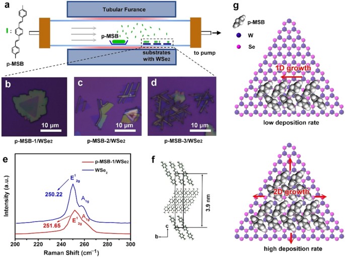
photoelectrical-gating modulation, we develop an electric-gating switchable photodetector based on p-MSB/WSe2. RESULTS EPITAXIAL GROWTH OF 2D VAN-DER-WAALS P-MSB/WSE2 INTERFACE Triangle 2D
WSe2 crystals were produced on SiO2 (300 nm)/Si substrates by chemical vapor deposition (CVD), and then epitaxial growth of p-MSB crystals on WSe2 was conducted by PVD at low pressure (Fig.
1a). The p-MSB molecules were evaporated from the center of the tubular furnace and were deposited on three substrates located 12 cm (p-MSB-1/WSe2), 13 cm (p-MSB-2/WSe2), and 14 cm
(p-MSB-3/WSe2) downstream. Figure 1b–d shows optical microscope images of the as-grown samples, which have different morphologies. Most p-MSB-3 crystals have a wire-like structure with
growth direction parallel to the edges of triangle WSe2 crystals. Neighbor wires form an angle of 60°, suggesting the epitaxial growth of p-MSB crystals on the WSe2. Most p-MSB-1 crystals
have a flake-like structure, covering the whole surface of the WSe2. In the p-MSB-2, both morphologies are observed. Figure 1e shows Raman spectra of WSe2 and p-MSB-1/WSe2. The WSe2 has two
characteristic peaks at 250.22 and 257.77 cm−1, corresponding to in-plane (E12g) and out-plane (A1g) vibrational modes, respectively.29 In the case of p-MSB-1/WSe2, these peaks shift to
higher wavelength by 1.43 cm−1 (E12g) and 0.73 cm−1 in (A1g), indicating p-type doping of WSe2 by the p-MSB molecules.30,31 The different shapes of as-grown p-MSB crystal grown on WSe2 are
attributed to the competition between thermodynamic and kinetic factors (Fig. 1f, g).32 At low deposition rate, thermodynamic factor dominates. According to Gibbs–Curie–Wulff theorem, the
equilibrium shape of a crystal minimizes the total surface energy, thus crystals tended to form wire-like shapes as a result of the strong π–π stacking along (100) direction. Higher
concentration of gas-phase molecules is supplied with decreasing the distance. As a result, kinetic factors lead to the extension of every lateral plane regardless of surface free energy
difference, forming large flake crystals on the WSe2. Therefore, sufficient supply of the molecules in PVD results in flake p-MSB crystal/WSe2 heterostructures with large-area high-quality
2D van-der-Waals interface. Atomic force microscope (AFM) image (Supplementary Fig. 1) shows that p-MSB molecules are stacked layer-by-layer with a single-layer thickness of 1.75 nm and a
plane parallel to the WSe2,33 indicating the 2D epitaxial growth mode of p-MSB on the WSe2. The p-MSB-1 crystal has a thickness up to 130 nm after 15 min growth. Thus, it has an adequate
thickness which enables high absorbance of UV light for sensitive photodetection. PHOTOELECTRICAL PROPERTIES OF P-MSB/WSE2 Devices (Fig. 2a, Supplementary Figs. 2–4) were fabricated on
p-MSB-1(130 nm thickness)/WSe2, p-MSB-3/WSe2, pristine WSe2 and pristine p-MSB with Au/Cr electrodes, a p++ Si back gate and 300 nm SiO2 as the gate dielectric by electron beam lithography.
According to the transfer curves (Supplementary Fig. 5), a positive shift of threshold voltage (_V_th) after p-MSB growth on WSe2 indicates p- type doping effect of the p-MSB molecules.30,31
The field effect mobilities are calculated up to 72, 57, and 10−5 cm2/V s for p-MSB-1/WSe2, WSe2, and p-MSB, respectively, indicating high quality of the as-grown samples and the fact that
the charge transport mainly takes place in 2D WSe2 instead of the p-MSB crystal. The devices were exposed under 365 or 405 nm UV light irradiation. The output curves (Fig. 2a, Supplementary
Fig. 6) of p-MSB-1/WSe2 exhibit remarkably increased current (_I__λ_) with light intensity increasing. The photocurrent (_I_ph = _I__λ_ − _I_dark) shows a nearly linear dependence with the
light intensity (Fig. 2b, Supplementary Fig. 7), indicating that there are low density of trap states derived from defects of WSe2 and p-MSB.34,35 Compared with p-MSB-3/WSe2 (Supplementary
Fig. 2), WSe2 (Supplementary Fig. 3) and p-MSB (Supplementary Fig. 4), p-MSB-1/WSe2 has much higher responsivity under the UV light, which can be evaluated by _R_ and _D*_. The _R_ is
calculated by _R_ = _I_ph/_SP_λ,36 where _S_ is the effective area and _P__λ_ is the light intensity. The _D*_ signifies the smallest detectable signal, which is calculated by _D*_ =
_R_(_S_/2e_I_dark)1/2. At a 2 V bias (Fig. 2c, d, Supplementary Fig. 8), _R_ and _D*_ of p-MSB-1/WSe2 are 1135 A/W and 1014 Jones under 365 nm light (10.7 μW/cm2), and 987 A/W and 1013 Jones
under 405 nm light (22.3 μW/cm2), respectively. At a bias of 10 V (Fig. 2e, f), _R_ and _D*_ of p-MSB-1/WSe2 increase to 1.74 × 10⁴ A/W and 1013 Jones under 365 nm light (3.6 μW/cm2), and
3.27 × 10³ A/W and 1013 Jones under 405 nm light (31.6 μW/cm2). Under the same measurement condition, these values are about 1–2 or 3 orders of magnitude higher than that of pristine WSe2 or
p-MSB (Fig. 2c–f), respectively, and are about seven times higher than that of p-MSB-3/WSe2, indicating the importance of the heterostructure and its morphology in achieving high
photodetecting performance. The high _R_ and _D*_ of p-MSB-1/WSe2 are attributed to the photo-gating modulation effect at the heterostructure (Fig. 3a, b). The highest occupied molecular
orbital (HOMO) and lowest unoccupied molecular orbital (LUMO) of p-MSB are 5.6 and 2.7 eV, respectively.37 The valence band maximum (VBM) and conduction band minimum (CBM) of monolayer WSe2
are 5.10 and 3.53 eV, respectively.38 Under illumination, p-MSB serves as a light absorber; most photoexcited carriers are generated in p-MSB due to the strong absorption of UV light
(Supplementary Fig. 9). A built-in electric field across the junction separates the photoexcited electrons and holes. The HOMO of p-MSB is lower than the VBM of WSe2, which allows the
photoexcited holes transfer from p-MSB to WSe2 and then transport in WSe2 under a bias voltage. Owing to the high mobility, the WSe2 serves as the main conduction channel. At the same time,
a 0.83 eV electron-rejected barrier exists between LUMO of p-MSB and CBM of WSe2, thus the photoexcited electrons in WSe2 are trapped at the interface, resulting in unidirectional carrier
injection from p-MSB to WSe2.39 The trapped electrons modulate the conduction of the WSe2, introducing additional increase of photoresponsivity compared with normal photo-gating effect. As a
result of the photo-gating modulation, p-MSB-1/WSe2 has higher _R_ and _D*_ compared with pristine p-MSB and WSe2. The photo-gating effect usually leads to the shift of _V_th under
illumination.4 Fig. 3c shows that the _V_th shifts positively with the increasing incident power from 2 to 573 μW/cm2, which is similar with other photo-gating TMDs-based
photodetectors,4,40,41 proving the photo-gating modulation in p-MSB-1/WSe2. Moreover, the morphology of the interface is of great importance in this process. The high quality and large
interface area of 2D epitaxial p-MSB-1/WSe2 heterostructure prepared by PVD allows efficient charge transfer and trapping in photo-gating modulation, and results in higher photodetecting
performance compared with p-MSB-3/WSe2 (Fig. 2c, d, Supplementary Fig. 2). LARGE PHOTOELECTRIC-GATING EFFECT OF P-MSB/WSE2 The photodetecting performance of p-MSB-1/WSe2 can be further
improved by applying an electric gate (_V_g). The ratio of current at light/dark as a function of gate bias is shown in Supplementary Fig. 10. The transfer curves, _R_ vs. _V_g and _D*_ vs.
_V_g under different incident power density, are shown in Fig. 3c–e, respectively. Under 2 μW/cm2 365 nm light, the _R_ (_V_sd = 2 V) is 1.4 × 10⁵ A/W when _V_g = 0 V, and it increases up to
3.6 × 10⁶ A/W by more than 5 orders when _V_g varies from 20 V to −60 V. This value is 7 orders of magnitude higher than other reported organic-TMDs heterostructures.22,23 _D*_ (_V_sd = 2
V) reaches 2.5 × 10¹⁴ Jones with the incident power density of 2 μW/cm2. The value increases to 8.6 × 10¹⁴ Jones when _V_g varies from 20 V to −60 V. Therefore, compared with the pristine
TMDs or TMDs-based heterostructures (Fig. 3f),42,43 although the _R_ and _D*_ of p-MSB-1/WSe2 are comparable or lower under photo-gating, the values dramatically increase by orders of
magnitude to a level among one of the highest values for TMDs-based heterostructure, to the best of our knowledge, when a negative _V_g is applied. Dramatic increase of photoresponse under a
negative _V_g is attributed to a new type of photo-gating effect, called large photoelectric-gating effect. Unlike normal photo-gating or photoelectric-gating modulation, the p-MSB-1/WSe2
has interfacial energy barrier between LUMO and CBM in band alignment, which allows unidirectional carrier injection. When a negative _V_g is applied, the Femi level of WSe2 shifts
downwards, leading to increase of the interfacial energy barrier. Thus, more and more photoexcited electrons are trapped at the interface, introducing dramatic increase of the photo-gating
modulation. Therefore, as a result of the tunable energy barrier in p-MSB-1/WSe2, the interfacial charge trapping processes are effectively modulated by the synergy of photo-gating and
electric-gating effects, leading to increase of the _R_ and _D*_ by several orders. This mechanism can be proved by the _V_g dependence of the response speed. The dynamic photoresponse of
normalized photocurrent at different _V_g is shown in Fig. 3g. The rise and decay time of photocurrent are 120 and 80 ms when _V_g = 0 V, about 1–2 orders of magnitude faster than that (rise
time: 2 s, decay time: 25 s) when _V_g = −60 V, which indicates that the electrical gating can effectively modulate the charge trapping process, and more electrons are accumulated when a
negative _V_g is applied.44,45 ELECTRIC-GATING SWITCHABLE PHOTODETECTORS As a result of electric-gating modulated charge trapping process (Fig. 4a, b), the photocurrent response of
p-MSB-1/WSe2 can be switched “ON” and “OFF”, or turned up by applying different _V_g. As shown in Fig. 4c, when alternating dark and light illumination (10.7 μW/cm2, 365 nm), the
p-MSB-1/WSe2 photodetector exhibits a good reversible detecting behavior. At _V_g = 0 V, the photocurrent response (at _V_sd = 2 V) remains a low value down to 5.5 nA, corresponding to the
“OFF” state. When applying a negative _V_g, the large photoelectric-gating effect increases the photocurrent response by about 1–3 orders to 200 nA (_V_g = −20 V), 700 nA (_V_g = −40 V), 2.5
μA (_V_g = −60 V), corresponding to the “ON” state. In the “ON” state, the photocurrent response increases with increasing negative _V_g, implying that the photodetector can be turned up by
applying a larger negative _V_g. DISCUSSION In this article, we find that sufficient supply of gas-phase molecules in PVD is pivotal to obtain high-quality 2D epitaxial van-der-Waals
interface of p-MSB/WSe2, which is of great importance for achieving high-performance photodetectors. This finding extends the understanding of controllable growth of organic crystals on
TMDs, and will be valuable for the practical applications of organic/TMDs. More importantly, p-MSB/WSe2 has an electric-gating tunable barrier at the interface, which allows effective
modulation of the interfacial charge trapping process by _V_g. Thus, as a result of the synergy of photo-gating and electric-gating effects, the performance can be dramatically improved by
large photoelectric-gating modulation. At a _V_g of −60 V, _R_ and _D*_ of p-MSB/WSe2 increased to 3.6 × 10⁶ A/W and 8.6 × 10¹⁴ Jones by 25- and 3-folds, which are among the highest values
for TMDs-based heterostructures, orders of magnitude higher than that of van-der-Waals heterostructures without interfacial electric-gating tunable barrier, i.e. graphene/WSe2/graphene (0.1
A/W),26 WSe2/MoS2 p–n junction (0.12 A/W),27 etc. Besides p-MSB/WSe2, this new strategy also has potential for application in heterostructures made of other materials, opening up promising
avenues for designing photodetectors with higher performance. Moreover, we demonstrate an electric-gating switchable photodetector based on the large photoelectric-gating effect, which can
be switched “ON” and “OFF” or be turned up by _V_g, indicating the great potential of this strategy in developing new types of photoelectrical devices or applications. METHODS EPITAXIAL
GROWTH OF P-MSB ON WSE2 Se powder (400 mg, 99.5%, Sigma-Aldrich) and WO3 powder (40 mg, 99.9%, Sigma-Aldrich) were used as precursors for CVD growth of WSe2 crystals. Five milligrams p-MSB
(>98.0%) powder was placed in a quartz boat, locating in the center of the furnace. The p-MSB was purified at 190 oC for 1 h before epitaxial growth. WSe2 crystals were placed downstream
from the p-MSB source. The distance between WSe2 and p-MSB source ranged from 12 to 14 cm. The furnace was heated to 180 °C, and then epitaxial growth took place at a low pressure of 3.1 ×
10−1 Torr (Ar) for 15–25 min. After growth, the furnace was cooled to room temperature in Ar. CHARACTERIZATION The samples were measured by an optical microscope (Olympus), AFM (Multimode 8,
Bruker, noncontact mode), Raman (XploRA, HORIBA JobinYvon, laser: 532 nm), and a ultraviolet and visible spectrophotometer (Lambda 750, Perkin-Elmer). DEVICE FABRICATION AND MEASUREMENT The
drain and source electrodes (5 nm/50 nm Cr/Au) were patterned on the sample by e-beam lithography (FEI, NOVA NANOSEM450) and thermal evaporator (Kurt. J. Lesker, Nano 36). To obtain a
better contact between the sample and the Au/Cr electrodes, the devices were annealed in vacuum at 250 oC for 90 min. Electrical measurements were conducted in ambient using a semiconductor
analyzer (Keysight, B1500A) and a probe station (Everbeing, PE-4). DATA AVAILABILITY Data that support the findings of this study are available from the corresponding authors upon reasonable
request. REFERENCES * Konstantatos, G. et al. Hybrid graphene–quantum dot phototransistors with ultrahigh gain. _Nat. Nanotechnol._ 7, 363–368 (2012). Article Google Scholar * Sun, Z. et
al. Infrared photodetectors based on CVD-grown graphene and pbs quantum dots with ultrahigh responsivity. _Adv. Mater._ 24, 5878 (2012). Article Google Scholar * Hu, C. et al. Synergistic
effect of hybrid PbS quantum dots/2D-WSe2 toward high performance and broadband phototransistors. _Adv. Funct. Mater._ 27, 1603605 (2017). Article Google Scholar * Furchi, M. M.,
Polyushkin, D. K., Pospischil, A. & Mueller, T. Mechanisms of photoconductivity in atomically thin MoS2. _Nano Lett._ 14, 6165–6170 (2014). Article Google Scholar * Lopez-Sanchez, O.,
Lembke, D., Kayci, M., Radenovic, A. & Kis, A. Ultrasensitive photodetectors based on monolayer MoS2. _Nat. Nanotechnol._ 8, 497–501 (2013). Article Google Scholar * Lee, H. S. et al.
MoS2 nanosheet phototransistors with thickness-modulated optical energy gap. _Nano Lett._ 12, 3695–3700 (2012). Article Google Scholar * Choi, W. et al. High-detectivity multilayer MoS2
phototransistors with spectral response from ultraviolet to infrared. _Adv. Mater._ 24, 5832–5836 (2012). Article Google Scholar * Mak, K. F., Lee, C. & Hone, J. A new direct-gap
semiconductor. _Phys. Rev. Lett._ 105, 136805 (2010). Article Google Scholar * Splendiani, A., Sun, L. & Zhang, Y. Emerging photoluminescence in monolayer MoS2. _Nano Lett._ 10,
1271–1275 (2010). Article Google Scholar * Radisavljevic, B. et al. Single-layer MoS2 transistors. _Nat. Nanotechnol._ 6, 147–150 (2011). Article Google Scholar * Wang, H. et al.
Integrated circuits based on bilayer MoS2 transistors. _Nano Lett._ 12, 4674–4680 (2012). Article Google Scholar * Kim, S. et al. High-mobility and low-power thin-film transistors based on
multilayer MoS2 crystals. _Nat. Commun._ 3, 1011 (2012). Article Google Scholar * Nair, R. R. et al. Fine structure constant defines visual transparency of graphene. _Science_ 320,
1308–1308 (2008). Article Google Scholar * Xia, F. et al. Photocurrent imaging and efficient photon detection in a graphene transistor. _Nano Lett._ 9, 1039–1044 (2009). Article Google
Scholar * Britnell, L. et al. Strong light-matter interactions in heterostructures of atomically thin films. _Science_ 340, 1311–1314 (2013). Article Google Scholar * Peng, B., Ang, P. K.
& Loh, K. P. Two-dimensional dichalcogenides for light-harvesting applications. _Nano Today_ 10, 128–137 (2015). Article Google Scholar * Zhang, W. et al. Role of metal contacts in
high-performance phototransistors based on WSe2 monolayers. _ACS Nano_ 8, 8653–8661 (2014). Article Google Scholar * Eda, G. & Maier, S. A. Two-dimensional crystals: managing light for
optoelectronics. _ACS Nano_ 7, 5660–5665 (2013). Article Google Scholar * Kufer, D. et al. Hybrid 2D-0D MoS2-PbS quantum dot photodetectors. _Adv. Mater._ 27, 176–180 (2015). Article
Google Scholar * Dong, H., Zhu, H., Meng, Q., Gong, X. & Hu, W. P. Organic photoresponse materials and devices. _Chem. Soc. Rev._ 41, 1754–1808 (2012). Article Google Scholar * Wang,
C., Dong, H., Hu, W., Liu, Y. & Zhu, D. Semiconducting π-conjugated systems in field-effect transistors: a material Odyssey of organic electronics. _Chem. Rev._ 112, 2208–2267 (2011).
Article Google Scholar * Liu, F. C. et al. Van Der Waals p-n junction based on an organic-inorganic heterostructure. _Adv. Funct. Mater._ 25, 5865–5871 (2015). Article Google Scholar *
He, D. Y. et al. A Van Der Waals p-n heterojunction with organic/inorganic semiconductors. _Appl. Phys. Lett._ 107, 183103 (2015). Article Google Scholar * Liu, X. L. et al. Epitaxial
ultrathin organic crystals on graphene for high-efficiency phototransistors. _Adv. Mater._ 28, 5200–5205 (2016). Article Google Scholar * Jo, S. H. et al. A high-performance WSe2/h-BN
photodetector using a triphenylphosphine (PPh3)-based n-doping technique. _Adv. Mater._ 28, 4824–4831 (2016). Article Google Scholar * Massicotte, M. et al. Picosecond photoresponse in Van
Der Waals heterostructures. _Nat. Nanotechnol._ 11, 42–46 (2016). Article Google Scholar * Lee, C. H. et al. Atomically thin p-n junctions with Van Der Waals heterointerfaces. _Nat.
Nanotechnol._ 9, 676–681 (2014). Article Google Scholar * Bie, Y. Q. et al. A MoTe2-based light-emitting diode and photodetector for silicon photonic integrated circuits. _Nat.
Nanotechnol._ 12, 1124–1129 (2017). Article Google Scholar * Yang, J. et al. Improved growth behavior of atomic-layer-deposited high-k dielectrics on multilayer MoS2 by oxygen plasma
pretreatment. _ACS Appl. Mater. Interfaces_ 5, 4739–4744 (2013). Article Google Scholar * Kang, D. H. et al. High-performance transition metal dichalcogenide photodetectors enhanced by
self-assembled monolayer doping. _Adv. Funct. Mater._ 25, 4219–4227 (2015). Article Google Scholar * Kang, D. H. et al. Controllable nondegenerate p-type doping of tungsten diselenide by
octadecyltrichlorosilane. _ACS Nano_ 9, 1099–1107 (2015). Article Google Scholar * Li, R. J. et al. Gibbs-Curie-Wulff theorem in organic materials: a case study on the relationship between
surface energy and crystal growth. _Adv. Mater._ 28, 1697–1702 (2012). Article Google Scholar * Yang, J. et al. High-quality large-size organic crystals prepared by improved physical
vapor growth technique and their optical gain properties. _J. Phys. Chem. C._ 115, 9171–9175 (2011). Article Google Scholar * Joshi, N. V. _Photoconductivity: Art, Science, and Technology_
(Marcel Dekker, New York, 1990). * Kind, H. et al. Nanowire ultraviolet photodetectors and optical switches. _Adv. Mater._ 14, 158 (2002). Article Google Scholar * Koppens, F. H. L. et
al. Photodetectors based on graphene, other two-dimensional materials and hybrid systems. _Nat. Nanotechnol._ 9, 780–793 (2014). Article Google Scholar * Nakanotani, H. et al.
Blue-light-emitting ambipolar field-effect transistors using an organic single crystal of 1,4-bis (4-methylstyryl) benzene. _Appl. Phys. Express_ 1, 091801 (2008). Article Google Scholar *
Zhou, C. et al. Carrier type control of WSe2 field-effect transistors by thickness modulation and MoO3 layer doping. _Adv. Funct. Mater._ 26, 4223 (2016). Article Google Scholar * Qian,
C. et al. Organic phototransistors: high-performance organic heterojunction phototransistors based on highly ordered copper phthalocyanine/para-sexiphenyl thin films. _Adv. Funct. Mater._
27, 1604933 (2017). Article Google Scholar * Kufer, D. & Konstantatos, G. Highly sensitive, encapsulated MoS2 photodetector with gate controllable gain and speed. _Nano Lett._ 15,
7307–7313 (2015). Article Google Scholar * Octon, T. J. et al. Fast high-responsivity few-layer MoTe2 photodetectors. _Adv. Opt. Mater._ 4, 1750–1754 (2016). Article Google Scholar * Yu,
S. H. et al. Dye-sensitized MoS2 photodetector with enhanced spectral photoresponse. _ACS Nano_ 8, 8285–8291 (2014). Article Google Scholar * Zeng, L. H. et al. High-responsivity UV-vis
photodetector based on transferable WS2 film deposited by magnetron sputtering. _Sci. Rep._ 6, 20343 (2016). Article Google Scholar * Tan, H. et al. Lateral graphene-contacted vertically
stacked WS2/MoS2 hybrid photodetectors with large gain. _Adv. Mater._ 29, 1702917 (2017). Article Google Scholar * Gong, M. et al. Polarity-controlled attachment of cytochrome C for
high‐performance cytochrome C/graphene Van Der Waals heterojunction photodetectors. _Adv. Funct. Mater._ 28, 1704797 (2018). Article Google Scholar Download references ACKNOWLEDGEMENTS
This work was supported by National Program for Thousand Young Talents of China, the National Natural Science Foundation of China (51773041, 21544001, 21603038), Shanghai Committee of
Science and Technology in China (Grant No. 18ZR1404900), State Key Laboratory of Molecular Engineering of Polymers and Fudan University. AUTHOR INFORMATION AUTHORS AND AFFILIATIONS * State
Key Laboratory of Molecular Engineering of Polymers, Department of Macromolecular Science, Fudan University, Shanghai, 200433, China Zhi Cai, Min Cao, Zhepeng Jin, Kongyang Yi, Xiaosong Chen
& Dacheng Wei Authors * Zhi Cai View author publications You can also search for this author inPubMed Google Scholar * Min Cao View author publications You can also search for this
author inPubMed Google Scholar * Zhepeng Jin View author publications You can also search for this author inPubMed Google Scholar * Kongyang Yi View author publications You can also search
for this author inPubMed Google Scholar * Xiaosong Chen View author publications You can also search for this author inPubMed Google Scholar * Dacheng Wei View author publications You can
also search for this author inPubMed Google Scholar CONTRIBUTIONS D.W. designed research and supervised the project. Z.C. prepared the sample and did AFM, Raman, UV measurement. Z.C. and
M.C. did device measurement. J.Z. and Y.Y. prepared the WSe2. X.C. did thermal deposition. D.W. and Z.C. prepared the manuscript. All authors commented on the manuscript. CORRESPONDING
AUTHOR Correspondence to Dacheng Wei. ETHICS DECLARATIONS COMPETING INTERESTS The authors declare no competing interests. ADDITIONAL INFORMATION PUBLISHER'S NOTE: Springer Nature
remains neutral with regard to jurisdictional claims in published maps and institutional affiliations. ELECTRONIC SUPPLEMENTARY MATERIAL SUPPLEMENTARY MATERIAL RIGHTS AND PERMISSIONS OPEN
ACCESS This article is licensed under a Creative Commons Attribution 4.0 International License, which permits use, sharing, adaptation, distribution and reproduction in any medium or format,
as long as you give appropriate credit to the original author(s) and the source, provide a link to the Creative Commons license, and indicate if changes were made. The images or other third
party material in this article are included in the article’s Creative Commons license, unless indicated otherwise in a credit line to the material. If material is not included in the
article’s Creative Commons license and your intended use is not permitted by statutory regulation or exceeds the permitted use, you will need to obtain permission directly from the copyright
holder. To view a copy of this license, visit http://creativecommons.org/licenses/by/4.0/. Reprints and permissions ABOUT THIS ARTICLE CITE THIS ARTICLE Cai, Z., Cao, M., Jin, Z. _et al._
Large photoelectric-gating effect of two-dimensional van-der-Waals organic/tungsten diselenide heterointerface. _npj 2D Mater Appl_ 2, 21 (2018). https://doi.org/10.1038/s41699-018-0066-2
Download citation * Received: 25 February 2018 * Revised: 27 May 2018 * Accepted: 12 June 2018 * Published: 04 July 2018 * DOI: https://doi.org/10.1038/s41699-018-0066-2 SHARE THIS ARTICLE
Anyone you share the following link with will be able to read this content: Get shareable link Sorry, a shareable link is not currently available for this article. Copy to clipboard Provided
by the Springer Nature SharedIt content-sharing initiative