- Select a language for the TTS:
- UK English Female
- UK English Male
- US English Female
- US English Male
- Australian Female
- Australian Male
- Language selected: (auto detect) - EN
Play all audios:
ABSTRACT With the evolving modern-day communication applications, there is a need for an effectively improved performance in multiplication operations. In today’s scenario, multiplication
operations based on Vedic mathematics have the primary advantage that the propagation delay due to a larger number of input bits is reduced compared to other multipliers. Higher speed Vedic
multipliers, especially based on Urdhva Tiryagbhyam (vertically and crosswise) sutra, perform multiplication in a way that allows parallel processing with reduced delay. Compared to
conventional multipliers like array or Booth multipliers, Vedic multipliers may have less area and power, depending on implementation. In this work, a high-speed 64-bit reversible Vedic
multiplier is proposed using five different adders, namely reversible ripple carry adder (RRCA), reversible carry look-ahead adder (RCLA), reversible carry save adder (RCSA), reversible
carry bypass or carry skip adder (RCSKA)adder, and reversible carry select adder (RCSLA). The main objective of utilizing logic optimization in reversible logic along with the Vedic
multiplier is to develop low-power and high-speed digital circuits. The proposed n-bit reversible Vedic multiplier is simulated using Xilinx Vivado 2019.1 and synthesized in the Cadence EDA
tool in 90 nm and 180 nm technology. The proposed 16-bit reversible Vedic multipliers using the proposed 2-bit reversible multiplier provide 24% and 28% less propagation delay than the
related work Mohana Priya et al. (Int. J. Syst. Assur. Eng. Manag. 14:829–835, 2023). The 16-bit reversible Vedic multiplier proposed using the existing 2-bit reversible multiplier provides
53% lesser area and 52% less power than the reference work Deepa et al. (Sadhana 44:197, 2019). Similarly, the proposed 32-bit reversible Vedic multiplier offers 15% better delay than (Padma
et al. in Comput. Electr. Eng. 92:107178, 2021), 53% less area, and 45% less power than (Deepa et al.in Sadhana 44:197, 2019). Using the proposed reversible Vedic multiplier, a 32-bit MAC
unit is designed and implemented using Cadence 90 nm and 180 nm technology. Thus, the proposed work can be applied to the most promising fields such as Microprocessors to design MAC units,
to find the convolution in Digital signal processing applications, Communication, RF sensing applications, etc. SIMILAR CONTENT BEING VIEWED BY OTHERS A MODULAR TECHNIQUE OF BOOTH ENCODING
AND VEDIC MULTIPLIER FOR LOW-AREA AND HIGH-SPEED APPLICATIONS Article Open access 16 December 2023 SYNTHESIS OF A REVERSIBLE QUANTUM VEDIC MULTIPLIER ON IBM QUANTUM COMPUTERS Article Open
access 29 May 2025 DESIGN OF EFFICIENT BINARY MULTIPLIER ARCHITECTURE USING HYBRID COMPRESSOR WITH FPGA IMPLEMENTATION Article Open access 11 April 2024 INTRODUCTION The ancient Indian
Mathematician Sri Bharathi Krishna Tirthaji created a system of mathematics named Vedic mathematics. In the mathematical community, Vedic mathematics is otherwise called as mental
calculation. There is a collection of sixteen different algorithms or Sutras in Vedic mathematics for solving complex mathematical problems1. One of the simple and widely used techniques in
the Vedic multiplication operation is the “Vertically Crosswise” technique, through which more complex problems in multiplication and division operations can be simplified and solved very
quickly in an easy manner to provide reliable and accurate results. There are also thirteen different sub-sutras in Vedic mathematics. The two major steps of any multiplication operation are
partial product generation and the addition of partial products. These two steps can be performed in parallel using Vedic multiplication. Therefore, the processing power gets reduced for
Vedic multiplication since the processor is independent of the clock frequency. The Vedic algorithm provides the major advantage of speed compared to other traditional algorithms. It makes
the Vedic multiplier applicable in high-speed applications. Another major advantage provided by Vedic mathematics is its reliability. The calculations can be made mentally in human minds and
provide accurate results. The algorithms and formulas of Vedic mathematics are easy to understand. The array multiplier is based on add and shift operations. The Booth multiplier is well
known for the signed multiplication operation. The carry save algorithm is used by the Wallace tree multiplier for the improvement of speed. A multiplier based on a Vedic algorithm is simple
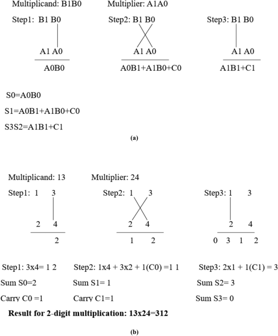
to grasp and is very useful in solving complex multiplication problems. The computation stages of multiplication for a 2-bit Vedic multiplier using the Urdhva algorithm are shown in Fig.
1a. Four sum bits S0, S1, S2, and S3 are generated for a 2-bit Vedic multiplication. Let A1A0 be the multiplier and B1B0 be the multiplicand. The sum bit S0 is obtained by multiplying A0 and
B0 in step 1. The second sum bit S1 is obtained by the multiplication of A0B1 and B0A1 in a vertically crosswise manner. The carry value C0 from the previous stage is added in the second
stage to get the sum bit S1. In step 3, A1 and B1 of the multiplier and multiplicand are multiplied and added with the carry C1 generated from step 2, providing the sum bits S2 and S3. The
Vedic multiplication procedure for 2-digit decimal multiplication is shown in Fig. 1b. In the first step, the LSB digits 3 & 4 are multiplied, and it will provide the result as 12 where
2 is the first sum bit S0 and 1 is considered as carry C0. In the second step, 3 is multiplied by 2, and 4 is multiplied by 1 and then added to the carry from the first step. It will provide
the value 11 where MSB digit 1 is considered as carry C1. In the final step, the MSB bits 2 and 1 are multiplied and added with carry C1, providing the result as 312. REVERSIBLE LOGIC GATES
According to Rolf Landauer, in 1961, energy will be dissipated to the environment when we use conventional irreversible logic gates2. Charles Bennett 1973, implies that the reversible
circuit will have zero power dissipation under ideal circumstances3,4. The power dissipation of the reversible logic circuit is minimal compared to the irreversible circuits. The benefit of
logical reversibility is that the computation can be done in both forward and backward directions. The circuit with reversible logic having an identical number of inputs and outputs is an n
× n circuit5,6,7,8,9,10,11. The design should have a minimum quantum cost. The suitable reversible gates for the proposed circuit design are chosen based on the low quantum cost. During the
generation of the Reversible logic circuits, some garbage outputs may be produced, which is necessary to retrieve the original input information from the output values and maintain the
reversible nature of the circuit. The main motivation for approaching the reversible logic in any circuit design is to obtain lossless computations. SOME PROMINENT REVERSIBLE GATES USED IN
THE REVERSIBLE VEDIC MULTIPLIER DESIGN ARE _BME gate:_ This BME gate has A, B, C, and D as the four input operands and P, Q, R, and S as the four output operands. The quantum cost for this
BME gate is five. The modified BME gate is used along with the modified Peres gate to construct the proposed 2-bit reversible logic multiplier circuit. Figure 2a and b show the reversible
logic BME gate and the modified BME Gate. _HNG gate (Hybrid New Gate):_ The HNG gate uses four inputs, A, B, C, and D. P, Q, R, and S are the four outputs. The quantum cost value for the HNG
gate is six. Instead of full adders, modified designs of Peres gates, HNG gates, CNOT gates, TSG gates, and FRG gates are used to construct the reversible n-bit adder structures to perform
partial product addition operations. The reduction in delay and power value can be obtained for the proposed reversible multiplier structure. Figure 3a and b show the HNG gate and the
modified HNG gate. _Peres gate:_ The Peres gate uses three inputs, A, B, and C. The three outputs of the gate are P, Q, and R. The Peres gate has a quantum cost value of four. Figure 4a and
b show the reversible logic symbol for the Peres and modified Peres gate. The Peres gate can be used for addition, and a combination of modified Peres gates and modified HNG gates can be
used for the addition and ripple carry operations. _CNOT gate (Controlled NOT Gate):_ The other name for the CNOT gate is the Feynman gate. The CNOT gate has A and B as inputs and P and Q as
outputs. The CNOT gate has a quantum cost value of one. Figure 5 shows the symbol for the CNOT gate. The combinations of CNOT and Peres gates are used to design an existing 2-bit reversible
multiplier. The combination of Peres and BME gates is used to construct the proposed reversible multiplier structure. _FRG gate (Fredkin Gate):_ The FRG gate uses A, B, and C as the inputs.
The outputs are P, Q, and R. The other name for the FRG gate is the Fredkin gate. The third input C acts as a controlled input here. When the input C is “1”, the inputs A and B will be
swapped. Otherwise, the inputs go through the circuit unchanged. Hence, the Fredkin gate (FRG) is also called a “Controlled swap gate”. The quantum cost value for the FRG gate is five.
Figure 6a and b show the symbol of the modified FRG gate. Instead of using a conventional multiplexer circuit using basic Boolean logic gates, an FRG gate may act as a multiplexer module for
designing a reversible carry bypass adder circuit. It will further improve the speed of operation. _TSG gate (Thapliyal Srinivas Gate):_ H.Thapliyal and M.B.Srinivas had proposed this TSG
gate, hence the name. The TSG gate is a Propagate Generate Architecture (PGA) gate that uses four inputs, A, B, C, and D. The four outputs are named P, Q, R, and S. The quantum cost for the
TSG gate is four. Figure 7a and b show the symbol of the TSG gate and the modified TSG gate. The TSG gate will do a 3-bit addition operation. Therefore, it can replace the full adder units
in the n-bit reversible adder designs. DIFFERENCE BETWEEN IRREVERSIBLE CONVENTIONAL LOGIC EX-OR GATE AND REVERSIBLE LOGIC EX-OR GATE (FEYNMAN GATE OR CONTROLLED NOT GATE) FOR BETTER
UNDERSTANDING The irreversible logic ex-or operation displayed in Table 1 shows that the output value for C will be logic ‘0’ for both the input combinations (00,11) of the inputs A and B.
Similarly, the output value for C will be logic ‘1’ for the input combinations (01,10). Thus, the input information is impossible to trace using the irreversible conventional logic gates.
Every output combination of reversible ex-or logic shown in Table 2 has a unique input combination. Thus, reversible logic gates can trace the input information. Input information loss after
the computation process is neglected by using reversible gates. Even though the unused outputs in the reversible circuits are considered garbage outputs during forward computation, they are
necessary for retrieving the input values from the output values during the backward computation process. MATERIALS AND METHODS REVERSIBLE ADDER DESIGN The digital logic circuit performs
arithmetic operations, especially addition operations is the adder. The adder is the fundamental component of any computer architecture. Adders are used to perform mathematical computations
and data processing applications. A digital adder can add the specified input binary numbers and generate sum and carry outputs. Several types of adders exist in digital circuits, like full
adders, half adders, ripple carry adders, carry skip adders, etc. Each adder structure has its advantages, disadvantages, and applications. The simple structure of the adder design is the
half adder design. A reversible Vedic multiplier offers significant advantages in gate delay and circuit design regularity12. The speed and the power consumption of the reversible multiplier
are determined by the type of reversible adders used along with the Urdhva algorithm13. Reversible logic gates of low quantum cost are used to create different adders, resulting in improved
design of the adders. REVERSIBLE RIPPLE CARRY ADDER A combinational circuit used to do the addition of the input operands with sufficient delay is the ripple carry adder. The main advantage
of using the ripple carry adder structure is the simplicity of its design14. The logical expression for full adders in the ripple carry adder structure is represented as follows.
$${\text{Sum}} = {\text{A}} \oplus {\text{B}} \oplus {\text{C}}$$ (1) $${\text{Carry}} = {\text{AB}} + {\text{BC}} + {\text{AC}}$$ (2) where A, B, and C are the single-bit inputs of the full
adders used, and the sum output and carry output are the two single-bit outputs of the full adders. The logical operation of the 4-bit ripple carry adder can be explained as follows. Let
A=1001 and B=1001 be the two 4-bit inputs of the 4-bit ripple carry adder and the carry input is considered zero, then the 4-bit sum output is S=0010 and the carry output is 1. The full
adder stages of the ripple carry adder are replaced with the reversible TSG gates to provide better performance with low power dissipation. One Peres gate and a series of three reversible
logic TSG gates are used to design a 4-bit Reversible ripple carry adder. Figure 8 shows the block diagram representation of the ripple carry adder using reversible logic gates. REVERSIBLE
CARRY-LOOKAHEAD ADDER In arithmetic operations like addition and multiplication, propagation delay is a major problem. To overcome the carry propagation delay, the intermediate carry signals
must be generated in advance using the input signals in the carry-lookahead adder. In the carry-lookahead adder design, due to the carry values calculated in advance, there is an
improvement in the speed of the operation with complex hardware structure15,16,17,18,19. The carry look-ahead adder produces two intermediate carry signals, namely carry generate and carry
propagate. The carry propagate value propagates from the first full adder stage to the successive full adders. For Carry generate, the output carry value has to be generated regardless of
the carry input value. The most important terms used in the carry-lookahead adder are carry generate and carry propagate, and they are represented as $${\text{Carry propagate }}\left(
{{\text{Pi}}} \right) = {\text{Ai}} \oplus {\text{Bi}}$$ (3) $${\text{Carry generate }}\left( {{\text{Gi}}} \right) \, = {\text{ Ai}}.{\text{Bi}}$$ (4) The new expressions for the output sum
and the carryout are given by the intermediate carry values calculated using the input signal as follows. $${\text{C1 }} = {\text{ G}}0 \, + {\text{ P}}0{\text{Cin}}$$ (5) $${\text{C2}} =
{\text{G1}} + {\text{P1C1}} = {\text{G1}} + {\text{P1G}}0 + {\text{P1P}}0{\text{C}}0$$ (6) $${\text{C3}} = {\text{G2}} + {\text{P2C2}} = {\text{G2}} + {\text{P2G1}} + {\text{P2P1G}}0 +
{\text{P2P1P}}0{\text{G}}0$$ (7) $${\text{C4}} = {\text{G3}} + {\text{P3C3}} = {\text{G3}} + {\text{P3G2}} + {\text{P3P2G1}} + {\text{P3P2P1G}}0 + {\text{P3P2P1P}}0{\text{G}}0$$ (8) Figure
9a shows the structure of the reversible carry-lookahead adder. Figure 9b represents the block diagram of the intermediate carry value generation. The main advantage of employing the
carry-lookahead adder is that it calculates the intermediate carry values directly using the above-mentioned Eqs. (5), (6), (7) & (8). The input values must be given through the modified
Peres gates to obtain the intermediate carry values based on the equations listed. The major drawback of the carry-lookahead adder is that the carry-generate block becomes highly
complicated for higher-order bits of the carry-lookahead adder. They are implemented as 4-bit modules, and those 4-bit modules are employed in the hierarchical framework to create
higher-order adder structures. REVERSIBLE CARRY SAVE ADDER Carry save adder is a low-cost high-speed adder used for multi-operand addition. The propagation delay time can be reduced by
utilizing this adder. This sort of adder differs from others that saves the carry and adds to the sum value of the next stage full adder instead of transmitting the middle carries to the
next stages20. A conventional carry save adder is a high-speed adder that uses four full adder stages in the upper level of design, producing sum and carry output separately for each full
adder block. In the lower level of design, the full adder stages are connected in series like ripple carry adder to reduce the propagation delay time. Figure 10 shows the structural
representation of the 4-bit reversible carry save adder. The upper level of this adder uses one reversible logic TSG gate and three reversible logic Peres gates. The inputs of the carry save
adder are considered as A=A3A2A1A0, B=B3B2B1B0, and C=0000. Here, the third input is assumed as zero to obtain the addition operation of two 4-bit inputs. The inputs A0, B0, and 0 are the
three inputs given to the first TSG gate, it will produce the sum bit S0 and carry d0. The carry d0 has to be stored and added to the sum t1 produced by the first Peres gate in the upper
level to produce the sum bit S1. The inputs A2, B2, and 0 are given to the third Peres gate in the upper level to produce carry d2. It has to be added with the sum t3 from the final Peres
gate of the upper level. The final sum output of the reversible carry save adder is S3, S2, S1, S0, and the final carry obtained is Cout. The main advantage of this adder is that the carry
can be stored and added to the sum value from the next stage instead of propagating the carry values. Due to the reduced number of carry propagation stages, the computation speed can be
increased. This adder is more suitable for higher-order operations. For lower-order operations, the power consumption will be higher. REVERSIBLE CARRY BYPASS ADDER The carry skip adder or
carry bypass adder optimization challenge is establishing the block sizes and the number of levels required to create the physically fastest carry skip adder. The size and other parameters
of physical devices also affect the addition time. As a result, the design will become more complex. Figure 11a represents the architecture block diagram for the modified reversible carry
bypass adder utilizing modified HNG and FRG gates. In the modified reversible carry bypass adder design, full adders are replaced by four HNG gates, and the FRG gate is used as a 2:1
multiplexer. The select line for the FRG gate acting as a multiplexer in the circuit will be obtained from Fig. 11b. The carry input for the second stage of the HNG gate has to be calculated
look-ahead using a formula and is directly given as a temporary carry TC1. The Peres and CNOT gates are used for the implementation of the modified reversible carry bypass adder select line
circuit. In total, five Peres gates and three CNOT gates are employed to design this adder. Each gate will provide the number of unused garbage outputs depending on the circuit requirement.
The total garbage output obtained for this 4-bit reversible adder is 23. In a conventional carry bypass adder, the carry input has to propagate through each stage of full adders. In the
modified circuit, the carry input TC1 for the second stage of the HNG gate has to be calculated directly using the formula, $${\text{TC1}} = {\text{G}}0 + {\text{P}}0{\text{Cin}}$$ (9) where
G0 is the term “Generate” obtained from the inputs A0 and B0. P0 is the term “Propagate” obtained from the inputs A0 and B0. Cin is the carry input. $${\text{G}}0 = {\text{A}}0\&
{\text{B}}0$$ (10) $${\text{P}}0 = {\text{A}}0 \oplus {\text{B}}0$$ (11) REVERSIBLE CARRY SELECT ADDER If the carry input value is ‘1’, then the structure of the ripple carry adder in the
lower level will operate and provide the sum and the carry output21. Based on the carry input given, the multiplexers present in the circuit will select the final sum bit from the two upper
stages of ripple carry adder structures. The final carry output will be obtained by choosing the carry output from the two stages of the ripple carry adders having the input carry value ‘0’
or ‘1’. Carry select adder design has two stages of the ripple carry adders using full adder units and one stage of 2:1 multiplexer. The first stage uses the input carry value as ‘0’, and
the lower second-stage adder block uses the input carry value as ‘1’. The carry input has to be given to all the stages of the 2:1 multiplexer unit. In the design of the reversible carry
select adder, reversible logic TSG gates replace the full adder, and the 2:1 multiplexer is replaced by the reversible logic FRG gates. The input for this adder design is considered as A0,
A1, A2, A3 and B0, B1, B2, B3. Each stage of the reversible TSG gate will produce its sum bits and carry bits. The FRG gate will determine the final sum bit based on the carry input acting
as the select line. The carry select adder using the reversible logic design is displayed in Fig. 12. REVERSIBLE VEDIC MULTIPLIER DESIGN Reversible gates are used to reduce the information
loss; hence, the power dissipation can be minimized. The design of the Vedic multiplier using the Urdhva algorithm along with the reversible logic results in the reduction of the power
consumption of the circuit, and the speed of the multiplier can be improved22,23. To design the circuit of the reversible multiplier, the modified designs of the Peres gate, BME gate, and
CNOT gates can be used. In the process of partial product addition, HNG gates, TSG gates, and CNOT gates can be used. EXISTING 2-BIT REVERSIBLE VEDIC MULTIPLIER The existing design for a
2-bit reversible Vedic multiplier23 is represented in Fig. 13. It has two input operands, A [1:0] and B [1:0]. The input operand A is given to the pin A and input operand B to the input pin
B of the modified Peres gates. The input pin C of the Peres gate is given with the logic ‘0’. The design of an existing 2-bit reversible multiplier has five Peres Gates and one CNOT gate.
The output is the sum bits Q0, Q1, Q2, and Q3. Thus, a 2-bit multiplier produces a 4-bit sum output. PROPOSED 2-BIT REVERSIBLE VEDIC MULTIPLIER When the gate count, the number of constant
inputs, the number of garbage outputs, and the value of the quantum cost of the circuit get reduced, it is called circuit optimization24,25,26,27. The circuit of the proposed reversible
2-bit Vedic multiplier is represented in Fig. 14. The main objective of logical optimization in design is to obtain the smallest logic circuit with a reduced area cost while maintaining the
same functionality as the original circuit without compromising its simulation efficiency. In the proposed work, the operations performed by a group of gates can be replaced by others that
achieve the same functionality with less space. This process involves reducing the number of components and interconnections, leading to efficient operation and a delay reduction for the
proposed architecture. The proposed design of the reversible multiplier can be used in applications like convolution and cryptography, etc., CAUSES OF REDUCTION IN DELAY OF THE PROPOSED
REVERSIBLE VEDIC MULTIPLIER CIRCUIT * 1. _Reduction in length of the medium:_ The existing design of a 2-bit reversible multiplier uses four wires w1, w2, w3, and w4 to compute the final
result whereas, the proposed design of 2-bit reversible Vedic multiplier uses only three wire connections. When the length of the wire is reduced, the interconnect delay of the circuit is
also reduced. * 2. _Reduction in pin delay:_ The delay of the proposed circuit gets reduced if the pin delay at a transistor gets reduced. * 3. _Logic optimization_: The proposed circuit
attains constraints like reduced chip area and hence the delay can be reduced. PROPOSED 16-BIT REVERSIBLE VEDIC MULTIPLIER The design of a proposed 16-bit multiplier and 8-bit proposed
reversible adder are represented in Fig. 15a and b. This proposed 16-bit reversible Vedic multiplier has two 16-bit input operands and is named A [15:0] and B [15:0]. The output values are
named as S [31:0] and Cout. In the reference work25, the reversible multiplier is designed using the existing 2-bit multiplier architectures, which uses a reversible BVPPG gate, three
reversible Peres gates, and one reversible FG gate. The function call method from the Urdhva algorithm of Vedic mathematics is similar for the higher-order multiplications. This function
call method looks the same as the reference work but uses a different architecture for the proposed work. Two stages of 16-bit reversible adders and one stage of 8-bit reversible adders are
utilized for the addition operations. The modified Peres gate acts like a half adder here, it replaces the OR gate of conventional designs. The final sum output for a 16-bit reversible
multiplier is S [31:0], and one carry output named Cout is obtained from the addition operation performed by reversible adders. The modified designs of Peres and a modified TSG gate are used
to implement the proposed reversible 8-bit adder structure. PROPOSED 32-BIT REVERSIBLE VEDIC MULTIPLIER The design for the 32-bit reversible multiplier is represented in Fig. 16. This
proposed reversible multiplier has two 32-bit input operands, A [31:0] and B [31:0]. The output of this multiplier is named S [63:0] and Cout. Four proposed 16-bit reversible Vedic
multipliers, two stages of 32-bit reversible adder structures, and one stage of 16-bit reversible adder are required to design the proposed 32-bit reversible Vedic multiplier. The
higher-order multipliers and adders are implemented by using the lower-order multipliers and adders. The three stages of reversible adders are employed to obtain the final sum and carry
values. The first stage of the 16-bit reversible multiplier produces the sum bits S [15:0]. The first stage of the 32-bit reversible adder produces its sum and carry output c1. The second
stage of the 32-bit reversible adder will produce its sum bits S [47:16] and carry output c2. A modified Peres gate is used to add the intermediate carry values c1 and c2. The output from
the fourth 16-bit reversible multiplier and the output from the addition operation performed by Peres gate will be given to the final 16-bit adder stage. It employs a combination of Peres
and TSG gates for ripple carry operation. The final 16-bit reversible adder will produce the sum bits S [63:48] and the carry output Cout. PROPOSED 64-BIT REVERSIBLE VEDIC MULTIPLIER The
design for the 64-bit reversible Vedic multiplier is displayed in Fig. 17. The input operands for this proposed reversible logic Vedic multiplier are labeled as A [63:0] and B [63:0]. The
output obtained for this multiplier is labeled as S [127:0] and Cout. The implementation of this proposed 64-bit reversible Vedic multiplier uses four proposed 32-bit reversible Vedic
multipliers and three stages of reversible adder designs. The input operands A [31:0] and B [31:0] are given to the first stage of the 32-bit multiplier. It produces the sum bit as S [31:0].
The input operands A [31:0] and B [63:32] are applied to the second stage of the 32-bit reversible multiplier. A [63:32] and B [31:0] are applied to the third stage of the reversible
multiplier. The two stages of the reversible multiplier in the middle produce its sum bits and will be given as inputs to the first stage of the 64-bit reversible adder. It will generate an
intermediate sum and carry value c1. The second stage of the 64-bit reversible adder produces its sum bits and carry value c2. The carry values c1 and c2 are given to the reversible logic
Peres gate, and the final stage of the 32-bit reversible adder produces the sum bit S [127:96] and carry output Cout. Area, delay, and power reports are obtained for the 64-bit reversible
multiplier built using existing and proposed 2-bit multipliers using five reversible adder structures. The power consumption of the n-bit reversible Vedic multiplier will depend on the type
of adder used. The power consumption of the ripple carry adder will be less, but because of the ripple carry operation, it has more propagation delay. The adder structures need to be
selected based on the requirements of the operation. The performance comparison of the reversible multiplier using five types of adders is represented in Tables 4 and 5. RESULTS AND
DISCUSSION Table 3 represents the comparison of design parameters of the 2-bit existing and proposed reversible Vedic multiplier. The number of reversible gates used to design an existing
2-bit reversible multiplier is 6. The number of garbage outputs produced in this design is 9. The constant inputs used for non-optimized design is 4. The value of the quantum cost of this
multiplier is 21. The summation of gate count value, the number of garbage outputs, the number of constant inputs, and the value of the quantum cost provides the TRLIC value. Hence, the
TRLIC value (Total Reversible Logic Implementation cost) is 40 for the existing 2-bit reversible multiplier. For the proposed 2-bit reversible multiplier, the gate count is reduced to 4. The
proposed design of the 2-bit reversible multiplier uses one BME gate and three Peres gates. The total number of garbage outputs is 7, and the total number of constant inputs required to
obtain the exact operation of the existing multiplier design is 3. The value of the quantum cost of the proposed 2-bit reversible multiplier is 17. Therefore, the TRLIC is reduced to 31 for
the proposed design. The optimized circuit has better design parameter values than the existing circuit designs. The proposed 2-bit multiplier has better design parameter values than the
existing 2-bit reversible multiplier. Table 4 represents the comparison of the design parameters of 4-bit reversible multipliers based on existing and proposed 2-bit reversible Vedic
multipliers using adder structures like the reversible ripple carry adder, reversible carry-lookahead adder, reversible carry save adder, reversible carry bypass adder, and reversible carry
select adder. It shows that the reversible Vedic multiplier designed using the proposed 2-bit multiplier has the lowest gate count and lower value of the garbage outputs than the reversible
Vedic multiplier designed using an existing 2-bit multiplier. The proposed design of a reversible 4-bit multiplier has low TRLIC values. Table 5 compares the existing 4-bit reversible Vedic
multiplier having the ripple carry adder with the proposed one using the ripple carry adder. Ravali et al.24,25,26,27 uses different reversible Vedic multipliers using ripple carry adders
based on reversible logic. On comparing the gate count of all the works mentioned in Table 5, our proposed multiplier design has a lower value. The quantity of the constant inputs is also
small when compared to other works. The value of the quantum cost of the existing design of the multiplier is 128; for the proposed design, the quantum cost value is reduced to 112. The
TRLIC of the24 is 226. For25, the TRLIC is 250. Rakshith et al.26 having the TRLIC value of 274, and for27, the value is 308. The existing multiplier design using a reversible ripple carry
adder has a TRLIC value of 244. For the proposed multiplier, the TRLIC value is only 208. Therefore, the proposed design of the Reversible Vedic multiplier is used for designing higher-order
multipliers such as 16, 32, and 64-bit reversible Vedic multiplier. Based on the design parameters, the perfect adder can be employed in the multiplier design. The reversible adder
structures are implemented in cadence 180 nm technology, and the performance parameters delay, power, and area report are obtained and displayed in Tables 6 and 7. The area and delay
obtained for reversible adders employed in the proposed multiplier are compared to the conventional irreversible adder performance. Conventional adders use full adders and multiplexers to
add the input operands, whereas, in the reversible logic adders design, modified HNG gates and TSG gates are utilized instead of the full adders. A modified FRG gate replaces the multiplexer
circuit in the conventional architecture. The 32-bit and 64-bit reversible adders are implemented, and the delay, area, and power reports are obtained using the cadence tool. The comparison
table shows that the reversible adder offers a reduced delay than the conventional adder designs. Similarly, the area requirement for the reversible adders is minimal compared to the
traditional irreversible adder designs. DELAY, POWER, AND AREA COMPARISON Table 7 shows the comparison of the power report obtained for the reversible adders and the conventional
irreversible adders. The total power report obtained will equal the sum of the leakage power and the Dynamic power. The power consumption of the irreversible ripple carry adder and carry
look-ahead adder is lower. However, the ripple carry adder provides a higher propagation delay. Hence, the speed of the multiplier is reduced by using the ripple carry adder. The reversible
carry look-ahead adder results in high speed of operation with reduced delay and power consumption. The power consumption of the reversible carry save adder, reversible carry select adder,
and reversible carry skip adder is higher due to the hardware complexity. One of the important components employed in the multiplier blocks is the adder structure. The majority of the delay
will be provided by each type of adder used in the design. The speed of the multiplier is decided by the adder employed to add the partial products23,28,29. Hence, the various multipliers
have varying degrees of reduction in delay. The 16, 32, and 64-bit multipliers have been implemented and synthesized using the “Genus synthesis solution tool” of the cadence EDA software
tool in 90nm and 180nm technology. The genus synthesis tool improves the quality of the results. Table 8 shows that the proposed reversible logic Vedic multiplier using reversible adders is
more efficient in delay when compared to the conventional irreversible multiplier. Multipliers having better propagation delay can be suitable for high-speed applications28,29. Table 8 also
shows that the area report obtained for proposed reversible Vedic multipliers is less when compared with the reversible Vedic multipliers based on existing lower order design and
conventional multiplier design using irreversible logic gates. Based on the type of reversible adder utilized, the proposed reversible Vedic multiplier design can be used for high-speed
applications. By employing the pass transistor logic, the power characteristics of the multiplier can further be reduced. Reducing the number of computation steps of the multiplier results
in a high speed of operation30. Modern high-performance applications require fast multipliers for better results31,32,33. The main advantage of the Vedic multiplier is the simultaneous
calculation of the partial product generation and addition34,35,36,37. Table 9 compares the power report obtained for the proposed 16,32, and 64-bit reversible Vedic multiplier to the
existing reversible multiplier and the conventional irreversible multiplier. Because of its simple design and small number of gate counts, the proposed multiplier, which uses a reversible
ripple carry adder consumes less power than other designs. For high-speed operations, we can choose the multiplier with a reversible carry look-ahead adder, and for low-power applications,
reversible multipliers using reversible ripple carry adders can be used. However, the propagation delay is larger for the reversible Vedic multiplier employing the ripple carry adder. Table
10 represents the comparison table for the delay, area, and power report obtained for the proposed 4,8,16, and 32-bit reversible multiplier with the irreversible multiplier of the reference
work38,39,40,41. The comparison has been made between various multiplier circuits implemented using Cadence 90nm and 180nm technology in the ASIC design flow. In38, a high-performance
4,8,16, and 32-bit Vedic multiplier has been designed and synthesized using cadence 90nm and 180nm technology. In the paper39, a 16-bit Vedic signed and unsigned multiplier is created using
the parallel operations of the Urdhava algorithm concept and synthesized using cadence EDA tool utilizing 90 nm technology and cadence Encounter (R)RTL compiler. Mondal et al.40 utilizes
Cadence 45nm technology to design and implement an 8-bit Wallace tree multiplier and Approximate multiplier. For our proposed work, after the behavioral simulation is completed, the
synthesis and implementation have been done using the genus synthesis EDA (Electronics Design Automation) tool that converts a program into a circuit. The standard cell library used in the
proposed work is slow.lib of cadence 90nm and 180nm technology. The standard cell library is a group of low-level electronic logic functions such as AND, OR flip-flops, latches, etc. Then,
the commands syn_gen and syn_map are used to map the design to generic cells and the generic to the 90nm and 180 nm technology. The command syn_opt is used for the post-mapping optimization
process. When compared to38, the proposed work has better area and power values in 180nm technology. When compared to39, the proposed work provides better delay and area values in 180nm
technology. The proposed multiplier performs better and provides smaller delay and power values than the work presented in40. The proposed 32-bit reversible multiplier provides better delay
than the work presented in41 and better area and power values than38. The comparison table indicates that the proposed reversible Vedic multiplier designs have better performance parameters
values when compared to the reference works38,39,40,41. The comparison chart for the delay and power of the 16-bit reversible multiplier employing different adders is displayed in Fig. 18a
and b. Figure 19a and b show the comparison chart for the delay and power of the 32-bit reversible multipliers. Figure 20a and b represent the delay and power comparison of the 64-bit
proposed multiplier design using distinct Adders. The 16,32 & 64-bit reversible Vedic multipliers have been simulated using Xilinx 2019.1 and represented separately in Figs. 21, 22, and
23. The multiplication result of the multipliers using different Adder structures will be the same30,42,43,44,45. In Fig. 21, a 16-bit multiplier has the two input operands of 16-bits a
[15:0], b [15:0], and the sum output will be 32-bit s [31:0] and a carry value 0. Consider the two unsigned decimal inputs of a 16-bit multiplier as 255 and 61680, it will provide the
multiplication result as 15728400. The result indicates the functional accuracy of the multiplication operation39,40,41,46,47,48,49. The simulation waveform for a 32-bit reversible Vedic
multiplier is represented in Fig. 22. The simulation waveform for a 64-bit reversible Vedic multiplier is represented in Fig. 23. The input operands are mentioned as a [63:0], b [63:0], and
the output is mentioned as s [127:0], and cout is the carry output. APPLICATION OF THE PROPOSED REVERSIBLE VEDIC MULTIPLIER A high-speed multiplier plays a crucial role in digital image
processing applications for image smoothening, image sharpening, and refining process of the input image. The proposed Vedic multiplier provides high speed of operation due to the parallel
calculation of the partial product generation and summation of the partial products using the Vedic algorithm. Therefore, the proposed multiplier can be suitable for real-time image
processing applications. The process of Discrete Cosine Transform in image compression algorithm completely relies on the high-speed multiplication operation, and the image segmentation
algorithm also requires efficient multiplication operation. The Vedic multiplier based on the Yuvadunam algorithm can also be used for the square computation, and the Vedic multiplier based
on the Anurupyena algorithm can be employed for the cube computation35. In most modern microprocessor designs, the multiplier is used in the CPU unit to perform the multiplication operation
efficiently. The application of the proposed multiplier in the design of the Arithmetic and Logic Unit of the CPU will provide better overall performance of the multiplier than the
conventional multipliers. A key element used to extract the essential information from the digital signal transmitted through the noisy channel is the digital filter. In digital signal
processing applications, the proposed reversible Vedic multiplier can be employed for designing the FIR and IIR filters due to its higher operating speed. The Vedic multiplication provides
better performance in the cryptography applications like scalar multiplication operation because of its rapid computation. Improved accuracy, security, and scalability of the cryptographic
systems are the results of the application of the Vedic multiplier in the cryptography. 32-BIT MAC UNIT DESIGNED USING THE PROPOSED 32-BIT REVERSIBLE VEDIC MULTIPLIER Using the proposed
32-bit reversible Vedic multiplier, a 32-bit Multiply and Accumulate (MAC) unit has been designed and is shown in Fig. 24. The operation of the MAC unit is one of the most widely used
operations in Digital Signal Processing50. The primary building blocks of the MAC unit are the multiplier block, adder block, and the accumulator unit. In the proposed MAC unit, the basic
multiplier block is replaced by the proposed reversible Vedic multiplier based on the UT algorithm, which provides faster and efficient partial product generation, and the reversible carry
look-ahead adder is used for the addition of the product values from the multiplier and the values stored from the accumulator. The MAC unit receives two inputs: a 32-bit multiplier and a
32-bit multiplicand. The multiplier block generates the product values for the input, and the summation of the product values is carried out by the reversible carry look-ahead adder, which
provides faster operation when compared to the other traditional adders. The output from the adder is then stored in the 65-bit accumulator block. Whenever the clock signal arrives, the
final product of the MAC unit is obtained by adding the value stored in the accumulator to the product value obtained from the multiplier using the reversible carry look-ahead adder. The
performance analysis of the 32-bit MAC unit has been done for the existing irreversible Vedic multiplier along with ripple carry adder and the proposed reversible Vedic multiplier along with
the reversible carry look-ahead adder. PERFORMANCE ANALYSIS OF THE PROPOSED MAC UNIT USING CADENCE GENUS SYNTHESIS TOOL Table 11 shows the performance comparison of the 32-bit MAC unit
designed using the existing irreversible Vedic multiplier and proposed reversible Vedic multiplier in ASIC implementation of 90 nm technology and 180 nm technology. From the analysis part,
it is clearly shown that the MAC unit designed using the proposed 32-bit reversible multiplier provides better delay and power value than the existing works. For microprocessor applications
where a high-speed MAC unit is necessary for the multiplication operations, the proposed multiplier is highly effective and more suitable. The simulation waveform for the proposed 32-bit MAC
unit using the proposed multiplier is shown in Fig. 25. The input of the MAC unit is mentioned as a [31:0] and b [31:0]. The output of the MAC unit is represented as z [64:0]. Whenever the
clock signal goes high, the two input operands are multiplied and added with the product value stored in the accumulator and generate the final output of the MAC unit. CONCLUSIONS In this
work, 4,8,16,32, and 64-bit reversible Vedic multipliers are designed based on the existing 2-bit and proposed 2-bit reversible multipliers using five reversible adder structures. The
proposed reversible Vedic multiplier provides the advantage of a slower rate of delay growth than the irreversible and existing reversible Vedic multipliers. The reversible 4-bit Vedic
multiplier using the proposed 2-bit multiplier has 70% less area and 55% reduced power than38. The proposed reversible Vedic multiplier for 8-bit has 27% less delay than the multiplier
designed in40, 53% lesser area, and 44% reduced power than38. The proposed 16-bit Vedic multiplier provides 28% and 24% less delay than39. The area report obtained for the proposed 16-bit
multiplier is 53% less, and the power report is 52% less than38. The proposed 32-bit multiplier provides 15% less delay than41, 53% less area, and 45% less power value than38. Thus, the
proposed work provides better performance than the existing multipliers. Firstly, a 2-bit reversible Vedic multiplier using one BME gate and three Peres gates is designed and compared to the
2-bit existing reversible multiplier to ensure better design parameters. By utilizing the function call method, 4,8,16,32,64-bit reversible multipliers are designed and simulated using
Xilinx 2019.1. The synthesis has been done using a “genus synthesis solution tool”, namely the EDA (Electronic Design Automation) tool in cadence Virtuoso 90nm and 180nm technology. The
application of the proposed reversible Vedic multipliers is analyzed by implementing a 32-bit MAC unit, and the performance parameters are obtained using Cadence 90m and 180 nm technology
and compared. The comparison results clearly show that the MAC unit designed using the proposed multiplier provides better delay and power values than the MAC unit designed using a
conventional irreversible multiplier in 180nm technology. Thus, the proposed work is highly suitable for high-speed and low-power applications like Microprocessors, Digital signal processing
applications, etc., for high-speed operations. DATA AVAILABILITY All data generated or analyzed during this study are included in this published article. REFERENCES * Jagadguru, S. S. B.,
Krsna,T. Vedic Mathematics or Sixteen Simple Sutras from The Vedas, Motilal Banarsidas, Varanasi (India), (1986). * Landauer, R. Irreversibility and heat generation in the computing process.
_IBM J. Res. Devel._ 5(3), 183–191 (1961). Article MathSciNet MATH Google Scholar * Bennett, C. H. Logical reversibility of computation. _IBM J. Res. Devel._ 17, 525–532 (1973). Article
MathSciNet MATH Google Scholar * Bennett, C. H. Notes on the history of reversible computation. _IBM J. Res. Dev._ 32, 16–23 (1998). Article MathSciNet Google Scholar * Feynman, R.
Quantum mechanical computers. _Optic News_ 11, 11–20 (1985). Article Google Scholar * Frank, M.P. Introduction to Reversible Computing: Motivation, Progress and Challenges, Proceedings of
the 2nd Conference on Computing Frontiers, pp. 385–390, (2005). * Haghparast, M. & Navi, K. A novel fault tolerant reversible gate for nanotechnology based systems. _Am. J. Appl. Sci._
5(5), 519–523 (2008). Article Google Scholar * Ravi, J. N., Vijay Prakash, A. M., Madan, S. Design and Implementation of Digital Components Using Reversible Logic Gates, Int. J. Techn.
Res. Sci. (IJTRS), p. 70, (2017). * Goyal, D. Sharma, V. VHDL implementation of reversible logic gates, Int. J. Adv. Technol. Eng. Res. * Samrin, S. S., Patil, R., Itagi, S., Chetti, S.C.
Tasneem, A. Design of logic gates using reversible gates with reduced quantum cost, Global Trans. Proceedings. (2022). * Gaur, H. & Singh, A. Design of reversible circuits with high
testability. _Electron. Lett._ 52(13), 1102–1104 (2016). Article ADS Google Scholar * Anirudh, A., Prachi, J., Hemavathy, S., Kanchana Bhaaskaran, V. S. Design of Vedic multiplier using
Reversible Logic Gates, In 2020 Second International Conference on Advances in Electrical and Computer Technologies, ICAECT (2020). * Lala, P.K., Parkerson, J.P. Chakraborty, P. Adder
Designs using Reversible logic Gates, WSEAS Trans. Circuits Syst. * Neelam, S., Chitrita, C., Sharad, Y. Reversible adder design for ripple carry and carry look ahead (4, 8, 16, 32-bit),
ICCCA (2016). * Neela, S., Kalyani, P. NageshwarRao, D. Design of a reversible carry look-ahead adder using reversible gates, ISSN No:2348–4845. * Sreekanth, G. Venkata Sudhakar, C. Design
and synthesis of combinational circuits using reversible logic, Int. J. Electron. Electrical Comput. Syst. IJEECS, vol. 7, no. 4 (2018). * Sooriamala, A. P., Thomas, A.K. Korah, R. Study on
reversible logic circuits and analysis, Alliance International Conference on Artificial Intelligence and Machine Learning (AICAAM), (2019). * Morrison, M. Ranganathan, N. A novel
optimization method for reversible logic circuit minimization, In _IEEE Computer Society Annual Symposium on VLSI (ISVLSI)_, pp. 182–187, (2013). * Santosh, R., Amandeep Singh, B. Design and
performance analysis of reversible carry look-ahead adder and carry select adder, ISSN 2229–5518. * Hameed, A.S. Kathem, M.J. High speed modified carry save adder using a structure of
multiplexers, _Int. J. Ele. Com. Eng. (IJECE)_, vol. 11, Iss. 02, pp. 1591–1598, (2020). * Saddam, H. M. & Arifin, F. Design and evaluation of a 32-bit carry select adder using 4-bit
hybrid CLA adder. _AIUB J. Sci. Eng. (AJSE)_ 20(2), 1–7 (2021). Article Google Scholar * Shifana Parween, A. Murugeswari, S. A Design of high speed, area efficient, low power vedic
multiplier using reversible logic gate, Int. J. Emerg. Technol. Adv. Eng. 4(2), (2014). * Sonali, S., Kothule, Shekhar, H., Bodake. High speed, low power vedic multiplier using reversible
logic gate, Int. J. Sci. Res. (IJSR) ISSN (Online): 2319–7064 Index Copernicus Value (2013): 6.14 | Impact Factor, 6.391 (2015). * Ravali, B., Michael Priyanka, M. Ravi, T. Optimized
Reversible logic Design for Vedic Multiplier, In 2015 International Conference on Control, instrumentation, Communication and Computational Technologies(ICCICCT). * Das, A. Kasthuri Bha, J.
K. Design optimization of vedic multiplier using reversible logic, Int. J. Eng. Res. Technol. (IJERT), 3(3), (2014). * Rakshith, S. Rakshith, T. R. Optimized reversible vedic multipliers for
high-speed low power operations, In IEEE Intl. Conf. on Info. &Comm. Tech., (2013). * Haghparast, M., Jafarali Jassbi, S., Navi, K. Hashemipour, O. Design of a novel reversible
multiplier circuit using HNG gate in nanotechnology, World Appl. Sci. J. 3(6), (2008). * Prema, S., Ramanan, S.V., Arun Sekar, R., Rajan, C. High performance reversible vedic multiplier
using cadence 45nm technology, Int. J. Innov. Technol. Exploring Eng. (IJITEE) ISSN: 2278–3075, 8(7), (2019). * Patil Siddhant, V., Pravin, M. VeMSC: Application of vedic mathematics for
designing multipliers, squarers and cubers, Int. J. Eng. Techn. 5(6), (2019). * Padmanabhan, K. K., Seerengasamy, U. & Ponraj, A. S. High-speed grouping and decomposition multiplier for
binary multiplication. _Electronics_ 11, 4202. https://doi.org/10.3390/electronics11244202 (2022). Article Google Scholar * Amjad, H., Ahmad, Z., Abrar, M. & Rasheed, H. Investigation
on performance of single precision floating point multiplier (SPFPM) using CSA multiplier and different types of adders. _Eng. Proc._ 12, 107. https://doi.org/10.3390/engproc2021012107
(2021). Article Google Scholar * Inayat, K. et al. Power-intent systolic array using modified parallel multiplier for machine learning acceleration. _Sensors_ 23, 4297.
https://doi.org/10.3390/s23094297 (2023). Article ADS PubMed PubMed Central Google Scholar * Giustolisi, G. & Palumbo, G. Hybrid full adders: Optimized design, critical review and
comparison in the energy-delay space. _Electronics_ 11, 3220. https://doi.org/10.3390/electronics11193220 (2022). Article Google Scholar * Safoev, N. & Jeon, J.-C. Design and
evaluation of cell interaction based vedic multiplier using quantum-dot cellular automata. _Electronics_ 9(6), 1036. https://doi.org/10.3390/electronics9061036 (2020). Article Google
Scholar * Khubnani, R., Sharma, T. & Subramanyam, C. Applications of vedic multiplier - A review. _Virtual National Conf. Mater. Electron. Appl._
https://doi.org/10.1088/1742-6596/2225/1/012003 (2021). Article Google Scholar * Aizaz, Z. & Khare, K. Energy efficient approximate booth multipliers using compact error compensation
circuit for mitigation of truncation error. _Int. J. Circ. Theor. Appl._ 50(6), 2252–2270. https://doi.org/10.1002/cta.3252 (2022). Article Google Scholar * Aizaz, Z. & Khare, K.
ASMPEC: approximate-sum-based mapping of partial products with error correction for softcore multipliers on FPGAs. _IEEE Trans. Circuits Syst. II Express Briefs_ 70(12), 4569–4573.
https://doi.org/10.1109/TCSII.2023.3292947 (2023). Article Google Scholar * Deepa, A. & Marimuthu, C. N. Design of a high speed Vedic multiplier and square architecture based on
Yuvadunam Sutra. _Sadhana_ 44, 197. https://doi.org/10.1007/s12046-019-1180-3 (2019). Article Google Scholar * Mohana Priya, N., Bennila Thangammal, C., Seshasayanan, R. & Radley, S.
High performance fir filter based on Vedic mathematics. _Int. J. Syst. Assur. Eng. Manag._ 14(3), 829–835. https://doi.org/10.1007/s13198-023-01899-z (2023). Article Google Scholar *
Mondal, S., Marimuthu, R. & Ravi, S. Approximate 8-bit multipliers and their physical design implementation. _e-prime Adv. Electr. Eng. Electron. Energy_ 6, 100300 (2023). Article
Google Scholar * Padma, C., Jagadamba, P. & Ramana, R. P. Design of FFT processor using low power Vedic multiplier for wireless communication. _Comput. Electr. Eng._ 92, 107178 (2021).
Article Google Scholar * Aizaz, Z., Khare, K. & Tirmizi, A. Approximate row-merging-based multipliers for neural network acceleration on FPGAs. _IEEE Embed. Syst. Lett._ 16(2),
126–129. https://doi.org/10.1109/LES.2023.3304678 (2024). Article Google Scholar * Jagadeeswara Rao, E. & Samundiswary, P. Efficient design of modified wallace tree approximate
multipliers based on imprecise compressors for error-tolerance applications. _Arab. J. Sci. Eng._ 49, 4253–4270 (2024). Article Google Scholar * Chinna, V., Gowdar, M.C., Parameshwara,
Design of energy efficient approximate multipliers for image processing applications, Ictact J. Microelectron., 07(01), ISSN: 2395–1680 (Online), https://doi.org/10.21917/ijme.2021.0184.
(2021). * Noorallahzadeh, M., Mosleh, M. & Datta, K. new design of parity-preserving reversible multipliers based on multiple-control toffoli synthesis targeting emerging quantum
circuits. _Front. Comput. Sci._ 18(6), 186908. https://doi.org/10.1007/s11704-023-2492-3 (2024). Article Google Scholar * Kalaiselvi, C. M. & Sabeenian, R. S. Design of area-speed
efficient Anurupyena Vedic multiplier for deep learning applications. _Analog Integr. Circ. Sig. Process_ 119, 521–533. https://doi.org/10.1007/s10470-024-02255-2 (2024). Article ADS
Google Scholar * Shetkar, S. & Koli, S. Area, power efficient Vedic multiplier architecture using novel 4:2 compressor. _Sådhanå_ 48, 216. https://doi.org/10.1007/s12046-023-02274-1
(2023). Article Google Scholar * Jatin, Y., Anupam, K., Shaik, S., Sandeep, B. Navjot, R. Comparative analysis of vedic multiplier using various adder architectures, In 4th International
Conference on Intelligent Circuits and Systems, Journal of Physics: Conference Series 2327, 012022. https://doi.org/10.1088/1742-6596/2327/1/012022. (2022) * Dharani, S., Abin Satheesan,
Asuvanti, M. A., Ranjith, K., Vidhya, S. Design and analysis of high-speed low-power vedic multiplier with 3–1–1–2 compressor using reversible logic gates, In ICMMM 2020, IOP Conf. Series:
Materials Science and Engineering 1059, 012024. https://doi.org/10.1088/1757-899X/1059/1/012024. (2021). * Bharghava Ram Dinesh, K., Vinoth, R. & Kasyap, M. V. R. Design and
Implementation of High Speed 32-bit MAC Unit. _J. Phys. Conf. series_ 2571, 012027. https://doi.org/10.1088/1742-6596/2571/1/012027 (2023). Article Google Scholar Download references
AUTHOR INFORMATION Author notes * Narayanan Mageshwari, Periyasamy Sakthivel and Ramasamy Seetharaman these have equally contributed to this work. AUTHORS AND AFFILIATIONS * Department of
Electronics and Communication Engineering, College of Engineering Guindy Campus, Anna University, Chennai, 600025, India Narayanan Mageshwari, Periyasamy Sakthivel & Ramasamy Seetharaman
Authors * Narayanan Mageshwari View author publications You can also search for this author inPubMed Google Scholar * Periyasamy Sakthivel View author publications You can also search for
this author inPubMed Google Scholar * Ramasamy Seetharaman View author publications You can also search for this author inPubMed Google Scholar CONTRIBUTIONS N.M. and R.S. conceived the
project. N.M. and R.S. carried out the data acquisition, design and analysis. N.M. and R.S. wrote the manuscript. R.S. did the writing of review and editing. P.S. and R.S. did the overall
supervision. All authors equally contributed to this work. All authors reviewed the manuscript. CORRESPONDING AUTHOR Correspondence to Narayanan Mageshwari. ETHICS DECLARATIONS COMPETING
INTEREST The authors declare no competing interests. ADDITIONAL INFORMATION PUBLISHER’S NOTE Springer Nature remains neutral with regard to jurisdictional claims in published maps and
institutional affiliations. RIGHTS AND PERMISSIONS OPEN ACCESS This article is licensed under a Creative Commons Attribution-NonCommercial-NoDerivatives 4.0 International License, which
permits any non-commercial use, sharing, distribution and reproduction in any medium or format, as long as you give appropriate credit to the original author(s) and the source, provide a
link to the Creative Commons licence, and indicate if you modified the licensed material. You do not have permission under this licence to share adapted material derived from this article or
parts of it. The images or other third party material in this article are included in the article’s Creative Commons licence, unless indicated otherwise in a credit line to the material. If
material is not included in the article’s Creative Commons licence and your intended use is not permitted by statutory regulation or exceeds the permitted use, you will need to obtain
permission directly from the copyright holder. To view a copy of this licence, visit http://creativecommons.org/licenses/by-nc-nd/4.0/. Reprints and permissions ABOUT THIS ARTICLE CITE THIS
ARTICLE Mageshwari, N., Sakthivel, P. & Seetharaman, R. Design and synthesis of reversible Vedic multiplier using cadence 180 nm technology for low-power high-speed applications. _Sci
Rep_ 15, 18764 (2025). https://doi.org/10.1038/s41598-025-04002-7 Download citation * Received: 10 January 2025 * Accepted: 23 May 2025 * Published: 28 May 2025 * DOI:
https://doi.org/10.1038/s41598-025-04002-7 SHARE THIS ARTICLE Anyone you share the following link with will be able to read this content: Get shareable link Sorry, a shareable link is not
currently available for this article. Copy to clipboard Provided by the Springer Nature SharedIt content-sharing initiative