- Select a language for the TTS:
- UK English Female
- UK English Male
- US English Female
- US English Male
- Australian Female
- Australian Male
- Language selected: (auto detect) - EN
Play all audios:
ABSTRACT We demonstrate the engineering of waveguide dispersion by lithographically patterning the polymer cladding on silicon nitride waveguide resonators. Both normal and anomalous
dispersion, ranging from − 462 to 409 ps/nm/km, can be achieved for the same waveguide dimension within an integrated photonic chip. In the meantime, this simple process shows no impact on
the waveguide loss and the quality factor of the waveguide resonators, offering flexibility in tailoring designable dispersion for a universal photonic platform. In addition, by adjusting
the coverage ratio of cladding, relatively low dispersion (≈ − 130 ps/nm/km) is also demonstrated in the same waveguide resonator, yielding the potentials for zero-dispersive waveguide
resonators by a proper coverage ratio of the polymer cladding. SIMILAR CONTENT BEING VIEWED BY OTHERS ADAPTED POLING TO BREAK THE NONLINEAR EFFICIENCY LIMIT IN NANOPHOTONIC LITHIUM NIOBATE
WAVEGUIDES Article 26 October 2023 FOURIER SYNTHESIS DISPERSION ENGINEERING OF PHOTONIC CRYSTAL MICRORINGS FOR BROADBAND FREQUENCY COMBS Article Open access 19 June 2023 HYBRID GUIDED
SPACE-TIME OPTICAL MODES IN UNPATTERNED FILMS Article Open access 08 December 2020 The rapid development of silicon photonics provides integrated solutions of miniature, portable, and
mass-productive platforms of chip-based optical functionalities. By confining light propagation in the waveguide core layer, integrated waveguides pave the way for optical applications in
optical communication1, optical sensing2, detection3, signal processing4, and nonlinear optics5. Today, with the aid of the CMOS-compatible fabrication process, large-scale integration
enables the realization of hybrid, compact photonics. Among all of the on-chip devices, the group velocity dispersion (GVD) of optical waveguides is an essential factor in many applications,
such as nonlinear optics, ultrafast optics, and optical communications. Traditionally, the waveguide dispersion can be adjusted with different waveguide geometries and this method has been
widely applied in planar waveguides6,7,8. For instance, normal dispersion can be tuned to anomalous dispersion with a thicker waveguide on the silicon nitride platform7,8. Although the
waveguide geometry can effectively compensate for the material dispersion and offer designable GVD, it loses the flexibility for the waveguide design and trades off the waveguide loss and
available waveguide modes. To alleviate this restriction, several works are aimed at engineering the dispersion by cladding thin films onto waveguides with atomic layer deposition (ALD)9,
sputtering10, or thermal evaporation11. However, this method globally clads the waveguides and defines the dispersion within the entire photonic chip, which is not suitable for engineering
the dispersion of individual devices. To locally define the designable dispersion, several alternatives have been proposed to pattern waveguides with specific structures, such as patterning
oxide cladding with hydrofluoric acid (HF) wet etching12, post-trimmings13, or designing cladding-modulated Bragg gratings14. Nevertheless, these approaches complicate the fabrication
process or the layout design. Additional etching/trimming processes also restrict the available materials for the waveguide core. For example, even with a comparable quality (Q) factor of
lithium niobate (LN) waveguides after patterning oxide cladding12, HF wet etching may easily damage Si3N415 or GaAs waveguides16. A recent work proposed the capability to flexibly adjust
waveguide dispersion using SU-8 polymer as the cladding layer17. The patternable feature of the polymer cladding enables the waveguide dispersion to be engineered in a reconstructable
manner. In this work, we demonstrate waveguide engineering with the polymer cladding layer on Si3N4 waveguide resonators. In comparison to the previous findings, our works result in several
new achievements. First, with the SU-8 polymer patterning, the waveguide dispersion can be interpolated to a designable value. We experimentally show the waveguide dispersion with different
coverage ratios at 0%, 25%, 50%, and 100%, revealing that the dispersion values are consistent with those obtained through linear interpolation. Second, for a fully cladding resonator with
lithography patterning, similar intrinsic quality (Q) factors can be achieved in comparing to that without polymer cladding, showing negligible loss from the cladding layer. In the meantime,
the multi-cycle polymer stripping process is demonstrated to validate the reconstructability of dispersion engineering while maintaining negligible impact on waveguide loss. Third, we
successfully realize waveguide dispersion both in normal and anomalous regimes with the same waveguide dimension. Utilizing a thick Si3N4 waveguide, the dispersion can be tailed from
anomalous (409 ps/nm/km) to normal (− 462 ps/nm/km) regime by increasing the coverage ratio of polymer cladding. Last, based on the above demonstrations, a relatively low dispersion ≈ − 130
ps/nm/km can be achieved by reconstructing the cladding with a 50% coverage ratio. It provides the potential to yield a zero-dispersive waveguide with a proper coverage ratio. These findings
are significant for establishing photonic waveguides with varying dispersion values for different applications on the same integrated photonic chip. DEVICE FABRICATION, SIMULATION, AND
OPTICAL MEASUREMENT DEVICE FABRICATION First, a 4 μm thick silicon oxide (SiO2) layer was thermally grown on silicon wafers in a diffusion furnace. Then, we deposited 500 nm/700 nm Si3N4
thin films on wafers with low-pressure chemical vapor deposition (LPCVD), respectively. For the 500-nm thick Si3N4 waveguides, e-beam lithography (EBL) was used to pattern the waveguide
resonators with a negative-tone resist (ma-N 2405). After that, the devices were dry-etched in a high-density plasma etching tool. For the 700-nm thick waveguides, i-line (365 nm) stepper
was used to pattern the waveguide with a positive-tone resist (Sumitomo PFI38). The devices were then dry-etched in a reactive ion etching tool. A focused ion beam (FIB) image of the
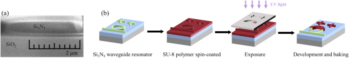
fabricated Si3N4 waveguide with a cross-section 500 nm × 3 μm is shown in Fig. 1a. As for the polymer-cladding layer, the fabrication process is shown in Fig. 1b. SU-8 polymer (GM1040) was
first spin-coated on the air-cladded resonators with a thickness ≈ 1.7 μm. Then, this polymer-cladding layer was patterned by the conventional mask aligner and exposure system. The
fabricated devices with a polymer-cladding layer are shown in Fig. 2. The width of the polymer-cladding layer is 10 μm. To have the SU-8 polymer as part of the final device, a 135 °C hard
bake is performed for 2 h to avoid the surface cracks and increase the cross-linking density18. This process will also help to improve the Q factor of the polymer-cladded resonators.
WAVEGUIDE DISPERSION SIMULATION To verify the capability of dispersion engineering by the polymer cladding, we first explore the dependence of the SU-8 thickness on the dispersion. Figures 3
show the simulated waveguide dispersion with varied SU-8 thicknesses by incorporating both the dispersion curves of SU-8 polymer19 and Si3N4 thin films20. For a Si3N4 waveguide with a
cross-section 500 nm × 3 μm, the waveguide dispersion can be adjusted from − 149 ps/nm-km (without SU-8 polymer) to − 269 ps/nm-km (with a 2 µm SU-8 polymer layer); when considering a
waveguide with a cross-section 700 nm × 3 μm, the dispersion can be fine-tuned from 60 ps/nm-km (without SU-8 polymer) to − 50 ps/nm-km (with a 2 µm SU-8 polymer layer). The dispersion
tuning shows a strong dependence on the varied thickness when the cladding thickness is less than 1 µm. For thicknesses ranging from 1 to 2 µm, the impact becomes less significant as there
is no further overlap observed between the waveguide mode and the relatively thicker SU-8 polymer layer. The corresponding mode profiles with a 2 µm SU-8 polymer layer are shown in the
insets. To adjust the waveguide dispersion by patterning the coverage ratio, a thicker SU-8 layer is preferred to avoid undesired variations caused by the fabrication process of the polymer
spinning. This explains the employment of a 1.7 μm spin-coated SU-8 layer in this study. OPTICAL MEASUREMENT SETUP The measurement setup is shown in Fig. 4. A tunable laser with a tuning
range ≈ 80 nm around 1550 nm was used as the light source for transmission characterization. By coupling light into and out of the Si3N4 waveguides with a pair of lens fibers, the output
signal is then recorded with an oscilloscope. Meanwhile, we use the fiber-based interferometry with 30-m optical path difference to generate interference fringes, providing the calibration
markers of the transmission spectrum. The period of the generated interference fringes is around 6.89 MHz, offering better spectral resolution than that from the tunable laser system. Thus,
this interference spectrum not only calibrates the instability of laser sweeping but also benefits the Q-factor characterization of an ultra-high Q device21. DISPERSION ENGINEERING WITH
POLYMER CLADDINGS DISPERSION INTERPOLATION IN NORMAL DISPERSION VIA DIFFERENT COVERAGE RATIOS OF POLYMER CLADDING For waveguide resonators, the dispersion can be evaluated by the frequency
differences between the adjacent free-spectral-range (FSR) of the cavity. The relation is expressed by the following equation17,22:
$${\varvec{D}}=\frac{{\varvec{c}}}{2{\varvec{\pi}}{{\varvec{\lambda}}}^{2}{\varvec{R}}\cdot
{{\varvec{F}}{\varvec{S}}{\varvec{R}}}^{3}}\frac{{\varvec{d}}{\varvec{F}}{\varvec{S}}{\varvec{R}}}{{\varvec{d}}{\varvec{m}}}$$ (1) where _R_ is the radius of the resonator, _c_ is the speed
of light, _m_ is the azimuthal mode number, _λ_ is the optical wavelength, and \(\frac{dFSR}{dm}\) characterizes the difference between the adjacent FSRs. In this section, we study Si3N4
waveguide resonators with a cross-section 500 nm × 3 μm and a radius 100 μm. Traditionally, this waveguide exhibits normal waveguide dispersion7,8. Figures 5a,b show the measurement results
of air-cladded and polymer-cladded waveguide resonators, respectively, while Fig. 5c is the zoom-in interference spectrum of the fiber-based interferometry. At around 1550 nm wavelength, the
Lorentzian fitting yields the intrinsic quality factor (Qi) ≈ 1.6 × 10⁵ (air-cladding) and ≈ 1.1 × 10⁴ (polymer-cladding without patterning). The corresponding evolution of subsequent FSRs
of the fundamental TE mode is shown in Fig. 5d,e, starting with the FSR located at the lowest sweeping frequency. For the air-cladded waveguide, the difference of the linear-fitted FSR is
7.3 MHz/FSR. As for the one with polymer cladding, the fitted results of FSR difference shift to 14.7 MHz/FSR, showing stronger normal dispersion. The waveguide dispersion is then
interpolated by patterning different coverage ratios of the polymer cladding layer. 25% and 50% coverage ratios are demonstrated by conventional ultraviolet (UV) contact lithography. The
measurement results are shown in Fig. 6. With a 25% coverage ratio, the intrinsic quality factor slightly decreases to Qi ≈ 4.8 × 10⁴ and the fitted FSR difference is 8.9 MHz/FSR. As for the
50% coverage ratio, the intrinsic quality factor Qi ≈ 7.0 × 10⁴ with the fitted FSR difference around 13.0 MHz/FSR. In order to investigate the waveguide dispersion with polymer patterning,
we show the measured dispersion of the resonators with 0%, 25%, 50%, and 100% of coverage ratios within the same chip in Fig. 7. For the air-cladded device with 0% coverage ratio, the
measured dispersion parameter is − 143 ± 26 ps/nm-km, which agrees well with the simulated value − 149 ps/nm-km from the finite element method. As for the 100% polymer-cladded resonator, the
dispersion is − 257 ± 16 ps/nm-km with the simulated value − 267 ps/nm-km. This polymer cladding tailors the dispersion deeper in the normal dispersion regime. When the resonator was
partially polymer-patterned with 25% and 50% coverage ratios, the measured dispersion parameter is then interpolated in between, showing − 175 ± 8 ps/nm-km with the simulated value − 179
ps/nm-km and − 226 ± 14 ps/nm-km with the simulated value − 208 ps/nm-km, respectively, which qualitatively agrees with the simulated waveguide dispersion. This identification suggests that
the dispersion parameter can be flexibly linear-interpolated within a varied dispersion range by patterning the coverage ratio of the polymer cladding layer. FLEXIBLE DISPERSION ENGINEERING
FOR BOTH ANOMALOUS AND NORMAL DISPERSION Next, we demonstrate the engineering for waveguide dispersion from anomalous to normal dispersion within the same device. To realize anomalous
dispersion, waveguide resonators with a cross-section 700 nm × 3 μm and radius 100 μm are used in the air-cladded geometry. By patterning the polymer cladding on resonators, the measurement
results of the fitted dispersion are shown in Fig. 8a, and the corresponding evolution of subsequent FSRs are shown in Fig. 8b–d for 0%, 50%, and 100% coverage ratios, respectively. As
increasing the patterning ratio, the measured waveguide dispersion is then tuned from anomalous (409 ps/nm/km) with air-cladding to normal dispersion (− 462 ps/nm/km) with fully
polymer-cladding; while for the device with 50% coverage ratio, the dispersion is interpolated at ≈ − 130 ps/nm/km. This large tuning range of dispersion provides the potential to realize a
designable waveguide dispersion for different optical functionalities without the need for a specific waveguide dimension or geometry. Besides, by reconstructing the pattering ratio of the
polymer cladding, nearly-zero dispersion could be achieved with a proper coverage ratio. This method provides flexibility to engineer waveguide dispersion for different applications.
DISCUSSION In this section, we further discuss the effect on the waveguide loss and the corresponding Q factors of the waveguide resonators with the polymer cladding. Figure 9 shows the
fitted Q factors from the measurement results of 700 nm × 3 μm resonators. For the air-cladded device, the average intrinsic Q is ≈ 1.0 × 10⁵; while for the 50% and 100% polymer-cladded
devices, the average Qi is 2.5 × 10⁴ and 1.7 × 10⁵, respectively. The slight increasement in the Q factor of the 100% cladded device can be attributed to the better light confinement similar
to that of an oxide-cladded waveguide23. In contrast to the observed degradation of Q factors from 105 to 104 in the spin-coated device without polymer patterning, as mentioned in17, the
demonstrated device is processed by lithographically patterning the polymer around the resonator area. Here, the intrinsic Q factor of the device with 100% coverage remains consistently
greater than 105. In the case of the device with 50% cladding coverage, the degradation of Q factor can be attributed to the discontinuity of the polymer cladding. This leads to scattering
loss in the propagating mode due to the resulting discontinuity of the traveling wave. To address this issue, a polymer taper can be introduced between the regimes with and without the
polymer for mode matching and low-loss conversion, similar to the tapered waveguides previously used in fiber-to-waveguide interconnection24. Moreover, since the fabricated waveguide
resonators support multi-mode propagation, the mode coupling between different mode families results in the abrupt change of Q factors at specific wavelengths25. Next, we study the
susceptibility of the waveguide Q factors with the polymer stripping process. In17, the one-time stripping process demonstrates no impact on the intrinsic Q, highlighting the
reconstructability of dispersion engineering. Here, we further investigate the influence of a multi-cycle SU-8 stripping process on waveguide loss. Figure 10 shows the measured intrinsic Q
of waveguide resonators without the polymer process, with 3-cycle polymer stripping, and with 6-cycle polymer stripping. The stripping process is done by a photoresist remover (PUST-A01).
The intrinsic Qs of the waveguides subjected to multi-cycle polymer stripping remain consistently comparable, indicating a high level of confidence in the reconstructable polymer patterning.
To further emphasize the idea of dispersion engineering by the polymer cladding, another well-known, versatile lithographic resist, polymethyl methacrylate (PMMA) is also used here to
verify the impact on the waveguide Q. This polymer is traditionally used in EBL and its rigid behaviors show stability to both acid and alkaline media26. By spin-coating ≈ 200 nm PMMA on the
Si3N4 waveguide resonators, we show the measured intrinsic Q without and with PMMA cladding in Fig. 11. Again, due to the low absorption of PMMA at telecommunication bands, the intrinsic Qs
are in a similar order after cladding the PMMA polymer. Also, after the PMMA stripping process, the waveguide resonators exhibit similar intrinsic Qs, verifying the reconstructability of
polymer cladding. Last, we compare different schemes of dispersion engineering for Si3N4 integrated waveguides reported previously and summarize in Table 1. Traditionally, by designing the
waveguide geometries, the waveguide dispersion can be well tailored in both normal and anomalous dispersion regimes. However, this scheme loses the flexibility to optimize the waveguide
geometries for better waveguide coupling or loss minimization. Also, it cannot offer different dispersion for each individual device on the same chip unless a complicated fabrication, such
as trimming or etching, is applied12,13. As for the dispersion engineering by cladding with ALD deposition or sputtering, either the tuning range is limited (< 100 ps/nm/km), or precise
control of the cladding thickness is needed. Meanwhile, the dispersion is globally defined within the entire chip when the fabrication process is typically time-consuming. In addition, for
all the previous approaches, the dispersion is not reconstructable. With the polymer cladding, our previous work demonstrates the potential for dispersion reconstructability with patternable
polymer cladding17. Here, we realize the dispersion tailoring in both normal and anomalous dispersion through conventional lithography patterning. Also, for the first time, the waveguide
dispersion of the same waveguide geometry can be flexibly interpolated in between that with and without polymer cladding. SUMMARY In conclusion, we demonstrated the dispersion engineering of
Si3N4 waveguide resonators by patterning polymer cladding with conventional UV-contact lithography. The waveguide dispersion can be tuned from − 462 to 409 ps/nm/km and interpolated both in
normal and anomalous dispersion regimes. Moreover, we showed the potential to obtain relatively low dispersion by patterning a proper coverage ratio of the polymer cladding. Due to the
flexibility of polymer patterning, different waveguide dispersion can be locally assigned to the distinct devices of an integrated photonic chip without deliberately altering the individual
waveguide geometry. This proposed scheme opens up the possibility of compact integrated optical devices for both linear and nonlinear optical functionalities. DATA AVAILABILITY The data used
in this study are available from the corresponding author upon reasonable request. REFERENCES * Jalali, B. & Fathpour, S. Silicon photonics. _J. Lightw. Technol._ 24, 4600–4615 (2006).
Article CAS ADS Google Scholar * Chen, Y., Lin, H., Hu, J. & Li, M. Heterogeneously integrated silicon photonics for the mid-infrared and spectroscopic sensing. _ACS Nano_ 8,
6955–6961 (2014). Article CAS PubMed Google Scholar * Poulton, C. V. _et al._ 2014 Coherent solid-state LIDAR with silicon photonic optical phased arrays. _Opt. Lett._ 42, 4091–4094
(2017). Article CAS PubMed ADS Google Scholar * Perez, D. _et al._ Multipurpose silicon photonics signal processor core. _Nat. Commun._ 8, 636 (2017). Article PubMed PubMed Central
ADS Google Scholar * Leuthold, J., Koos, C. & Freude, W. Nonlinear silicon photonics. _Nat. Photon._ 4, 535–544 (2010). Article CAS ADS Google Scholar * Castelló-Lurbe, D.,
Torres-Company, V. & Silvestre, E. Inverse dispersion engineering in silicon waveguides. _J. Opt. Soc. Am. B_ 31, 1829–1835 (2014). Article ADS Google Scholar * Tan, D. T. H., Ikeda,
K., Sun, P. C. & Fainman, Y. Group velocity dispersion and self phase modulation in silicon nitride waveguides. _Appl. Phys. Lett._ 96, 061101 (2010). Article ADS Google Scholar *
Chavez Boggio, J. M. _et al._ Dispersion engineered silicon nitride waveguides by geometrical and refractive-index optimization. _J. Opt. Soc. Am. B_ 31, 2846–2857 (2014). Article ADS
Google Scholar * Riemensberger, J. _et al._ Dispersion engineering of thick high-Q silicon nitride ring-resonators via atomic layer deposition. _Opt. Express_ 20, 27661–27669 (2012).
Article CAS PubMed ADS Google Scholar * Kiani, K. M. _et al._ Four-wave mixing in high-Q tellurium-oxide-coated silicon nitride microring resonators. _OSA Continuum_ 3, 3497–3507
(2020). Article CAS Google Scholar * Sinobad, M. _et al._ Dispersion trimming for mid-infrared supercontinuum generation in a hybrid chalcogenide/silicon-germanium waveguide. _J. Opt.
Soc. Am. B_ 36, A98–A104 (2019). Article CAS Google Scholar * Wang, C. _et al._ Monolithic lithium niobate photonic circuits for Kerr frequency comb generation and modulation. _Nat.
Commun._ 10, 978 (2019). Article PubMed PubMed Central ADS Google Scholar * Moille, G., Westly, D., Orji, N. G. & Srinivasan, K. Tailoring broadband Kerr soliton microcombs via
post-fabrication tuning of the geometric dispersion. _Appl. Phys. Lett._ 119, 121103 (2021). Article CAS ADS Google Scholar * Sahin, E., Ooi, K. J. A., Png, C. E. & Tan, D. T. H.
Large, scalable dispersion engineering using cladding-modulated Bragg gratings on a silicon chip. _Appl. Phys. Lett._ 110, 161113 (2017). Article ADS Google Scholar * Knotter, D. M. &
Denteneer, T. D. Etching mechanism of silicon nitride in Hf-based solutions. _J. Electrochem. Soc_ 148, F43–F46 (2001). Article CAS Google Scholar * Rei Vilar, M. _et al._
Characterization of wet-etched GaAs (100) surfaces. _Surf. Interface Anal._ 37, 673 (2005). Article CAS Google Scholar * Wang, S.-P., Lee, T.-H., Chen, Y.-Y. & Wang, P.-H. Dispersion
engineering of silicon nitride microresonators via reconstructable SU-8 polymer cladding. _Micromachines_ 13, 454 (2022). Article CAS PubMed PubMed Central Google Scholar * Robin, C.
J., Vishnoi, A. & Jonnalagadda, K. N. Mechanical behavior and anisotropy of spin-coated SU-8 thin films for MEMS. _J. Microelectromech. Syst._ 23, 168–180 (2013). Article Google Scholar
* Datasheet, Microchem SU-8 3000 permanent epoxy negative photoresist (2011). * Luke, K., Okawachi, Y., Lamont, M. R. E., Gaeta, A. L. & Lipson, M. Broadband mid-infrared frequency
comb generation in a Si3N4 microresonator. _Opt. Lett._ 40, 4823–4826 (2015). Article CAS PubMed ADS Google Scholar * Jin, W. _et al._ Hertz-linewidth semiconductor lasers using
CMOS-ready ultra-high-Q microresonators. _Nat. Photon._ 15, 346–353 (2021). Article CAS ADS Google Scholar * Fujii, S. & Takasumi, T. Dispersion engineering and measurement of
whispering gallery mode microresonator for Kerr frequency comb generation. _Nanophotonics_ 9, 1087–1104 (2020). Article Google Scholar * Bogaerts, W. _et al._ Nanophotonic waveguides in
silicon-on-insulator fabricated with CMOS technology. _J. Lightw. Technol._ 23, 401–412 (2005). Article CAS ADS Google Scholar * Wang, P.-H., Liu, H.-C., Chen, H.-Y., Zhong, Y.-X. &
Chen, K. H. CMOS-compatible silicon etched U-grooves with groove-first fabrication for nanophotonic applications. _IEEE Photon. Technol. Lett._ 34, 1230–1233 (2022). Article CAS ADS
Google Scholar * Liu, Y. _et al._ Investigation of mode coupling in normal-dispersion silicon nitride microresonators for Kerr frequency comb generation. _Optica_ 1, 137–144 (2014). Article
CAS ADS Google Scholar * Aziz, S. B., Abdullah, O. G., Hussein, A. M. & Ahmed, H. M. From insulating PMMA polymer to conjugated double bond behavior: Green chemistry as a novel
approach to fabricate small band gap polymers. _Polymers_ 9, 626 (2017). Article PubMed PubMed Central Google Scholar * Okawachi, Y. _et al._ Bandwidth shaping of microresonator-based
frequency combs via dispersion engineering. _Opt. Lett._ 39, 3535–3538 (2014). Article CAS PubMed ADS Google Scholar * Hong, Y., Hong, Y., Hong, J. & Lu, G. W. Dispersion
optimization of silicon nitride waveguides for efficient four-wave mixing. _Photonics_ 5, 161 (2021). Article Google Scholar * Wang, P.-H., Hou, N.-L. & Ho, K.-L. Dispersion
engineering of waveguide microresonators by the design of atomic layer deposition. _Photonics_ 10, 428 (2023). Article CAS Google Scholar Download references ACKNOWLEDGEMENTS The authors
would like to acknowledge chip fabrication support provided by Taiwan Semiconductor Research Institute (TSRI), Taiwan, for i-line lithography, the Nano Facility Center (NFC) of National Yang
Ming Chiao Tung University (NYCU), Taiwan, for LPCVD, oxide diffusion, and FIB processes, and Optical Sciences Center (OSC) of National Central University (NCU), Taiwan, for fabrication
support. P.-H. Wang acknowledges the research financial support from the National Science and Technology Council (NSTC), Taiwan under grant number 111-2221-E-008 -026 and
111-2622-8-008-007-. AUTHOR INFORMATION AUTHORS AND AFFILIATIONS * Department of Optics and Photonics, National Central University, Taoyuan City, 320317, Taiwan Pei-Hsun Wang, Shang-Pu Wang,
Nien-Lin Hou, Zong-Ren Yang, Wei-Hao Huang & Tien-Hsiang Lee Authors * Pei-Hsun Wang View author publications You can also search for this author inPubMed Google Scholar * Shang-Pu Wang
View author publications You can also search for this author inPubMed Google Scholar * Nien-Lin Hou View author publications You can also search for this author inPubMed Google Scholar *
Zong-Ren Yang View author publications You can also search for this author inPubMed Google Scholar * Wei-Hao Huang View author publications You can also search for this author inPubMed
Google Scholar * Tien-Hsiang Lee View author publications You can also search for this author inPubMed Google Scholar CONTRIBUTIONS P.H.W. designed the conception and prepared the
manuscript. S.P.W., W.H.H., and T.H.L. contributed to the device fabrication. S.P.W. and N.L.H. conducted the device characterization. S.P.W., Z.R.Y., N.L.H., and P.H.W. contributed to the
numerical simulations and data analysis. All authors reviewed the manuscript. CORRESPONDING AUTHOR Correspondence to Pei-Hsun Wang. ETHICS DECLARATIONS COMPETING INTERESTS The authors
declare no competing interests. ADDITIONAL INFORMATION PUBLISHER'S NOTE Springer Nature remains neutral with regard to jurisdictional claims in published maps and institutional
affiliations. RIGHTS AND PERMISSIONS OPEN ACCESS This article is licensed under a Creative Commons Attribution 4.0 International License, which permits use, sharing, adaptation, distribution
and reproduction in any medium or format, as long as you give appropriate credit to the original author(s) and the source, provide a link to the Creative Commons licence, and indicate if
changes were made. The images or other third party material in this article are included in the article's Creative Commons licence, unless indicated otherwise in a credit line to the
material. If material is not included in the article's Creative Commons licence and your intended use is not permitted by statutory regulation or exceeds the permitted use, you will
need to obtain permission directly from the copyright holder. To view a copy of this licence, visit http://creativecommons.org/licenses/by/4.0/. Reprints and permissions ABOUT THIS ARTICLE
CITE THIS ARTICLE Wang, PH., Wang, SP., Hou, NL. _et al._ Flexible dispersion engineering using polymer patterning in nanophotonic waveguides. _Sci Rep_ 13, 13211 (2023).
https://doi.org/10.1038/s41598-023-40372-6 Download citation * Received: 30 March 2023 * Accepted: 09 August 2023 * Published: 14 August 2023 * DOI:
https://doi.org/10.1038/s41598-023-40372-6 SHARE THIS ARTICLE Anyone you share the following link with will be able to read this content: Get shareable link Sorry, a shareable link is not
currently available for this article. Copy to clipboard Provided by the Springer Nature SharedIt content-sharing initiative