- Select a language for the TTS:
- UK English Female
- UK English Male
- US English Female
- US English Male
- Australian Female
- Australian Male
- Language selected: (auto detect) - EN
Play all audios:
ABSTRACT Pressure-induced charge density wave (CDW) state can overcome the low-temperature limitation for practical application, thus seeking its traces in experiments is of great
importance. Herein, we provide spectroscopic evidence for the emergence of room temperature CDW order in the narrow pressure range of 10–15 GPa in bulk VSe2. Moreover, we discovered an
8-coordination structure of VSe2 with _C2/m_ symmetry in the pressure range of 35–65 GPa by combining the X-ray absorption spectroscopy, X-ray diffraction experiments, and the
first-principles calculations. These findings are beneficial for furthering our understanding of the charge modulated structure and its behavior under high pressure. SIMILAR CONTENT BEING
VIEWED BY OTHERS LOW-ENERGY ELECTRONIC STRUCTURE IN THE UNCONVENTIONAL CHARGE-ORDERED STATE OF SCV6SN6 Article Open access 12 June 2024 ABERRANT ELECTRONIC AND STRUCTURAL ALTERATIONS IN
PRESSURE TUNED PEROVSKITE NAOSO3 Article Open access 16 September 2020 CHARGE DISPROPORTIONATION AND NANO PHASE SEPARATION IN \(\TEXTIT{R}\MATHRM{SRNIO}_{4}\) Article Open access 22 October
2020 INTRODUCTION Layered 1_T_-VSe2, a typical transition metal dichalcogenide (TMDCs), is an excellent candidate material for the next-generation electronic application and tunable
optoelectronic device1,2,3,4,5. It owns many novel physical properties and exhibits a rich variety of correlated electronic phenomena, such as charge-density-wave (CDW) state6, high-pressure
superconducting7, photoinduced insulator–metal transition8, and possible ferromagnetic order in its monolayer form9,10,11. Among them, the CDW is a low-temperature condensed phase that is
featured by periodic modulation of charge densities accompanied with spontaneous lattice distortion12. It receives much scientific and technological attention and has realized in many
metallic layered TMDCs, such as VX2, NbX2, and TaX2 (where X = Se, Te, etc.)13,14,15,16,17,18. In order to manipulate the CDW order, understanding how it evolves with pressure or substrate
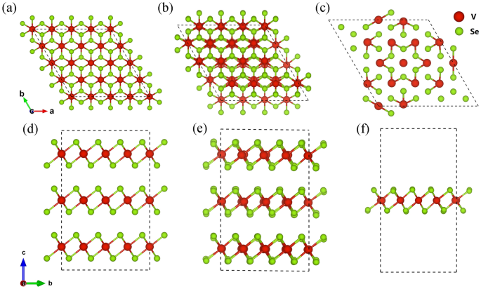
stress is of paramount importance. VSe2 crystallizes in the 1_T_ polytype with a space group of \(P\overline{3}m1{ }\)(CdI2-type structure) at ambient conditions, where the V atoms are
covalently bonded with the octahedra of Se atoms to form a Se-V-Se layer and then these layers are linked through weak van der Waals forces as shown in Fig. 1a,d. 1_T_-VSe2 undergoes an
incommensurate CDW transition around 110 K and commensurate CDW transition around 80 _K_19 driven by the conventional Fermi surface nesting mechanism20 or the newly proposed electron–phonon
coupling21, forming a 4a × 4a × 3c superstructure as shown in Fig. 1b,e. Room-temperature CDW order in bulk VSe2 has recently been observed by Raman spectroscopy under hydrostatic pressure
of 7.4–14.9 GPa22. Pressure-induced _T_CDW enhancement can overcome the limitation of low temperature and offers a promising route for the development of CDW based electronic devices.
Experimental determination of the lattice distortion and structural differences between the normal state and the CDW state is always the priority for any CDW study. Because the distortion or
the atomic displacements in CDW state is extremely small (e.g., 0.1 ~ 0.15 Å in VSe2), the superstructure would only produce relatively weak satellite peaks in the X-ray diffraction
pattern23,24. Thus, seeking the traces of pressure-induced CDW by X-ray diffraction or absorption spectroscopy techniques is challenging but highly desired in practice. On the other hand,
reduced dimensionality and interlayer coupling in van der Waals materials gives rise to fundamentally different electronic, magnetism, and multiple charge density orders in monolayers
compared with the bulk9,25. Due to the different preparation conditions, especially the substrate and strain conditions, there are contradictory reports about the magnetism of the VSe2
monolayer. Strong ferromagnetism up to room temperature was reported in monolayer VSe2 on highly oriented pyrolytic graphite and MoS2 substrates9. While some other groups found multiple CDW
orders with paramagnetic properties. For instance, Chen et al_._ found a \(\sqrt 7 \times \sqrt 3\) CDW superstructure in 1_T_-VSe2 monolayer/bilayer graphene26. Feng et al_._ discovered an
enhanced \(4 \times 4\) CDW order with the temperature near 140_K_27, in which the so-called Star of David (SoD) unit28 can be formed in the center as shown in Fig. 1c,f. In addition, 2
\(\times \;\sqrt 3\) and 4 \(\times \;\sqrt 3\) CDW orders with a transition temperature of 350 and 100 K have also been reported29,30. A combined study of scanning tunneling microscopy and
angle-resolved photoemission spectroscopy clearly demonstrates that the multiple CDW phases in monolayer VSe2, as well as its topography structures, are sensitive to different graphene
substrates and interlayer couplings31,32. The ferromagnetism order is suppressed in those multiple CDW orders, where the underlying substrate or interface may play important roles such as
charge transfer or strain33. At last, tuning the physical properties of the material by applying pressure or by strain requires an understanding of its ground-state crystal structure.
1_T_-VSe2 is stable under ambient condition34. Researchers have achieved great advances in the chemical vapor transport growth of high-quality and large-size 1T-VSe2 single crystals35. Under
high pressure, previous studies mainly focus on the pressure range of 0–30 GPa, and a first-order phase transition has been reported to occur at 15 GPa36. The second phase of VSe2 possess
attractive superconducting properties7, and has been assigned to be the monoclinic NbTe2-type 1_T′_ structure (space group _C2/m_), which are labeled as _C2/m_-I here in order to distinguish
it from another _C2/m_ structure. All reported VSe2 structures consist of six-coordinated V atom. The ground state structure of VSe2 in a higher-pressure range (e.g. 30–65 GPa) or with a
higher V coordination number has not been reported yet. In this work, from the above-mentioned aspects, we systematically studied the bulk VSe2 system using high-pressure X-ray diffraction
(XRD), X-ray absorption fine structure (XAFS) spectroscopy, combining with the first-principles calculations. Herein, we reported two experimental traces of the pressured-induced CDW
transition in bulk VSe2. In addition, we identified an 8 coordination _C2/m_-II structure and established a phase transition pathway of
\(1{\text{T}}\mathop{\longrightarrow}\limits^{{15\;{\text{GPa}}}}\) _C2/m_-\({\text{I}}\mathop{\longrightarrow}\limits^{{35\;{\text{GPa}}}}\) _C2/m_-II (8 coordination) in the pressure range
of 0–65 GPa. METHODS HIGH-PRESSURE XRD MEASUREMENTS Bulk 1T-VSe2 crystals were commercially purchased from 2D semiconductors Inc. and Nanjing 2DNANO Tech. Co., Ltd. In situ high-pressure
XRD experiments were performed at the 4W2 beamline of the Beijing Synchrotron Radiation Facility (BSRF) by angle-dispersive measurements with a wavelength of 0.6199 Å and focused x-ray beam
size of 26 × 8 μm2 (FWHM). Pressure was generated by a symmetric piston-cylinder type diamond anvil cell (DAC) with a pair of diamond anvils with a culet size of 300 μm. A rhenium (Re)
gasket pre-indented to 45 μm in thickness with a drilled hole of 120 μm in diameter was used as the sample chamber. The VSe2 crystals were ground into polycrystalline powder, and then loaded
into the chamber with methanol-ethanol–water (16:3:1) mixture as the pressure-transmitting medium (PTM), which provides quasi-hydrostatic condition up to 11 GPa37 and has been used in
high-pressure XRD experiments for layered materials such as VSe2, TaS2, and BiSe2. No evidence of interaction between VSe2 and methanol: ethanol: water was reported or observed. Two rounds
of experiments were performed. Pressure was determined by the ruby fluorescence technique38. The diffraction patterns were collected by a PILATUS detector and integrated using the FIT2D
software39, and Rietveld refinements on high-pressure data were completed by the GSAS-II package40. HIGH-PRESSURE XAFS MEASUREMENTS The Se _K_-edge XAFS spectra of VSe2 were measured in the
transmission mode at 1W2B beamline of BSRF by a combination of single crystal DAC and polycapillary half-lens to suppress the DAC glitches41. A rhenium (Re) gasket pre-indented to 60 μm
thick with a drilled hole of 120 μm in diameter was used as the sample chamber. Bulk 1_T_-VSe2 crystals were finely grounded and homogeneously mixed with LiF as pressure-transmitting medium
and then loaded into the sample chamber. The edge jump of Se is identified to be around 1 before compression. High-quality, glitch-free XAFS spectra were obtained under non-hydrostatic
pressures up to 53 GPa in the first round of experiment and 63 GPa in the second round of experiment. Pressure was determined by the ruby fluorescence technique. The XANES spectra were
simulated using the FDMNES code42. The extended x-ray absorption fine structure (EXAFS) spectroscopy was background subtracted, normalized, and Fourier transformed (FT) through standard
procedures by ATHENA program. FIRST-PRINCIPLES CALCULATIONS AND CRYSTAL STRUCTURE PREDICTION In order to find a suitable structure to explain the XRD experimental data in the pressure range
of 30–65 GPa, we performed fixed-composition structure prediction using the USPEX code at 30, 50, 70 GPa with 4 and 6 formula units of VSe243,44,45. The searching process was terminated when
the iteration is more than 20 generations with 50 individual structures per generation. Structural relaxations and electronic property calculations were carried out via the generalized
gradient approximation using the Perdew-Burke-Ernzerhof functional (PBE-GGA), as implemented in the Vienna _ab inito_ simulation package (VASP)46,47,48. The projector augmented wave (PAW)
method and plane-wave energy cutoff of 700 eV with a dense k-point grid of spacing 2π × 0.03 Å−1 in the Monkhorst–Pack scheme were used to sample the Brillouin zone and ensure the structural
relaxations with energy and forces converged to less than 10−7 eV and 0.01 eV Å−1, respectively. Grimme DFT-D3 corrections were applied to take van der Waals interactions between the VSe2
layers into consideration. To obtain reasonable pressure-enthalpy curves in Fig. 5, the strongly constrained and appropriately normed (SCAN) meta-generalized gradient approximation
(Meta-GGA) was applied to describe the exchange–correlation potential49. The modulated 3D-CDW state (4a × 4a × 3c superstructure) is obtained from Ref.50 and is fully optimized to its local
minimum on potential energy surface. In order to obtain the 2D structures of various CDW orders in the VSe2 monolayer, we first select a suitable lattice vector to build the superlattices
with an 18 Å vacuum layer introduced to prevent interlayer interaction. Then, a random displacement of all atom in-plane coordinates in the ranges of 1–3% is imposed on the structure25.
Finally, full ionic relaxation of the distorted structure is carried out using the parameter (ISIF = 4) in VASP to obtain the final structures. RESULTS AND DISCUSSION PRESSURE-INDUCED 1T-CDW
TRANSITION IN BULK VSE2 The 1T → CDW transition depends on the relative energy of both structures and the pressure-dependent transition temperature _T_CDW. The enthalpy value of the
nonmagnetic 1_T_-VSe2 (1_T_-NM), ferromagnetic 1_T_-VSe2 (1_T_-FM), and 4a × 4a × 3c CDW superstructure are calculated in the pressure range of 0–20 GPa. As shown in Fig. 2a, the CDW order
is found to be energetically preferred than FM or NM configuration of 1_T_-VSe2, which indicates that it should be the ground state of bulk VSe2 at 0 K, in line with experimental
observations. In addition, the GGA-PBE calculations display that the CDW order is slightly enhanced in the initial 0–4 GPa and then gradually suppressed until vanishing completely due to a
phase transition at 15 GPa. While the FM order in the bulk 1_T_-VSe2 is totally suppressed under compression. The pressure-dependent _T_CDW has been clearly established by the electrical
transport measured22, which is linear enhancement with a constant coefficient. This relationship has been added in Fig. 2a to demonstrating that that the CDW transition approaches
room-temperature at about 10 GPa. Since the _C2/m_ phase appears at 15 GPa, the room-temperature CDW order can only appear in the narrow pressure range of 10–15 GPa. We performed two runs of
high-pressure XRD experiments for 1_T_-VSe2 with special attention to the pressure range of 10–15 GPa. As shown in Fig. 2b, two extra shoulders (labeled by red asterisks) appeared at 13.6 ±
0.4 GPa for the (110) and (011) reflection peaks of the 1_T_ phase. It appears that the new peaks are not caused by the broadening of the 1_T_ diffraction peaks. Moreover, the profile of
the diffraction peak around 22 degree is different from the _C2m_-I phase at 15.5 ± 0.5 GPa. In order to distinguish the three phases, we calculated the theoretical XRD profile of 1_T_, CDW,
and _C2/m_-I structures as shown in Fig. 2d. There are a lot of extra satellite peaks appeared in the theoretical XRD profile, which is in fact not observed in our polycrystalline sample
due to their weak intensity. However, the theoretical profile based on the fully relaxed 3D-CDW superstructure predicts the splitting of two main peaks, which coincides well with the
experimental observations at ~ 14 and ~ 22 degree in Fig. 2b,c. The Rietveld refinements results shown in Figure S1 also support the above hypothesis. Thus, it was considered that the
emergence of the shoulder peaks may be caused by the advent of CDW order. In addition to the lattice information provided by the diffraction pattern, high-pressure XAFS experiments were
performed to monitor the evolution of the local atomic structure and the corresponding electronic state during the transition process in VSe251. Figure 3a,b shows the pressure dependence of
Se _K_-edge EXAFS _k_2χ(_k_) oscillation signals52 and their Fourier transforms (FTs) for VSe2 in the pressure range of 10–17 GPa. The Fourier transforms were characterized by two distinct
peaks: the first peak at around 2.0 Å was ascribed to the nearest neighboring Se-V bond, and the other one at around 2.8 Å was associated with the Se-Se bond. By increasing the pressure, the
V-S coordination peak displayed small variations in the range of 10.81–12.69 and 15.4–17.5GPa, while the Se-Se FT peak was obviously changed due to the _1T_-_C2/m_ phase transition.
Surprisingly, the EXAFS signal of 13.96 ± 0.40 GPa is significantly different from others, especially those in the vicinity of _k_ = 10 Å−1 (marked by a red asterisk in Fig. 3a). The
high-_k_ oscillation signals correspond to a low _R_ peak of the Se-V bond as shown in Fig. 3b. This Se-V shoulder may be associated with the structural distortion that occurred in the
1_T_-CDW transition explained in Fig. 3d, in which the single Se-V bond length is split into multiple bond lengths. This short Se-V bond has not been observed in other pressure ranges and
does not belong to the 1_T_ or _C2/m_-I phases. Moreover, the pressure-dependent absorption edge energy in Fig. 3c follows a power function relationship. It can be observed that there is an
obvious jitter at the 13.96 ± 0.40 GPa for the _E__0_. It deviates from the fitted curve (red dotted line), implying a drastic change of the final state energy, i.e., lowest unoccupied
state, in the dipole transition of 1 s → 4p in Se element. It probably origins from the change in the electron density of the conduction band in the process of CDW formation, which provided
a spectroscopic signature for the metallic 1_T_ phase to the semiconductor-like CDW state. NEW HIGH-PRESSURE PHASE OF BULK VSE2 Combining crystal structure prediction and in situ X-ray
measurements, we identify a new monoclinic VSe2 structure (labeled as _C2/m_-II) in the pressure range of 35–65 GPa. It is generated by the USPEX code and has a similar structure with the
_C2/m_-I phase. The main difference between the two structures is the Wyckoff position of the V atom and the _β_ angle of the lattice. In addition, the coordination number (CN) of the V atom
in _C2/m_-II is 8, while the CN is 6 in 1_T_ and _C2/m_-I phase. Figure 4 shows the pressure-enthalpy curve of various structures in the whole pressure range of 0–60 GPa. The _C2/m_-II
structure was found to have a lower energy than all previously proposed structures in the pressure range of 40–60 GPa. Meanwhile, the phonon dispersion calculations with no imaginary
frequencies further confirmed the dynamical stability53 of the _C2/m_-II phase under 50 and 70 GPa. The pressure-enthalpy curve reveals a complete phase transition pathway of 1_T_ → _C2/m-_I
→ _C2/m-_II and is compatible with the XRD and XAFS experiments. The theoretical phase transition pressure of the 1_T_ → _C2/m_-I is 10 GPa at low temperature, which is smaller than the
actual value of 15 GPa identified by the room-temperature XRD experiments. The 3_R_ phase of VSe2, which is recommended to be the high-pressure phase in the recent report54, was found to be
less stable than the 1_T_ and _C2/m_-I structures in the 0–20 GPa. In addition, we also predicted a non-layered structure of VSe2 with _Pnma_ symmetry, which was added in Fig. 4 for
comparison. The detailed crystal structures and their cell parameters are reported in Table S1 in supplementary materials. Figure 5 shows the selected data of high-pressure XRD experiments
and the Rietveld refinements results based on the 1_T_, _C2m_-I, and _C2/m_-II structures of VSe2. The detailed refined structural parameters are reported in Table S2. The main difference
from the previous experiments is the appearance of the new peak at ~ 15 degree, which first appeared at ~ 37.5 ± 1.1 GPa, gradually enhanced until ~ 60 ± 2 GPa, and finally became stable up
to ~ 67 ± 2 GPa. The experimental observation can be well explained by the 8-coordination monoclinic _C2/m_-II structure. For the pressure range of 32.5–47.6 GPa, VSe2 is probably in a
transition state or a mixed phase of the _C2m_-I and _C2m_-II. The pressure dependence of the unit cell volume and lattice constants are reported in Fig. 6, which is in good agreement with
the theoretical results in Figure S2. The current theoretical and experimental results show that there is volume collapse during the phase transition of _C2m_-I to _C2m_-II. Figure 7 shows
the evolution of the Se _K_-edge XAFS spectra of bulk VSe2. Two runs of experiments were performed with no significant difference found between them, except that the maximum pressure was ~
53 ± 2 GPa for the first round and ~ 63 ± 2 GPa for the second round. The measured spectra at various pressures can be divided into three categories based on the XANES features and EXAFS
signals. The main characteristic of the first phase transition is the splitting of the peak at ~ 3 Å under ~ 17.8 ± 0.5 GPa in Fig. 7b, which indicates the rearrangement of Se atoms in the
second shell. The key characteristic of the second phase transition is the appearance of a new XANES features at ~ 12,676 eV in Fig. 7c. The change of the XAENS features can be well
simulated by the phase transition pathway of 1_T_ → _C2/m-_I → _C2/m-_II shown in Fig. 7d, indicating that it is reasonable to assign the new phase of VSe2 in the pressure range of 35–65 GPa
to be the _C2/m_-II structure. During the second phase transition, the coordination number (CN) of V atoms increased from 6 to 8. The EXAFS fitting shown in Figure S3 clearly supports the
phase transition sequence of 1_T_ → _C2/m-_I → _C2/m-_II. The derived structural parameters are reported in Table S3. The schematic diagram of the whole transition sequence in VSe2 and the
changes in the structure of the vanadium trimers22 are shown in Figure S4. CONCLUSIONS In summary, from first-principles calculations the CDW order is found to be energetically preferred
than FM or NM configuration of 1_T_-VSe2, which indicates that it should be the ground state of bulk VSe2. Based on the high-pressure XRD and XAFS experiments, two experimental anomalies
were detected and attributed to the pressure driven 1_T_ to CDW transition in bulk VSe2. In addition, an eightfold _C_2/m structure was theoretically predicted and experimentally identified
to be a new phase of bulk VSe2 in the pressure range of 35–65 GPa. These findings not only help to determine the ground-state crystal structure of VSe2 but also help to understand the
high-pressure behavior of the charge-ordered state. REFERENCES * Liao, W. _et al._ Interface engineering of two-dimensional transition metal dichalcogenides towards next-generation
electronic devices: recent advances and challenges. _Nanoscale Horiz._ 5, 787–807 (2020). Article ADS CAS PubMed Google Scholar * Zhang, Z. _et al._ Epitaxial growth of two-dimensional
metal-semiconductor transition-metal dichalcogenide vertical stacks (VSe2/MX2) and their band alignments. _ACS Nano_ 13, 885–893 (2019). Article CAS PubMed Google Scholar * Popov, Z. I.
_et al._ The electronic structure and spin states of 2D graphene/VX2 (X = S, Se) heterostructures. _Phys. Chem. Chem. Phys._ 18, 33047 (2016). Article CAS PubMed Google Scholar * Li, J.
_et al._ General synthesis of two-dimensional van der Waals heterostructure arrays. _Nature_ 579, 368–374 (2020). Article ADS CAS PubMed Google Scholar * Zhou, J. _et al._ Large
tunneling magnetoresistance in VSe2/MoS2 magnetic tunnel junction. _ACS Appl. Mater. Interfaces_ 11, 17647–17653 (2019). Article CAS PubMed Google Scholar * Jolie, W. _et al._ Charge
density wave phase of VSe2 revisited. _Phys. Rev. B_ 99, 115417 (2019). Article ADS CAS Google Scholar * Sahoo, S., Dutta, U., Harnagea, L., Sood, A. K. & Karmaker, S.
Pressure-induced suppression of charge density wave and emergence of superconductivity in 1T-VSe2. _Phys. Rev. B_ 101, 014514 (2020). Article ADS CAS Google Scholar * Biswas, D. _et al._
Ultrafast triggering of insulator-metal transition in two-dimensional VSe2. _Nano Lett._ 21, 1968–1975 (2021). Article ADS CAS PubMed Google Scholar * Bonilla, M. _et al._ Strong
room-temperature ferromagnetism in VSe2 monolayers on van der Waals substrates. _Nat. Nanotechnol._ 13, 289–293 (2018). Article ADS CAS PubMed Google Scholar * Boukhvalov, D. W. &
Politano, A. Unveiling the origin of room-temperature ferromagnetism in monolayer VSe2: the role of extrinsic effects. _Nanoscale_ 12, 20875–20882 (2020). Article CAS PubMed Google
Scholar * Xu, K. _et al._ Ultrathin nanosheets of vanadium diselenide: A metallic two-dimensional material with ferromagnetic charge-density-wave behavior. _Angew. Chem. Int. Ed._ 52,
10477–10481 (2013). Article CAS Google Scholar * Pandey, J. & Soni, A. Electron-phonon interactions and two-phonon modes associated with charge density wave in single crystalline
1T-VSe2. _Phys. Rev. Res._ 2, 033118 (2020). Article CAS Google Scholar * Xi, X. _et al._ Strongly enhanced charge-density-wave order in monolayer NbSe2. _Nat. Nanotechnol._ 10, 765–770
(2015). Article ADS CAS PubMed Google Scholar * Yan, J. A., Cruz, M. A. D., Cook, B. & Varga, K. Structural, electronic and vibrational properties of few-layer 2H- and 1T-TaSe2.
_Sci. Rep._ 5, 16646 (2015). Article ADS CAS PubMed PubMed Central Google Scholar * Ngankeu, A. S. _et al._ Quasi-one-dimensional metallic band dispersion in the commensurate charge
density wave of 1T-TaS2. _Phys. Rev. B_ 96, 195147 (2017). Article ADS Google Scholar * Miao, G. _et al._ Real-space investigation of the charge density wave in VTe2 monolayer with broken
rotational and mirror symmetries. _Phys. Rev. B_ 101, 035407 (2020). Article ADS CAS Google Scholar * Wu, Q., Wang, Z., Guo, Y., Yang, F. & Gao, C. Orbital-collaborative charge
density waves in monolayer VTe2. _Phys. Rev. B_ 101, 205105 (2020). Article ADS CAS Google Scholar * Ma, X. _et al._ Charge density wave phase transitions in large-scale few-layer
1T-VTe2 grown by molecular beam epitaxy. _ACS Appl. Mater. Interfaces_ 11, 10729–10735 (2019). Article CAS PubMed Google Scholar * Eaglesham, D. J., Withers, R. L. & Bird, D. M.
Charge-density-wave transitions in 1T-VSe2. _J. Phys. C Solid State Phys._ 19, 359–367 (1986). Article ADS CAS Google Scholar * Sugawara, K. _et al._ Monolayer VTe2: Incommensurate fermi
surface nesting and suppression of charge density waves. _Phys. Rev. B_ 99, 241404 (2019). Article ADS CAS Google Scholar * Diego, J. _et al._ van der Waals driven anharmonic melting of
the 3D charge density wave in VSe2. _Nat. Commun._ 12, 598 (2021). Article ADS CAS PubMed PubMed Central Google Scholar * Feng, J. _et al_. Achieving room-temperature charge density
wave in transition metal dichalcogenide 1T-VSe2. _Adv. Electron. Mater._ 1901427 (2020). * Leroux, M., Cario, L., Bosak, A. & Rodière, P. Traces of charge density waves in NbS2. _Phys.
Rev. B_ 97, 195140 (2018). Article ADS CAS Google Scholar * Lee, J. _et al._ Charge density wave with anomalous temperature dependence in UPt2Si2. _Phys. Rev. B_ 102, 041112 (2020).
Article ADS CAS Google Scholar * Si, J. G. _et al._ Origin of the multiple charge density wave order in 1T-VSe2. _Phys. Rev. B_ 101, 235405 (2020). Article ADS CAS Google Scholar *
Chen, P. _et al._ Unique gap structure and symmetry of the charge density wave in single-layer VSe2. _Phys. Rev. Lett_ 121, 196402 (2018). Article ADS CAS PubMed Google Scholar * Feng,
J. _et al._ Electronic structure and enhanced charge-density wave order of monolayer VSe2. _Nano Lett._ 18, 4493–4499 (2018). Article ADS CAS PubMed Google Scholar * Miller, D. C.,
Mahanti, S. D. & Duxbury, P. M. Charge density wave states in tantalum dichalcogenides. _Phys. Rev. B_ 97, 045133 (2018). Article ADS CAS Google Scholar * Duvjir, G. _et al._
Emergence of a metal-insulator transition and high-temperature charge-density waves in VSe2 at the monolayer limit. _Nano Lett._ 18, 5432–5438 (2018). Article ADS CAS PubMed Google
Scholar * Zhang, D. _et al._ Strain engineering a 4a×√3a charge-density-wave phase in transition-metal dichalcogenide 1T-VSe2. _Phys. Rev. Mater_ 1, 024005 (2017). Article PubMed PubMed
Central Google Scholar * Duvjir, G. _et al._ Multiple charge density wave phases of monolayer VSe2 manifested by graphene substrates. _Nanotechnology_ 32, 364002 (2021). Article Google
Scholar * Park, T. G. _et al._ Interlayer coupling and ultrafast hot electron transfer dynamics in metallic VSe2/graphene van der waals heterostructures. _ACS Nano_ 15, 7756–7764 (2021).
Article CAS PubMed Google Scholar * Rao, R. _et al._ Spectroscopic evaluation of charge-transfer doping and strain in graphene/MoS2 heterostructures. _Phys. Rev. B_ 99, 195401 (2019).
Article ADS CAS Google Scholar * Edla, R. _et al._ Interaction of VSe2 with ambient gases: stability and chemical reactivity. _Phys. Status Solidi RRL_ 2019, 1900332 (2019). Google
Scholar * Feroze, A. _et al._ In-depth structural characterization of 1T-VSe2 single crystals grown by chemical vapor transport. _Cryst. Growth Des._ 20, 2860–2865 (2020). Article CAS
Google Scholar * Sereika, R. _et al._ Novel superstructure-phase two-dimensional material 1T-VSe2 at high pressure. _J. Phys. Chem. Lett._ 11, 380–386 (2020). Article CAS PubMed Google
Scholar * Errandonea, D., Meng, Y., Somayazulu, M. & Hausermann, D. Pressure-induced α→ω transition in titanium metal: a systematic study of the effects of uniaxial stress. _Phys. B
Condensed Matter_ 355, 116–125 (2005). Article ADS CAS Google Scholar * Piermarini, G. J., Block, S., Barnett, J. D. & Forman, R. A. Calibration of the pressure dependence of the R1
ruby fluorescence line to 195 kbar. _J. Appl. Phys._ 46, 2774 (1975). Article ADS CAS Google Scholar * Hammersley, A. P. _et al._ Two-dimensional detector software: from real detector to
idealised image or two-theta scan. _High Press. Res._ 14, 235 (1996). Article ADS Google Scholar * Toby, B. H. EXPGUI, a graphical user interface for GSAS. _J. Appl. Crystallogr._ 34,
210 (2001). Article CAS Google Scholar * Chen, D. L. _et al._ Suppression of Bragg reflection glitches of a single-crystal diamond anvil cell by a polycapillary half-lens in high-pressure
XAFS spectroscopy. _J. Synchrotron Radiat._ 20, 243 (2013). Article CAS PubMed Google Scholar * Joly, Y. X-ray absorption near-edge structure calculations beyond the muffin-tin
approximation. _Phys. Rev. B_ 63, 125120 (2001). Article ADS CAS Google Scholar * Oganov, A. R. & Glass, C. W. Crystal structure prediction using ab initio evolutionary techniques:
Principles and applications. _J. Chem. Phys._ 124, 244704 (2006). Article ADS PubMed CAS Google Scholar * Lyakhov, A. O., Oganov, A. R., Stokes, H. T. & Zhu, Q. New developments in
evolutionary structure prediction algorithm USPEX. _Comput. Phys. Comm._ 184, 1172–1182 (2013). Article ADS CAS Google Scholar * Oganov, A. R., Lyakhov, A. O. & Valle, M. How
evolutionary crystal structure prediction works and why. _Acc. Chem. Res._ 44, 227–237 (2011). Article CAS PubMed Google Scholar * Kresse, G. & Hafner, J. Ab initio molecular
dynamics for liquid metals. _Phys. Rev. B_ 47, 558 (1993). Article ADS CAS Google Scholar * Kresse, G. & Hafner, J. Ab initio molecular-dynamics simulation of the
liquid-metal-amorphous-semiconductor transition in germanium. _Phys. Rev. B_ 49, 14251 (1994). Article ADS CAS Google Scholar * Kresse, G. & Joubert, D. From ultrasoft
pseudopotentials to the projector augmented-wave method. _Phys. Rev. B_ 59, 1758 (1999). Article ADS CAS Google Scholar * Sun, J., Ruzsinszky, A. & Perdew, J. P. Strongly constrained
and appropriately normed semilocal density functional. _Phys. Rev. Lett_ 115, 036402 (2015). Article ADS PubMed CAS Google Scholar * Fumega, A. O. _et al._ Absence of ferromagnetism in
VSe2 caused by its charge density wave phase. _J. Phys. Chem. C_ 123, 27802–27810 (2019). Article CAS Google Scholar * Sun, X. _et al._ In situ unravelling structural modulation across
the charge-density-wave transition in vanadium disulfide. _Phys. Chem. Chem. Phys._ 17, 13333 (2015). Article CAS PubMed Google Scholar * Zhang, W. _et al._ In situ investigation on
doping effect in Co-doped tungsten diselenide nanosheets for hydrogen evolution reaction. _J. Phys. Chem. C_ 125, 6229–6236 (2021). Article CAS Google Scholar * Wu, Y. _et al._
Pressure-induced structural modulations in coesite. _Phys. Rev. B_ 98, 104106 (2018). Article ADS CAS Google Scholar * Pal, S. _et al._ Pressure-induced 1T to 3R structural phase
transition in metallic VSe2: X-ray diffraction and first-principles theory. _Phys. Rev. B_ 104, 014108 (2021). Article ADS CAS Google Scholar Download references ACKNOWLEDGEMENTS This
work was financially supported by the National Natural Science Foundation of China (Grant Nos. 11675206, 11505211 and U1632264) and the National Key Research and Development Program of China
(2017YFA0402800). AUTHOR INFORMATION AUTHORS AND AFFILIATIONS * Beijing Synchrotron Radiation Facility, Institute of High Energy Physics, Chinese Academy of Sciences, Beijing, 100049, China
Zhiying Guo, Xingyu Hao, Juncai Dong, Haijing Li, Jiangwen Liao & Dongliang Chen * University of Chinese Academy of Sciences, Beijing, 100042, China Xingyu Hao, Haijing Li &
Jiangwen Liao Authors * Zhiying Guo View author publications You can also search for this author inPubMed Google Scholar * Xingyu Hao View author publications You can also search for this
author inPubMed Google Scholar * Juncai Dong View author publications You can also search for this author inPubMed Google Scholar * Haijing Li View author publications You can also search
for this author inPubMed Google Scholar * Jiangwen Liao View author publications You can also search for this author inPubMed Google Scholar * Dongliang Chen View author publications You can
also search for this author inPubMed Google Scholar CONTRIBUTIONS D.C. designed the project. H.L. and J.L. did the experiments. J.D. perfomed the DFT calculation. Z. G, and X. H analyzed
the data and wrote the manuscript. All authors reviewed the manuscript. CORRESPONDING AUTHOR Correspondence to Dongliang Chen. ETHICS DECLARATIONS COMPETING INTERESTS The authors declare no
competing interests. ADDITIONAL INFORMATION PUBLISHER'S NOTE Springer Nature remains neutral with regard to jurisdictional claims in published maps and institutional affiliations.
SUPPLEMENTARY INFORMATION SUPPLEMENTARY INFORMATION. RIGHTS AND PERMISSIONS OPEN ACCESS This article is licensed under a Creative Commons Attribution 4.0 International License, which permits
use, sharing, adaptation, distribution and reproduction in any medium or format, as long as you give appropriate credit to the original author(s) and the source, provide a link to the
Creative Commons licence, and indicate if changes were made. The images or other third party material in this article are included in the article's Creative Commons licence, unless
indicated otherwise in a credit line to the material. If material is not included in the article's Creative Commons licence and your intended use is not permitted by statutory
regulation or exceeds the permitted use, you will need to obtain permission directly from the copyright holder. To view a copy of this licence, visit
http://creativecommons.org/licenses/by/4.0/. Reprints and permissions ABOUT THIS ARTICLE CITE THIS ARTICLE Guo, Z., Hao, X., Dong, J. _et al._ Observation of pressure induced charge density
wave order and eightfold structure in bulk VSe2. _Sci Rep_ 11, 18157 (2021). https://doi.org/10.1038/s41598-021-97630-8 Download citation * Received: 25 June 2021 * Accepted: 19 August 2021
* Published: 13 September 2021 * DOI: https://doi.org/10.1038/s41598-021-97630-8 SHARE THIS ARTICLE Anyone you share the following link with will be able to read this content: Get shareable
link Sorry, a shareable link is not currently available for this article. Copy to clipboard Provided by the Springer Nature SharedIt content-sharing initiative