- Select a language for the TTS:
- UK English Female
- UK English Male
- US English Female
- US English Male
- Australian Female
- Australian Male
- Language selected: (auto detect) - EN
Play all audios:
ABSTRACT In current nanoscale semiconductor fabrications, high dielectric materials and ultrathin multilayers have been selected to improve the performance of the devices. Thus, interface
effects between films and the quantification of surface information are becoming key issues for determining the performance of the semiconductor devices. In this paper, we developed an easy,
accurate, and nondestructive diagnosis to investigate the interface effect of hafnium oxide ultrathin films. A roughness scaling method that artificially modified silicon surfaces with a
maximum peak-to-valley roughness range of a few nanometers was introduced to examine the effect on the underlayer roughness. The critical overlayer roughness was be defined by the transition
of RMS roughness which was 0.18 nm for the 3 nm thick hafnium oxide film. Subsequently, for the inline diagnostic application of semiconductor fabrication, the roughness of a mass produced
hafnium film was investigated. Finally, we confirmed that the result was below the threshold set by our critical roughness. The RMS roughness of the mass produced hafnium oxide film was 0.11
nm at a 500 nm field of view. Therefore, we expect that the quantified and standardized critical roughness managements will contribute to improvement of the production yield. SIMILAR
CONTENT BEING VIEWED BY OTHERS HOW LEVELLING AND SCAN LINE CORRECTIONS RUIN ROUGHNESS MEASUREMENT AND HOW TO PREVENT IT Article Open access 17 September 2020 RAPID, NONCONTACT, SENSITIVE,
AND SEMIQUANTITATIVE CHARACTERIZATION OF BUFFERED HYDROGEN-FLUORIDE-TREATED SILICON WAFER SURFACES BY TERAHERTZ EMISSION SPECTROSCOPY Article Open access 25 November 2022 ULTRA-SHALLOW
DOPANT PROFILES AS IN-SITU ELECTRODES IN SCANNING PROBE MICROSCOPY Article Open access 08 March 2022 INTRODUCTION In relation to current industrial semiconductor metrology, the management of
the thickness of ultrathin films has been conducted in a strict manner. Electron microscope studies, such as vertical scanning electron microscopy (VSEM) and transmission electron
microscopy (TEM), are crucial to accurately measuring the thickness of ultrathin films and calibrating optical thickness measurement tools. These instruments are used to measure the films
directly, but practical uses are difficult for inline metrology due to the potential damage to the device during the destructive sampling process1,2,3,4. Ellipsometry is a common approach to
managing the thickness of the transparent and translucent films used in the semiconductor manufacturing process because this method is fast and nondestructive5,6. The film thickness can be
calculated from measuring optical constants, such as the reflection coefficients and phase changes, by detecting the polarized light reflected from the thin film. Although spectral
ellipsometry is a powerful tool when managing film thicknesses at the angstrom (Å) level using a proper micrometer spot size on the illuminated areas, it does not provide sub-nanoscale local
surface information due to the limited lateral resolution associated with this method5,7. Atomic force microscopy (AFM) is an indispensable semiconductor metrology tool that is capable of
reliably and accurately observing surface structures nondestructively8,9,10,11,12,13. It directly assesses the surface morphology and roughness with a sub-nanometer spatial resolution. For
example, the metal etch-back (MEB) depth profiles of dynamic random-access memory (DRAM), for which no signal can be detected by spectroscopic ellipsometry (SE), can be examined by using
inline automated AFM (AAFM). Other examples include: scanning of the channel holes of flash memory devices and the surfaces of solder or copper pillar bump materials, measurements of the
critical dimensions of the mask after development inspection (ADI) processes, and inspections to determine electrical failures in self-aligned contact (SAC) or landing pad (LP) processes in
DRAM modules. In addition, roughness examinations of the ultrathin films without any interference from the lower membrane have been implemented12,14. In recent years, a great deal of
attraction has been paid to improve the performance of the AFM because of the surge of interest in the ultrathin films. Many efforts have been made to replace the gate SiO2 (K = 3.9) layer
with a high dielectric constant (K) to reduce the tunneling current and ensure low power consumption for a complementary metal-oxide semiconductor (CMOS)15,16,17,18,19,20. Among high
dielectric constant materials, hafnium oxide (HfO2) films are being used in the semiconductor industry due to their relatively high K values (K = 25) and large band gaps21. However, the
reliability of HfO2 thin films comes into question on multiple layers due to the poor interfacial quality and inferior thermal stability between the Hf atoms22,23,24,25. Therefore, providing
the criteria pertaining to sub-nanoscale surface roughness has become an important task. We report herein an easy, accurate, and nondestructive diagnosis of the effect on the underlayer
roughness for industrial standard metrology regarding surface roughness. The surface roughness levels of HfO2 thin films were analyzed by a low-noise (LN) AFM system. The surfaces of the
substrates were artificially modified using a wet etching process to examine how the underlayer roughness affects the overlayer roughness, and the relationship between each fabrication step
was investigated. The critical roughness (CR) criterion of the HfO2 thin film can be established according to the intersection between two linear fits. After that, for the inline diagnosis
of semiconductor fabrication, the roughness of a mass produced hafnium film was investigated. We assessed the roughness of a mass-produced HfO2 wafer by using in-line AAFM and LN AFM. From
the results, we confirmed that the roughness of a mass-produced HfO2 wafer with a thickness of 3 nm is below our CR value. The average value of the root mean square (RMS) roughness is 0.11
nm with a 500 nm field of view (FOV), and the dynamic repeatability and reproducibility (R&R) value is 30 pm (the 3 σ value for 10 measurements) for the in-line inspections. Such a
quantified and standardized management of critical roughness by AFM metrology for a few nanometers thin films will help to improve production yield and establish industrial standard
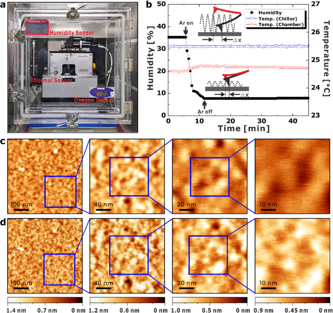
metrology. OPTIMAL ENVIRONMENTAL CONDITIONS FOR ROUGHNESS MEASUREMENTS USING A LOW-NOISE (LN) AFM SYSTEM We constructed a LN AFM system (RMS noise ~35 pm) optimized for surface metrology in
the semiconductor industry and the uncertainty was estimated by a quantitative method (see Supplementary Table 1 in Supplementary Information)26,27,28. The reliability of surface information
is now an essential factor because the results of these measurements can be easily distorted depending on the environment and probe conditions. Low vibration of the tip is necessary for
high-resolution AFM imaging, which is ensured by keeping the distance between the tip and the sample as small as possible. In this experiment, the relative humidity (RH) was held below 10%
by injecting highly pure argon gas, as the measured force can be interrupted by water layers on the substrate29,30,31. The distance between the tip and the sample could be held constant at
4.4 nm. Figure 1 presents the effects of an argon injection on the humidity and shows the differences in the lateral resolution with different field-of-view (FOV) values. At RH 35%,
relatively blurry images were obtained, as shown in Fig. 1c, because the motion of the cantilever is strongly affected by water molecule layers on the sample surface. Conversely, under dry
conditions, the apex of the cantilever can come very close to the sample surface such that clearer images can be taken, as presented in Fig. 1d. For this reason, the RMS roughness in the dry
environment is higher than that in the relatively humid atmosphere. The lateral resolution of the images is high enough to distinguish nanostructures, the grain size of which is less than
10 nm, as shown in Fig. 1d. Ultimately, the LN AFM system was able to visualize the roughness of the HfO2 film at a nanoscale FOV. STUDY OF INTERFACIAL EFFECTS USING THE ROUGHNESS SCALING
METHOD A wet etching process was used to provide a variety of roughness levels of silicon (Si) substrates. The surface roughness was regulated by changing the dipping time in a buffered
oxide etchant (BOE) solution (see Supplementary Fig. 1). In order to examine the spatial resolution by using LN AFM in a range of a few nanometers, the roughness of the Si surface was
increased until the maximum peak-to-valley value (_R__t_) approached 3 nm. This process is designated as the “roughness scaling method” in Fig. 2. The samples that did not undergo the BOE
process are denoted as “0 min” in Fig. 2b,c. An oxygen plasma treatment was conducted after surface etching because the hydrogen-terminated Si surface shows poor nucleation and forms a
nano-island morphology during the atomic layer deposition (ALD) process23,32,33,34,35. An HfO2 layer was deposited onto the surface-treated Si wafers using ALD equipment (Nano-ALD2000; IPS,
Pyeongtaek, Korea) because the insulating film of the mass-produced wafer is a 3 nm thick hafnium oxide film, as shown in Supplementary Fig. 2. Tetrakis (ethylmethylamino) hafnium (TEMAHf)
and ozone (O3) were used to form the hafnium oxide layer at 350 °C. The gas pressure was 0.7 Torr. The surfaces of each of the samples were measured with the LN AFM instrument before and
after the hafnium oxide deposition process. In order to determine the difference between the initial and final states of the surface roughness, the height distributions are overlapped in the
plots, as illustrated in Fig. 3a. The parameters extracted from these distributions, in this case the arithmetic average of the roughness (_R__a_), the RMS roughness (_R__q_), and the
distance between the highest peak and the lowest valley (_R__t_), are listed in Table 1. The RMS roughness and the _R__t_ values are also plotted in Fig. 3b and Supplementary Fig. 3,
respectively. As shown in Fig. 3b and Table 1, the result can be distinguishable into two groups. On the relatively smooth substrates, there is no significant effect on the roughness of the
HfO2 overlayer. It can be explained as the smoothing phenomenon during ALD process that was also observed in other studies25,36. However, the RMS roughness of the HfO2 overlayer is
dramatically increased when the _R__t_ values of the rough silicon surface approaches the thickness of the hafnium oxide film. This phenomenon is significantly related to the conformal
growth of the ALD process since the surface variations are sufficiently high37,38. In other words, the final roughness is less affected by the underlayer (Si substrates) unless the _R__t_
values of the Si substrates match the thickness of the HfO2 film. Thus, we can determine the critical roughness based on the experimental data in Fig. 3b. Two linear fits were conducted to
find each slope and intercept. The parameters of the first linear fit data were calculated by selecting the five lowest data values. The parameters of the second fit data were extracted from
the three highest data values, as shown in Fig. 3b. The critical roughness can be determined from the intersection between the two linear fits, as described by the following equations:
$${{{\rm{CR}}}_{{\rm{over}}}|}_{t=3\,nm}^{Hf{O}_{2}}=\frac{{b}_{1}-\alpha {b}_{2}}{1-\alpha },\,(\alpha \equiv \frac{{a}_{1}}{{a}_{2}})$$ (1) $${{\rm{CR}}}_{{\rm{under}}}=\frac{1}{\beta
}({b}_{1}-{b}_{2}),\,(\beta \equiv {a}_{2}-{a}_{1})$$ (2) where _t_ is the thickness of the hafnium oxide film, _a_1 and _b_1 are correspondingly the slope and the intercept extracted from
the first linear fitting function, and _a_2 and _b_2 are likewise the slope and the intercept of the second linear fitting function. The finally estimated CR value of the HfO2 overlayer in
this dielectric system was 0.18 nm while the CR value of the underlayer was 0.27 nm. Moreover, in order to verify the effectiveness of the CR, we measured the leakage current through the
metal-insulator-metal (MIM) diode structure39,40. As shown in Fig. 3c, the leakage current was rapidly increased after the CR. (see Supplementary Fig. 4 for current density plot of minimum,
median, and maximum data). Therefore, the CR value defined by the simple method in this study proved to be effective. Although the CR value in this experiment is not an absolute criterion
for all hafnium oxide films, we believe that the proposed method will be useful for establishing an industry standard CR. INLINE MORPHOLOGY ANALYSIS OF ULTRATHIN HAFNIUM OXIDE FILMS FOR
INDUSTRIAL METROLOGY During the semiconductor fabrication process, surface morphology measurements of the sub-nanoscale roughness are among the most challenging applications in a typical
facility environment. They require a high performance of the anti-vibration efforts and acoustic shielding while executing atomic force feedback control on the surface. In addition, there
are many items to be considered to obtain reliable data41,42. Thus, we undertook a surface analysis of a mass-produced ultrathin HfO2 film sample (~3 nm in thickness) using an optimized LN
AFM system. Subsequently, roughness measurements of an identical mass-produced HfO2 wafer were conducted using an inline AAFM system (InSight; Bruker Corporation, USA), including an
auto-level stage, automated probe exchange, and thermal stability, the process of which is fully automated for the mass production of these wafers. A highly accurate laser interferometer
stage was used for the measurements. The resonance frequency of the AAFM itself and the fingerprint frequency of the environmental noise in the semiconductor facility were separated to
achieve sub-nanoscale roughness with the in-line AAFM system. The background noise level was approximately 35 pm. The roughness parameters calculated from each topography image are
summarized in Table 2. All roughness parameters are similar except for that in the area with a low FOV of 50 nm. A small scanning area (50 nm FOV) led to differences due to the lateral
resolution limit in that case. The average value of the RMS roughness is 0.11 nm and the dynamic repeatability and reproducibility (R&R) value is below 30 pm (the 3σ value for 10
measurements). There are minor differences between the two results, as shown in Table 2. This subtle difference is considered to be caused by the different measurement environments and by
the tip conditions. Thus, the results showed good agreement with the LN AFM outcome within the tool performance specifications. DISCUSSIONS In the current semiconductor manufacturing
process, the thickness parameter of ultrathin films is strictly managed on a test element group (TEG) between the chips by using spectroscopic ellipsometry. However, the thickness metrology
of ultrathin films on a TEG does not reflect the actual characteristics of cell patterns; thus, on-cell metrology is required to provide more reliable surface information43. As the thickness
of the dielectric layers becomes thinner, the task of providing the criteria pertaining to the critical roughness has attracted considerable attention, particularly in relation to surface
roughness variations on devices designed with dimensions of a few nanometers. An example of this is the side wall roughness for three-dimensional nanostructures44, such as a fin field-effect
transistor (FinFET) device. Moreover, the metrology on the side wall roughness and the effect of the underlayer on the surface wall after depositing a very thin layer remain challenging
issues. The present study utilized roughness scaling metrology for an ultrathin dielectric layer, hafnium oxide film, as utilized in the semiconductor manufacturing process. The effect of
the substrate roughness on the roughness of a 3-nm-thick hafnium oxide overlayer was investigated using low-noise AFM. The overlayer roughness (HfO2 films) is less affected by the low
roughness of Si substrates, but the interface effect became severe only when the maximum peak-to-valley parameter of the initial substrate was close to the thickness of the hafnium film
(underlayer Rt ~ 3 nm). Thus, the CR value can be determined from the intersection of the two linear fits. The CR values of the overlayer and the underlayer were 0.18 nm and 0.27 nm,
respectively. In addition, the effectiveness of the defined CR was confirmed by measuring the leakage current of the MIM structure. We also confirmed the effects of sub-nanometer roughness
management in an actual fabrication environment by applying an inline AAFM technique developed for a mass-produced monitor. The dynamic repeatability and reproducibility (R&R) of the
roughness information for mass-produced HfO2 films are in good agreement with those of LN AFM. Hence, the results here will contribute to development, enhance the yields of next-generation
semiconductor devices, and ensure reliable standardization metrology for surface roughness levels. METHODS LOW-NOISE (LN) AFM MEASUREMENTS The custom-built LN AFM system used here was
developed at KRISS (the Korea Research Institute of Standards and Science). The temperature (22.3 ± 0.1 °C) of the LN AFM system can be controlled by circulating temperature-controlled
liquid. An ultrathin HfO2 surface was inspected in tapping mode using a high-density carbon probe (SuperSharpStandard-NCHR; Nanotools, Germany) with a normal probe radius of ~3 nm and a
cantilever spring constant of 40 N/m. The tip diameter of the manufacturer specifications is below 10.0 nm. The cantilever was oscillated at 5.28 nm (free-air amplitude) with a Q-value of
537. The set point of the distance between the probe and the sample was 4.4 nm. When the AFM probe was engaged on the sample, we kept the set point at 7 nm for a wide separation distance to
reduce or prevent damage to the probe. The probe was then slowly moved toward the sample in 0.1 nm steps with a large proportional and integral gain factor. PIRANHA SAMPLE PREPARATION Si
wafers were immersed in a piranha solution (a 3:1 mixture of H2SO4 and H2O2) for 30 min and rinsed with deionized water. Oxygen plasma was implemented at a pressure level of 100 mTorr for 90
sec. Subsequently, a hafnium oxide film sample with a thickness of 3 nm was deposited onto the Si surface. ROUGHNESS CONTROL WITH BOE WET ETCHING Si substrates underwent a sonication
process in acetone and isopropyl alcohol for 30 min each. The substrates were then gently rinsed with deionized water. The wet etching process was performed at room temperature using a 30:1
buffered oxide etchant (BOE) solution. The etched substrates were then cleaned again with deionized water. The oxygen plasma treatments were carried out at a pressure of 100 mTorr for 90
sec. Subsequently, the HfO2 films were deposited onto the roughened surface. INLINE AAFM MEASUREMENTS An ultrathin HfO2 surface was inspected in tapping mode using a silicon probe
(RTESPA-300; Bruker, USA) with a normal probe radius of 8 nm and a cantilever spring constant of 40 N/m. The cantilever was oscillated at 25 nm (free-air amplitude) and the set point was 15
nm. In order to be used in semiconductor fabrication, the probe is very quickly engaged on the sample with a digital signal processor control within a few seconds to ensure no damage to the
probe. The temperature variation in the acoustic shielding chamber was held under 0.1 °C at room temperature. Vibration was eliminated through feedback from the special linear motor used
with a granite air-floating and anti-vibration table. The AFM feedback motion was conducted by changing the amplitude of the oscillating probe with an image isolation™ function. This method
isolates the background frequency and the special fingerprint frequency from the environment before the image scan. REFERENCES * Rha, S. H. _et al_. Vertically integrated submicron
amorphous-In2Ga2ZnO7 thin film transistor using a low temperature process. _Appl. Phys. Lett._ 100, 203510 (2012). Article ADS Google Scholar * Stevie, F. A. _et al_. Application of
focused ion beam lift-out specimen preparation to TEM, SEM, STEM, AES and SIMS analysis. _Surf. Interface Anal._ 31, 345–351 (2001). Article CAS Google Scholar * Baram, M. & Kaplan,
W. D. Quantitative HRTEM analysis of FIB prepared specimens. _J. Microsc._ 232, 395–405 (2008). Article MathSciNet CAS Google Scholar * Wang, W. _et al_. Digital Etch Technique for
Forming Ultra-Scaled Germanium-Tin (Ge 1−x Sn x) FinStructure. _Sci. Rep._ 7, 1835 (2017). Article ADS Google Scholar * Zollner, S. _In_ _Ellipsometry at the Nanoscale_ (eds Maria Losurdo
& Kurt Hingerl) 607–627 (Springer Berlin Heidelberg, 2013). * Cook, C. S. _et al_. Spectroscopic ellipsometry for in-line monitoring of silicon nitrides. _Thin Solid Films_ 455–456,
794–797 (2004). Article CAS ADS Google Scholar * Karageorgiev, P., Orendi, H., Stiller, B. & Brehmer, L. Scanning near-field ellipsometric microscope-imaging ellipsometry with a
lateral resolution in nanometer range. _Appl. Phys. Lett._ 79, 1730–1732 (2001). Article CAS ADS Google Scholar * Sugimoto, Y. _et al_. Chemical identification of individual surface
atoms by atomic force microscopy. _Nature_ 446, 64 (2007). Article CAS ADS Google Scholar * Butt, H.-J., Cappella, B. & Kappl, M. Force measurements with the atomic force microscope:
Technique, interpretation and applications. _Surf. Sci. Rep._ 59, 1–152 (2005). Article CAS ADS Google Scholar * Melitz, W., Shen, J., Kummel, A. C. & Lee, S. Kelvin probe force
microscopy and its application. _Surf. Sci. Rep._ 66, 1–27 (2011). Article CAS ADS Google Scholar * Lee, J. S. _et al_. Multifunctional hydrogel nano-probes for atomic force microscopy.
_Nat. Commun._ 7, 11566 (2016). Article CAS ADS Google Scholar * Shin, C. _et al_. Fast, exact, and non-destructive diagnoses of contact failures in nano-scale semiconductor device using
conductive AFM. _Sci. Rep._ 3, 2088 (2013). Article Google Scholar * Kocun, M., Labuda, A., Meinhold, W., Revenko, I. & Proksch, R. Fast, High Resolution, and Wide Modulus Range
Nanomechanical Mapping with Bimodal Tapping Mode. _ACS Nano_ 11, 10097–10105 (2017). Article CAS Google Scholar * Narasimha, S. _et al_. In _Electron Devices Meeting (IEDM), 2012 IEEE
International_. 3.3. 1–3.3. 4 (IEEE). * Liu, A. _et al_. A high-speed silicon optical modulator based on a metal–oxide–semiconductor capacitor. _Nature_ 427, 615 (2004). Article CAS ADS
Google Scholar * Gritsenko, V. A., Perevalov, T. V. & Islamov, D. R. Electronic properties of hafnium oxide: A contribution from defects and traps. _Phys. Rep._ 613, 1–20 (2016).
Article MathSciNet CAS ADS Google Scholar * Kerber, A. & Cartier, E. A. Reliability Challenges for CMOS Technology Qualifications With Hafnium Oxide/Titanium Nitride Gate Stacks.
_IEEE Trans. Device Mater. Rel._ 9, 147–162 (2009). Article CAS Google Scholar * Min, Y. _et al_. Performance dependence of CMOS on silicon substrate orientation for ultrathin oxynitride
and HfO2 gate dielectrics. _IEEE Electron Device Lett._ 24, 339–341 (2003). Article Google Scholar * Robertson, J. High dielectric constant gate oxides for metal oxide Si transistors.
_Rep. Prog. Phys._ 69, 327 (2005). Article ADS Google Scholar * Robertson, J. Maximizing performance for higher K gate dielectrics. _J. Appl. Phys._ 104, 124111 (2008). Article ADS
Google Scholar * Lee, B. H., Kang, L., Nieh, R., Qi, W.-J. & Lee, J. C. Thermal stability and electrical characteristics of ultrathin hafnium oxide gate dielectric reoxidized with rapid
thermal annealing. _Appl. Phys. Lett._ 76, 1926–1928 (2000). Article CAS ADS Google Scholar * Renault, O. _et al_. Interface properties of ultra-thin HfO 2 films grown by atomic layer
deposition on SiO2/Si. _Thin Solid Films_ 428, 190–194 (2003). Article CAS ADS Google Scholar * Gusev, E. P., Cabral, C., Copel, M., D’Emic, C. & Gribelyuk, M. Ultrathin HfO2 films
grown on silicon by atomic layer deposition for advanced gate dielectrics applications. _Microelectron. Eng._ 69, 145–151 (2003). Article CAS Google Scholar * Kim, K. & Park, G. S.
_In_ _18th IEEE International Symposium on the Physical and Failure Analysis of Integrated Circuits (IPFA)_. 1–9. * Kolanek, K., Tallarida, M. & Schmeisser, D. Height distribution of
atomic force microscopy images as a tool for atomic layer deposition characterization. _J. Vac. Sci. Technol._ 31, 01A104 (2013). Article Google Scholar * Jong-Ahn, K., Jae Wan, K., Byong
Chon, P. & Tae Bong, E. Measurement of microscope calibration standards in nanometrology using a metrological atomic force microscope. _Meas. Sci. Technol._ 17, 1792 (2006). Article ADS
Google Scholar * Moon, S., Kim, J.-H., Kim, J.-H., Kim, Y. S. & Shin, C. A position-controllable external stage for critical dimension measurements via low-noise atomic force
microscopy. _Ultramicroscopy_ 194, 48–56 (2018). Article CAS Google Scholar * Diware, M. S. _et al_. Label-free detection of hepatitis B virus using solution immersed silicon sensors.
_Biointerphases_ 12, 01A402 (2017). Article Google Scholar * Zitzler, L., Herminghaus, S. & Mugele, F. Capillary forces in tapping mode atomic force microscopy. _Phys. Rev. B_ 66,
155436 (2002). Article ADS Google Scholar * Verdaguer, A., Sacha, G. M., Bluhm, H. & Salmeron, M. Molecular Structure of Water at Interfaces: Wetting at the Nanometer Scale. _Chem.
Rev._ 106, 1478–1510 (2006). Article CAS Google Scholar * Verdaguer, A. _et al_. Growth and Structure of Water on SiO2 Films on Si Investigated by Kelvin Probe Microscopy and _in Situ_
X-ray Spectroscopies. _Langmuir_ 23, 9699–9703 (2007). Article CAS Google Scholar * Hackley, J. C., Gougousi, T. & Demaree, J. D. Nucleation of HfO2 atomic layer deposition films on
chemical oxide and H-terminated Si. _J. Appl. Phys._ 102, 034101 (2007). Article ADS Google Scholar * Watanabe, S., Nakayama, N. & Ito, T. Homogeneous hydrogen‐terminated Si(111)
surface formed using aqueous HF solution and water. _Appl. Phys. Lett._ 59, 1458–1460 (1991). Article CAS ADS Google Scholar * Dumas, P., Chabal, Y. J. & Jakob, P. Morphology of
hydrogen-terminated Si(111) and Si(100) surfaces upon etching in HF and buffered-HF solutions. _Surf. Sci._ 269–270, 867–878 (1992). Article ADS Google Scholar * Kolanek, K., Tallarida,
M., Michling, M. & Schmeisser, D. _In situ_ study of the atomic layer deposition of HfO2 on Si. _J. Vac. Sci. Technol._ 30, 01A143 (2012). Article Google Scholar * Lau, W. _et al_.
Surface smoothing effect of an amorphous thin film deposited by atomic layer deposition on a surface with nano-sized roughness. _AIP Advances_ 4, 027120 (2014). Article ADS Google Scholar
* Ritala, M. _et al_. Perfectly conformal TiN and Al2O3 films deposited by atomic layer deposition. _Chem. Vap. Deposition_ 5, 7–9 (1999). Article CAS Google Scholar * Wang, Y. _et al_.
Characterization of Ultra-Thin Hafnium Oxide Films Grown on Silicon by Atomic Layer Deposition Using Tetrakis(ethylmethyl-amino) Hafnium and Water Precursors. _Chem. Mater._ 19, 3127–3138
(2007). Article CAS Google Scholar * Ting, G. G., Acton, O., Ma, H., Ka, J. W. & Jen, A. K.-Y. Study on the Formation of Self-Assembled Monolayers on Sol− Gel Processed Hafnium Oxide
as Dielectric Layers. _Langmuir_ 25, 2140–2147 (2009). Article CAS Google Scholar * Lee, J. _et al_. Vertical Transport Control of Electrical Charge Carriers in Insulator/Oxide
Semiconductor Hetero-structure. _Sci. Rep._ 8, 5643 (2018). Article ADS Google Scholar * Chen, S.-W. W. & Pellequer, J.-L. DeStripe: frequency-based algorithm for removing stripe
noises from AFM images. _BMC Struct. Biol._ 11, 7 (2011). Article Google Scholar * Fechner, P. _et al_. Structural Information, Resolution, and Noise in High-Resolution Atomic Force
Microscopy Topographs. _Biophys. J._ 96, 3822–3831 (2009). Article CAS ADS Google Scholar * Park, J. _et al_. Exact and reliable overlay metrology in nanoscale semiconductor devices
using an image processing method. _J. Micro. Nanolithogr. Mems Moems_ 13, 041409–041409 (2014). Article ADS Google Scholar * Foucher, J. In _Metrology, Inspection, and Process Control for
Microlithography XIX_. 966–977 (International Society for Optics and Photonics). Download references ACKNOWLEDGEMENTS This research was supported by Development of Fundamental Technology
for Industrial Metrology funded by Korea Research Institute of Standards and Science (KRISS – 2018 – GP2018-0010), the R & D Convergence Program of National Research Council of Science
and Technology (NST) of the Republic of Korea” (Grant No. CAP-14-3-KRISS), and Korea Basic Science Institute (KBSI) (Grant No. C38913). AUTHOR INFORMATION Author notes * Jung-Hwan Kim and
Seunghyun Moon contributed equally. AUTHORS AND AFFILIATIONS * Scientific Instruments Reliability Assessment Center/Smart Open Lab., Korea Basic Science Institute, Daejeon, 34113, Republic
of Korea Jung-Hwan Kim * Division of Industrial Metrology, Korea Research Institute of Standards and Science, Daejeon, 34113, Republic of Korea Seunghyun Moon, Byong Chon Park, Dal-Hyun Kim
& ChaeHo Shin * Program in Nano Science and Technology, Graduate School of Convergence Science and Technology, Seoul National University, Seoul, 08826, Republic of Korea Seunghyun Moon,
Donggun Lee & Youn Sang Kim * Bruker Semiconductor, 112 Robin Hill Road, CA, Santa Barbara, 93117, USA Ji-Woong Kim, Yoojin Jeong, Sean Hand, Jason Osborne & Peter De Wolf * Advanced
Institutes of Convergence Technology, 864-1 Iui-dong Yeongtong-Gu, Suwon-si, Gyeonggi-do, 16229, Republic of Korea Youn Sang Kim * Advanced Instrumentation Institute, Korea Research
Institute of Standards and Science, Daejeon, 34113, Republic of Korea ChaeHo Shin Authors * Jung-Hwan Kim View author publications You can also search for this author inPubMed Google Scholar
* Seunghyun Moon View author publications You can also search for this author inPubMed Google Scholar * Ji-Woong Kim View author publications You can also search for this author inPubMed
Google Scholar * Donggun Lee View author publications You can also search for this author inPubMed Google Scholar * Byong Chon Park View author publications You can also search for this
author inPubMed Google Scholar * Dal-Hyun Kim View author publications You can also search for this author inPubMed Google Scholar * Yoojin Jeong View author publications You can also search
for this author inPubMed Google Scholar * Sean Hand View author publications You can also search for this author inPubMed Google Scholar * Jason Osborne View author publications You can
also search for this author inPubMed Google Scholar * Peter De Wolf View author publications You can also search for this author inPubMed Google Scholar * Youn Sang Kim View author
publications You can also search for this author inPubMed Google Scholar * ChaeHo Shin View author publications You can also search for this author inPubMed Google Scholar CONTRIBUTIONS
J.-H. Kim, B.C. Park, D.-H. Kim, J.-W. Kim, Y.S. Kim and C.H. Shin conceived and designed the roughness scaling experiments; J.-H. Kim, S. Moon, and C.H. Shin performed the LN AFM
experiments; S. Moon and D. Lee fabricated the MIM diode; J.-W. Kim, Y. Jeong, S. Hand, J. Osborne, P.D. Wolf designed and performed the inline Auto-AFM experiments; S. Moon, J.-H. Kim,
J.-W. Kim, Y.S. Kim and C.H. Shin analyzed the data; J.-H. Kim, S. Moon, Y.S. Kim, and C.H. Shin wrote the paper. All authors read and approved the final manuscript. CORRESPONDING AUTHORS
Correspondence to Youn Sang Kim or ChaeHo Shin. ETHICS DECLARATIONS COMPETING INTERESTS The authors declare no competing interests. ADDITIONAL INFORMATION PUBLISHER’S NOTE: Springer Nature
remains neutral with regard to jurisdictional claims in published maps and institutional affiliations. SUPPLEMENTARY INFORMATION SUPPLEMENTARY INFORMATION RIGHTS AND PERMISSIONS OPEN ACCESS
This article is licensed under a Creative Commons Attribution 4.0 International License, which permits use, sharing, adaptation, distribution and reproduction in any medium or format, as
long as you give appropriate credit to the original author(s) and the source, provide a link to the Creative Commons license, and indicate if changes were made. The images or other third
party material in this article are included in the article’s Creative Commons license, unless indicated otherwise in a credit line to the material. If material is not included in the
article’s Creative Commons license and your intended use is not permitted by statutory regulation or exceeds the permitted use, you will need to obtain permission directly from the copyright
holder. To view a copy of this license, visit http://creativecommons.org/licenses/by/4.0/. Reprints and permissions ABOUT THIS ARTICLE CITE THIS ARTICLE Kim, JH., Moon, S., Kim, JW. _et
al._ Advanced measurement and diagnosis of the effect on the underlayer roughness for industrial standard metrology. _Sci Rep_ 9, 1018 (2019). https://doi.org/10.1038/s41598-018-36991-z
Download citation * Received: 15 February 2018 * Accepted: 15 November 2018 * Published: 31 January 2019 * DOI: https://doi.org/10.1038/s41598-018-36991-z SHARE THIS ARTICLE Anyone you share
the following link with will be able to read this content: Get shareable link Sorry, a shareable link is not currently available for this article. Copy to clipboard Provided by the Springer
Nature SharedIt content-sharing initiative