- Select a language for the TTS:
- UK English Female
- UK English Male
- US English Female
- US English Male
- Australian Female
- Australian Male
- Language selected: (auto detect) - EN
Play all audios:
ABSTRACT The pair density wave (PDW) is an extraordinary superconducting state in which Cooper pairs carry non-zero momentum1,2. Evidence for the existence of intrinsic PDW order in
high-temperature (high-_T_c) cuprate superconductors3,4 and kagome superconductors5 has emerged recently. However, the PDW order in iron-based high-_T_c superconductors has not been observed
experimentally. Here, using scanning tunnelling microscopy and spectroscopy, we report the discovery of the PDW state in monolayer iron-based high-_T_c Fe(Te,Se) films grown on SrTiO3(001)
substrates. The PDW state with a period of _λ_ ≈ 3.6_a_Fe (_a_Fe is the distance between neighbouring Fe atoms) is observed at the domain walls by the spatial electronic modulations of the
local density of states, the superconducting gap and the π-phase shift boundaries of the PDW around the vortices of the intertwined charge density wave order. The discovery of the PDW state
in the monolayer Fe(Te,Se) film provides a low-dimensional platform to study the interplay between the correlated electronic states and unconventional Cooper pairing in high-_T_c
superconductors. Access through your institution Buy or subscribe This is a preview of subscription content, access via your institution ACCESS OPTIONS Access through your institution Access
Nature and 54 other Nature Portfolio journals Get Nature+, our best-value online-access subscription $29.99 / 30 days cancel any time Learn more Subscribe to this journal Receive 51 print
issues and online access $199.00 per year only $3.90 per issue Learn more Buy this article * Purchase on SpringerLink * Instant access to full article PDF Buy now Prices may be subject to
local taxes which are calculated during checkout ADDITIONAL ACCESS OPTIONS: * Log in * Learn about institutional subscriptions * Read our FAQs * Contact customer support SIMILAR CONTENT
BEING VIEWED BY OTHERS A NEW MAJORANA PLATFORM IN AN FE-AS BILAYER SUPERCONDUCTOR Article Open access 10 November 2020 UNUSUAL CROSSOVER FROM BARDEEN-COOPER-SCHRIEFFER TO
BOSE-EINSTEIN-CONDENSATE SUPERCONDUCTIVITY IN IRON CHALCOGENIDES Article Open access 19 July 2023 COOPER-PAIR DENSITY MODULATION STATE IN AN IRON-BASED SUPERCONDUCTOR Article 19 March 2025
DATA AVAILABILITY All data supporting the findings of this study are available from the corresponding authors on reasonable request. Source data are provided with this paper. CODE
AVAILABILITY The code used to analyse the data reported in this study is available from the corresponding authors on reasonable request. REFERENCES * Agterberg, D. F. et al. The physics of
pair-density waves: cuprate superconductors and beyond. _Annu. Rev. Condens. Matter Phys._ 11, 231–270 (2020). Article ADS CAS Google Scholar * Fradkin, E., Kivelson, S. A. &
Tranquada, J. M. Colloquium: theory of intertwined orders in high temperature superconductors. _Rev. Mod. Phys._ 87, 457–482 (2015). Article ADS CAS Google Scholar * Hamidian, M. H. et
al. Detection of a Cooper-pair density wave in Bi2Sr2CaCu2O8+x. _Nature_ 532, 343–347 (2016). Article ADS CAS PubMed Google Scholar * Du, Z. et al. Imaging the energy gap modulations of
the cuprate pair-density-wave state. _Nature_ 580, 65–70 (2020). Article ADS CAS PubMed Google Scholar * Chen, H. et al. Roton pair density wave in a strong-coupling kagome
superconductor. _Nature_ 599, 222–228 (2021). Article ADS CAS PubMed Google Scholar * Bardeen, J., Cooper, L. N. & Schrieffer, J. R. Microscopic theory of superconductivity. _Phys.
Rev._ 106, 162–164 (1957). Article ADS MathSciNet CAS MATH Google Scholar * Fulde, P. & Ferrell, R. A. Superconductivity in a strong spin-exchange field. _Phys. Rev._ 135, 550
(1964). Article ADS Google Scholar * Larkin, A. I. & Ovchinnikov, Y. N. Inhomogeneous state of superconductors. _Sov. Phys. JETP_ 20, 762–769 (1965). Google Scholar * Chen, H.-D.,
Vafek, O., Yazdani, A. & Zhang, S.-C. Pair density wave in the pseudogap state of high temperature superconductors. _Phys. Rev. Lett._ 93, 187002 (2004). Article ADS PubMed Google
Scholar * Berg, E. et al. Dynamical layer decoupling in a stripe-ordered high-_T_c superconductor. _Phys. Rev. Lett._ 99, 127003 (2007). Article ADS CAS PubMed Google Scholar *
Agterberg, D. F. & Tsunetsugu, H. Dislocations and vortices in pair-density-wave superconductors. _Nat. Phys._ 4, 639–642 (2008). Article CAS Google Scholar * Berg, E., Fradkin, E.
& Kivelson, S. A. Charge-4e superconductivity from pair-density-wave order in certain high-temperature superconductors. _Nat. Phys._ 5, 830–833 (2009). Article CAS Google Scholar *
Lee, P. A. Amperean pairing and the pseudogap phase of cuprate superconductors. _Phys. Rev. X_ 4, 031017 (2014). CAS Google Scholar * Berg, E., Fradkin, E. & Kivelson, S. A.
Pair-density-wave correlations in the Kondo–Heisenberg model. _Phys. Rev. Lett._ 105, 146403 (2010). Article ADS PubMed Google Scholar * Ruan, W. et al. Visualization of the periodic
modulation of Cooper pairing in a cuprate superconductor. _Nat. Phys._ 14, 1178–1182 (2018). Article CAS Google Scholar * Edkins, S. D. et al. Magnetic field-induced pair density wave
state in the cuprate vortex halo. _Science_ 364, 976–980 (2019). Article ADS CAS PubMed Google Scholar * Liu, X., Chong, Y. X., Sharma, R. & Davis, J. C. S. Discovery of a
Cooper-pair density wave state in a transition-metal dichalcogenide. _Science_ 372, 1447–1452 (2021). Article ADS CAS Google Scholar * Yu, Y. et al. High-temperature superconductivity in
monolayer Bi2Sr2CaCu2O8+δ. _Nature_ 575, 156–163 (2019). Article ADS CAS PubMed Google Scholar * Chuang, T.-M. et al. Nematic electronic structure in the “parent” state of the
iron-based superconductor Ca(Fe1-xCox)2As2. _Science_ 327, 181–184 (2010). Article ADS CAS PubMed Google Scholar * Dai, P. Antiferromagnetic order and spin dynamics in iron-based
superconductors. _Rev. Mod. Phys._ 87, 855–896 (2015). Article ADS MathSciNet CAS Google Scholar * Li, W. et al. Stripes developed at the strong limit of nematicity in FeSe film. _Nat.
Phys._ 13, 957–961 (2017). Article ADS CAS Google Scholar * Fernandes, R. M. et al. Iron pnictides and chalcogenides: a new paradigm for superconductivity. _Nature_ 601, 35–44 (2022).
Article ADS CAS PubMed Google Scholar * Cho, C.-w et al. Thermodynamic evidence for the Fulde–Ferrell–Larkin–Ovchinnikov state in the KFe2As2 superconductor. _Phys. Rev. Lett._ 119,
217002 (2017). Article ADS PubMed Google Scholar * Kasahara, S. et al. Evidence for an Fulde–Ferrell–Larkin–Ovchinnikov state with segmented vortices in the BCS-BEC-crossover
superconductor FeSe. _Phys. Rev. Lett._ 124, 107001 (2020). Article ADS CAS PubMed Google Scholar * Wang, Q.-Y. et al. Interface-induced high-temperature superconductivity in single
unit-cell FeSe films on SrTiO3. _Chinese Phys. Lett._ 29, 037402 (2012). Article ADS Google Scholar * Zhang, W.-H. et al. Direct observation of high-temperature superconductivity in
one-unit-cell FeSe films. _Chinese Phys. Lett._ 31, 017401 (2014). Article ADS Google Scholar * Li, F. et al. Interface-enhanced high-temperature superconductivity in single-unit-cell
FeTe1−xSex films on SrTiO3. _Phys. Rev. B_ 91, 220503 (2015). Article ADS Google Scholar * Liu, C. et al. Detection of bosonic mode as a signature of magnetic excitation in one-unit-cell
FeSe on SrTiO3. _Nano Lett._ 19, 3464–3472 (2019). Article ADS CAS PubMed Google Scholar * Liu, C. et al. Zero-energy bound states in the high-temperature superconductors at the
two-dimensional limit. _Sci. Adv._ 6, eaax7547 (2020). Article ADS CAS PubMed PubMed Central Google Scholar * Chen, C., Liu, C., Liu, Y. & Wang, J. Bosonic mode and
impurity-scattering in monolayer Fe(Te,Se) high-temperature superconductors. _Nano Lett._ 20, 2056–2061 (2020). Article ADS CAS PubMed Google Scholar * Chen, C. et al. Atomic line
defects and zero-energy end states in monolayer Fe(Te,Se) high-temperature superconductors. _Nat. Phys._ 16, 536–540 (2020). Article CAS Google Scholar * Hao, N. & Hu, J. Topological
phases in the single-layer FeSe. _Phys. Rev. X_ 4, 031053 (2014). CAS Google Scholar * Wang, Z. F. et al. Topological edge states in a high-temperature superconductor FeSe/SrTiO3(001)
film. _Nat. Mater._ 15, 968–973 (2016). Article ADS CAS PubMed Google Scholar * Shi, X. et al. FeTe1−xSex monolayer films: towards the realization of high-temperature connate
topological superconductivity. _Sci. Bull._ 62, 503–507 (2017). Article CAS Google Scholar * Ren, Z. et al. Nanoscale decoupling of electronic nematicity and structural anisotropy in FeSe
thin films. _Nat. Commun._ 12, 10 (2021). Article ADS CAS PubMed PubMed Central Google Scholar * Fan, Q. et al. Plain _s_-wave superconductivity in single-layer FeSe on SrTiO3 probed
by scanning tunnelling microscopy. _Nat. Phys._ 11, 946–952 (2015). Article CAS Google Scholar * Wang, Z. et al. Evidence for dispersing 1D Majorana channels in an iron-based
superconductor. _Science_ 367, 104–108 (2020). Article ADS CAS PubMed Google Scholar * Fujita, K. et al. Direct phase-sensitive identification of a _d_-form factor density wave in
underdoped cuprates. _Proc. Natl Acad. Sci. U.S.A._ 111, E3026–E3032 (2014). Article ADS CAS PubMed PubMed Central Google Scholar * Cho, D., Bastiaans, K. M., Chatzopoulos, D., Gu, G.
D. & Allan, M. P. A strongly inhomogeneous superfluid in an iron-based superconductor. _Nature_ 571, 541–545 (2019). Article ADS CAS PubMed Google Scholar * Zhang, Y., Jiang, K.,
Zhang, F., Wang, J. & Wang, Z. Atomic line defects and topological superconductivity in unconventional superconductors. _Phys. Rev. X_ 11, 011041 (2021). CAS Google Scholar * Lawler,
M. J. et al. Intra-unit-cell electronic nematicity of the high-_T_c copper-oxide pseudogap states. _Nature_ 466, 347–351 (2010). Article ADS CAS PubMed Google Scholar * Yim, C. M. et
al. Discovery of a strain-stabilised smectic electronic order in LiFeAs. _Nat. Commun._ 9, 2602 (2018). Article ADS PubMed PubMed Central Google Scholar * Parker, C. V. et al.
Fluctuating stripes at the onset of the pseudogap in the high-_T_c superconductor Bi2Sr2CaCu2O8+x. _Nature_ 468, 677–680 (2010). Article ADS CAS PubMed Google Scholar * Hart, S. et al.
Controlled finite momentum pairing and spatially varying order parameter in proximitized HgTe quantum wells. _Nat. Phys._ 13, 87–93 (2017). Article CAS Google Scholar * Zhang, Y. &
Wang, Z. Kramers Fulde–Ferrell state and superconducting spin diode effect. Preprint at https://arxiv.org/abs/2209.03520 (2022). Download references ACKNOWLEDGEMENTS We acknowledge technical
assistance from X. Xu, C. Chen and Y. Li and discussions with P. A. Lee and D. F. Agterberg. This work was supported by the National Key Research and Development Program of China (Grant No.
2018YFA0305604), the National Natural Science Foundation of China (Grant No. 11888101), the Beijing Natural Science Foundation (Z180010), the Innovation Program for Quantum Science and
Technology (2021ZD0302403), the Strategic Priority Research Program of Chinese Academy of Sciences (XDB28000000) and the China Postdoctoral Science Foundation (2021M700253). Z.W. is
supported by the US Department of Energy, Basic Energy Sciences Grant No. DE-FG02-99ER45747. AUTHOR INFORMATION Author notes * These authors contributed equally: Yanzhao Liu, Tianheng Wei
AUTHORS AND AFFILIATIONS * International Center for Quantum Materials, School of Physics, Peking University, Beijing, China Yanzhao Liu, Tianheng Wei, Guanyang He & Jian Wang *
Department of Physics, Shanghai University, Shanghai, China Yi Zhang * Department of Physics, Boston College, Chestnut Hill, MA, USA Ziqiang Wang * Collaborative Innovation Center of Quantum
Matter, Beijing, China Jian Wang * Hefei National Laboratory, Hefei, China Jian Wang * CAS Center for Excellence in Topological Quantum Computation, University of Chinese Academy of
Sciences, Beijing, China Jian Wang * Beijing Academy of Quantum Information Sciences, Beijing, China Jian Wang Authors * Yanzhao Liu View author publications You can also search for this
author inPubMed Google Scholar * Tianheng Wei View author publications You can also search for this author inPubMed Google Scholar * Guanyang He View author publications You can also search
for this author inPubMed Google Scholar * Yi Zhang View author publications You can also search for this author inPubMed Google Scholar * Ziqiang Wang View author publications You can also
search for this author inPubMed Google Scholar * Jian Wang View author publications You can also search for this author inPubMed Google Scholar CONTRIBUTIONS The order of the first two
authors was determined arbitrarily. J.W. conceived and supervised the research. T.W., Y.L. and G.H. grew the samples. Y.L., T.W. and G.H. carried out the STM and STS experiments. T.W., Y.L.
and J.W. analysed the experimental data. Z.W. and Y.Z. proposed the theoretical model. Y.L., T.W., Z.W. and J.W. wrote the manuscript. CORRESPONDING AUTHORS Correspondence to Ziqiang Wang or
Jian Wang. ETHICS DECLARATIONS COMPETING INTERESTS The authors declare no competing interests. PEER REVIEW PEER REVIEW INFORMATION _Nature_ thanks the anonymous reviewers for their
contribution to the peer review of this work. ADDITIONAL INFORMATION PUBLISHER’S NOTE Springer Nature remains neutral with regard to jurisdictional claims in published maps and institutional
affiliations. EXTENDED DATA FIGURES AND TABLES EXTENDED DATA FIG. 1 MORE INFORMATION ABOUT THE 1-UC FE(TE,SE)/STO. A, An STM topography of 1-2 UC Fe(Te,Se)/STO at large-scale (200×200 nm2,
_V_s = 1 V, _I_s = 0.5 nA) with terraces of the STO substrate (lighter color means the higher height). The cyan area at the edge of the lower STO terrace shows the 2nd-UC Fe(Te,Se) film. B,
Line profile taken along the orange curve in A. The thickness of the 1-UC FeTe1-xSex film is approximately 0.59 nm, corresponding to the composition x ≈ 0.5. C, An STM image of 1-UC
Fe(Te,Se)/STO (10×10 nm2, _V_s = 0.1 V, _I_s = 0.5 nA). D, Averaged tunneling spectrum (averaged over ~ 100 spectra) taken along the light grey arrow in C, which shows two pairs of coherence
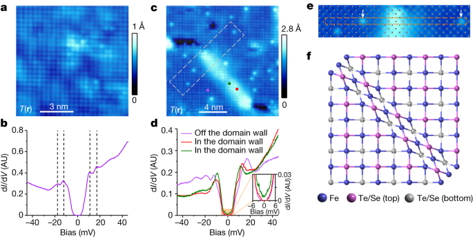
peaks at _Δ_1 ≈ 11 meV and _Δ_2 ≈ 19 meV. E, Waterfall-plot of d_I_/d_V_ curves taken along the light grey arrow in C. EXTENDED DATA FIG. 2 CHARACTERIZATION OF DOMAIN WALLS. A, B, STM
images (16×16 nm2, _V_s = 0.1 V, _I_s = 0.5 nA) of two domain walls labeled as D1 (A) and D4 (B). C, D, d_I_/d_V_ maps of two domain walls. The lattice vectors Q_i,x_(_y_) of two regions
marked by white spots in A and B satisfy Q1_,x_(_y_) = Q2_,x_(_y_). d_I_/d_V_ maps shown in C and D are measured at the red dashed box in A and B, respectively. EXTENDED DATA FIG. 3
NON-DISPERSIVE PDW AND ABSENCE OF PDW IN HIGH ENERGY D_I_/D_V_ MAPS. A, The STM topography of the domain wall D3 shown in Fig. 4. B, The bias dependence of the wavevector of the LDOS
modulation at the domain wall. C,D, d_I_/d_V_ map (C) taken at 80 mV over the same FOV of A and corresponding magnitude of the Fourier transform (D). There is no spatial modulation in the
d_I_/d_V_ map (C) and no FFT peak at around Q ≈ 0.28QFe at the energy much higher than the superconducting gap (D). E,F, Spatial variation of the amplitude (E) and phase (F) of the LDOS
modulation at bias voltage from 0 to 14 mV. The averaging length scales in E and F are denoted by dashed circles. The LDOS modulations mainly exist in the energies within the superconducting
gap, which is also observed at domain wall D2 (Supplementary Fig. 13). Dashed lines in A,C,E and F mark the edges of the domain wall. EXTENDED DATA FIG. 4 DETERMINATION OF MODULATION
WAVEVECTOR Q AT DOMAIN WALL D1. A, The STM topography of the domain wall D1. B, Zero-bias conductance (ZBC) map _g_(R, _V_ = 0 mV) taken at the same area in A. C, The magnitude of the
Fourier transform _g_(Q, _V_ = 0 mV) of the ZBC map in B. D–F, Spatial distribution of the modulation _g_Q(R) phase \({\phi }_{{{\bf{Q}}}_{{\rm{t}}}}^{g}({\bf{r}})\). The averaging length
scales in D–F are denoted by dashed circles. The domain wall area is marked by black dashed lines in A,B and D–F. G–I, Statistical histogram of \({\phi
}_{{{\bf{Q}}}_{{\rm{t}}}}^{g}({{\bf{r}}}_{{\rm{DW}}})\) (RDW represents the area of the domain wall) at the domain wall D1 for a series of tentative Qt. Only the points inside the domain
wall area in D–F are counted. Black dashed lines in G–I are located at the half maximum of the peak. The determined wavevector Q corresponds to the minimum of the full width at half maximum
(FWHM) of the peak in the distribution histogram \({\phi }_{{{\bf{Q}}}_{{\rm{t}}}}^{g}({{\bf{r}}}_{{\rm{DW}}})\), as shown in H. EXTENDED DATA FIG. 5 SUPERCONDUCTING GAP ENERGY MODULATIONS
AT THE DOMAIN WALL LABELED AS D8 IN ANOTHER 1-UC FE(TE,SE)/STO SAMPLE (S2). A, The STM topography of the domain wall. (4.8×4.8 nm2, _V_s = 0.04 V, _I_s = 2.5 nA). B, Spatial distribution of
_Δ_1(R) measured in the same area in A. White dashed lines in B are guides to the eye. C, The magnitude of the Fourier transform of B. Orange crosses are at Q = (±QFe,0), (0,±QFe). The
modulation wavevector Q ≈ ±0.28QFe is marked by dashed blue circles. Black dashed lines in A and B mark the edges of the domain wall. EXTENDED DATA FIG. 6 SPATIAL MODULATIONS OF THE LDOS,
SUPERCONDUCTING GAP ENERGY AND COHERENCE PEAK HEIGHT AT ONE DOMAIN WALL LABELED AS D9 IN ANOTHER 1-UC FE(TE,SE) FILM (S2). A, The STM topography of the domain wall. (4.3×5.4 nm2, _V_s = 0.04
V, _I_s = 2.5 nA). B, d_I_/d_V_ map _g_(R, _V_ = 3 mV) taken at the same area in A. C, The magnitude of the Fourier transform of B. D, Spatial distribution of _Δ_1(R) measured in the same
area in A. E, The magnitude of the Fourier transform of D. F, Spatial distribution of superconducting coherence peak height measured in the same area in A. G, The magnitude of the Fourier
transform of F. H, Line profiles along the (0,0) to (1,0)QFe direction in C, E, and G. Peaks at Q ≈ 0.28QFe appear for all curves. The profiles are normalized and shifted vertically for
comparison. Orange crosses in C, E, and G are at Q = (±QFe,0), (0,±QFe). Black dashed lines in A, B, D and F mark the edges of the domain wall. Orange dashed lines in B, D and F are guides
to the eye. EXTENDED DATA FIG. 7 _Ρ_(R, _V_) MAP (A), CORRESPONDING FOURIER TRANSFORM _Ρ_(Q, _V_) (B), SPATIAL VARIATION OF THE AMPLITUDE \(|{A}_{2{\BF{Q}}}^{\RHO (V)}({\BF{R}})|\) (C) AND
THE PHASE \({\PHI }_{2{\BF{Q}}}^{\RHO (V)}({\BF{R}})\) (D) OF THE 2Q _Ρ_(R) MODULATION AT 2 MV AT THE DOMAIN WALL SHOWN IN FIG. 4 (D3). _ρ_(Q, _V_) exhibits maxima at around ±2Q (marked by
dashed blue circles). The amplitude of the modulation is restricted to the domain wall region and the phase of the 2Q modulation is nearly uniform in the domain wall region, indicating the
existence of the 2Q CDW. The averaging length scales in C and D are denoted by dashed circles. The edge of the domain wall is marked by the dashed lines in A, C and D. EXTENDED DATA FIG. 8
COMPARISON BETWEEN THE ATOMIC LATTICE AND 2Q CDW STATE AT THE DOMAIN WALL SHOWN IN FIG. 4 (D3). A,B, Spatial variation of the phase \({\phi
}_{0.5{{\bf{Q}}}_{{\rm{Fe}}}}^{T}\left({\bf{r}}\right)\) of the STM topology _T_(R) modulation at 0.5QFe (A) and the phase \({\phi }_{2{\bf{Q}}}^{\rho (2{\rm{mV}})}\left({\bf{r}}\right)\) of
the _ρ_(R, _V_ = 2 mV) (charge density) modulation at 2Q (B). Topological defects in A and B are marked by black dots. C,D, Spatial variation of the amplitude
\(\left|{A}_{0.5{{\bf{Q}}}_{{\rm{Fe}}}}^{T}\left({\bf{r}}\right)\right|\) of the STM topology _T_(R) modulation at 0.5QFe (C) and the amplitude \(\left|{A}_{2{\bf{Q}}}^{\rho
(2{\rm{mV}})}\left({\bf{r}}\right)\right|\) of the _ρ_(R, _V_ = 2 mV) modulation at 2Q (D). The spatial variations of the phase and amplitude show many differences between the atomic lattice
and 2Q CDW, indicating that the 2Q CDW is independent of the atomic lattice. The averaging length scales are denoted by dashed circles. The edge of the domain wall is marked by the dashed
lines. EXTENDED DATA FIG. 9 POSSIBLE THEORETICAL SCENARIOS FOR THE PDW STATE AT THE DOMAIN WALL. A, Schematic of the PDW state at the domain wall. \({\varDelta }_{{\rm{SC}}}^{\mathrm{1,2}}\)
and \({\varDelta }_{{\rm{SC}}}^{{\rm{DW}}}\) represent the zero-momentum superconductivity in the domains (1 and 2) and at the domain wall, respectively. B, Illustration of the finite
center of mass momentum, equal-spin pairing in the presence of only Rashba SOC. \({\rm{\langle }}{c}_{{\bf{k}},\uparrow }{c}_{-{\bf{k}}+{\bf{Q}},\uparrow }{\rm{\rangle }}\) and
\({\rm{\langle }}{c}_{-{\bf{k}},\downarrow }{c}_{{\bf{k}}-{\bf{Q}},\downarrow }{\rm{\rangle }}\) are equal-spin pairing order parameters where one spin sector carries momentum +Q and the
other spin sector –Q. C, Illustration of the finite center of mass momentum equal-spin pairing in the presence of both Rashba and Dresselhaus SOC. In this case, the triplet equal-spin
pairing order parameters \({\rm{\langle }}{c}_{{\bf{k}},\sigma }{c}_{-{\bf{k}}+{\bf{Q}},\sigma }{\rm{\rangle }}\) and \({\rm{\langle }}{c}_{-{\bf{k}},\sigma }{c}_{{\bf{k}}-{\bf{Q}},\sigma
}{\rm{\rangle }}\) can have both spin components (_σ_), i.e., each equal-spin pairing sector carries both nonzero momentum +Q and –Q, giving rise to the equal-spin pairing PDW state. D,F,
Calculated tunneling density of states _ρ__i_(_ω_) with _i_ the site index, for two examples with Q = 2π/12 (D) and Q = 2π/4 (F), where the insets show the zoom-in feature around the
coherent peaks. E,G, The spatial modulations of the superconducting gap extracted from the corresponding coherence peak positions for the Q = 2π/12 (E) and Q = 2π/4 (G). SUPPLEMENTARY
INFORMATION SUPPLEMENTARY INFORMATION This file contains Supplementary Text, Figs. 1–20 and References. SOURCE DATA SOURCE DATA FIG. 1 SOURCE DATA FIG. 3 SOURCE DATA FIG. 4 SOURCE DATA FIG.
5 RIGHTS AND PERMISSIONS Springer Nature or its licensor (e.g. a society or other partner) holds exclusive rights to this article under a publishing agreement with the author(s) or other
rightsholder(s); author self-archiving of the accepted manuscript version of this article is solely governed by the terms of such publishing agreement and applicable law. Reprints and
permissions ABOUT THIS ARTICLE CITE THIS ARTICLE Liu, Y., Wei, T., He, G. _et al._ Pair density wave state in a monolayer high-_T_c iron-based superconductor. _Nature_ 618, 934–939 (2023).
https://doi.org/10.1038/s41586-023-06072-x Download citation * Received: 12 September 2022 * Accepted: 11 April 2023 * Published: 28 June 2023 * Issue Date: 29 June 2023 * DOI:
https://doi.org/10.1038/s41586-023-06072-x SHARE THIS ARTICLE Anyone you share the following link with will be able to read this content: Get shareable link Sorry, a shareable link is not
currently available for this article. Copy to clipboard Provided by the Springer Nature SharedIt content-sharing initiative