- Select a language for the TTS:
- UK English Female
- UK English Male
- US English Female
- US English Male
- Australian Female
- Australian Male
- Language selected: (auto detect) - EN
Play all audios:
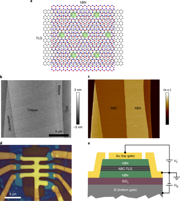
ABSTRACT The Mott insulator is a central concept in strongly correlated physics and manifests when the repulsive Coulomb interaction between electrons dominates over their kinetic energy1,2.
Doping additional carriers into a Mott insulator can give rise to other correlated phenomena such as unusual magnetism and even high-temperature superconductivity2,3. A tunable Mott
insulator, where the competition between the Coulomb interaction and the kinetic energy can be varied in situ, can provide an invaluable model system for the study of Mott physics. Here we
report the possible realization of such a tunable Mott insulator in a trilayer graphene heterostructure with a moiré superlattice. The combination of the cubic energy dispersion in
ABC-stacked trilayer graphene4,5,6,7,8 and the narrow electronic minibands induced by the moiré potential9,10,11,12,13,14,15 leads to the observation of insulating states at the predicted
band fillings for the Mott insulator. Moreover, the insulating states in the heterostructure can be tuned: the bandgap can be modulated by a vertical electrical field, and at the same time
the electron doping can be modified by a gate to fill the band from one insulating state to another. This opens up exciting opportunities to explore strongly correlated phenomena in
two-dimensional moiré superlattice heterostructures. Access through your institution Buy or subscribe This is a preview of subscription content, access via your institution ACCESS OPTIONS
Access through your institution Access Nature and 54 other Nature Portfolio journals Get Nature+, our best-value online-access subscription $29.99 / 30 days cancel any time Learn more
Subscribe to this journal Receive 12 print issues and online access $259.00 per year only $21.58 per issue Learn more Buy this article * Purchase on SpringerLink * Instant access to full
article PDF Buy now Prices may be subject to local taxes which are calculated during checkout ADDITIONAL ACCESS OPTIONS: * Log in * Learn about institutional subscriptions * Read our FAQs *
Contact customer support SIMILAR CONTENT BEING VIEWED BY OTHERS TUNABLE STRONGLY COUPLED SUPERCONDUCTIVITY IN MAGIC-ANGLE TWISTED TRILAYER GRAPHENE Article 01 February 2021 EVIDENCE FOR
UNCONVENTIONAL SUPERCONDUCTIVITY IN TWISTED TRILAYER GRAPHENE Article 15 June 2022 GATE-TUNABLE HEAVY FERMIONS IN A MOIRÉ KONDO LATTICE Article 15 March 2023 DATA AVAILABILITY The data that
support the findings of this study are available from the corresponding authors upon reasonable request. REFERENCES * Mott, N. F. The basis of the electron theory of metals, with special
reference to the transition metals. _Proc. Phys. Soc. Lond. A_ 62, 416–422 (1949). Article ADS Google Scholar * Imada, M., Fujimori, A. & Tokura, Y. Metal–insulator transitions. _Rev.
Mod. Phys._ 70, 1039–1263 (1998). Article ADS Google Scholar * Lee, P. A., Nagaosa, N. & Wen, X. G. Doping a Mott insulator: physics of high-temperature superconductivity. _Rev. Mod.
Phys._ 78, 17–85 (2006). Article ADS Google Scholar * Koshino, M. & McCann, E. Trigonal warping and Berry’s phase _Nπ_ in ABC-stacked multilayer graphene. _Phys. Rev. B_ 80, 165409
(2009). Article ADS Google Scholar * Zhang, F., Sahu, B., Min, H. K. & Macdonald, A. H. Band structure of ABC-stacked graphene trilayers. _Phys. Rev. B_ 82, 035409 (2010). Article
ADS Google Scholar * Bao, W. et al. Stacking-dependent band gap and quantum transport in trilayer graphene. _Nat. Phys._ 7, 948–952 (2011). Article Google Scholar * Lui, C. H., Li, Z.
Q., Mak, K. F., Cappelluti, E. & Heinz, T. F. Observation of an electrically tunable band gap in trilayer graphene. _Nat. Phys._ 7, 944–947 (2011). Article Google Scholar * Zhang, L.
Y., Zhang, Y., Camacho, J., Khodas, M. & Zaliznyak, I. The experimental observation of quantum Hall effect of l = 3 chiral quasiparticles in trilayer graphene. _Nat. Phys._ 7, 953–957
(2011). Article Google Scholar * Yankowitz, M. et al. Emergence of superlattice Dirac points in graphene on hexagonal boron nitride. _Nat. Phys._ 8, 382–386 (2012). Article Google Scholar
* Dean, C. R. et al. Hofstadter’s butterfly and the fractal quantum Hall effect in moiré superlattices. _Nature_ 497, 598–602 (2013). Article ADS Google Scholar * Hunt, B. et al.
Massive Dirac fermions and Hofstadter butterfly in a van der Waals heterostructure. _Science_ 340, 1427–1430 (2013). Article ADS Google Scholar * Ponomarenko, L. A. et al. Cloning of
Dirac fermions in graphene superlattices. _Nature_ 497, 594–597 (2013). Article ADS Google Scholar * Wallbank, J. R., Patel, A. A., Mucha-Kruczynski, M., Geim, A. K. & Falko, V. I.
Generic miniband structure of graphene on a hexagonal substrate. _Phys. Rev. B_ 87, 245408 (2013). Article ADS Google Scholar * Jung, J., Raoux, A., Qiao, Z. & MacDonald, A. H. Ab
initio theory of moiré superlattice bands in layered two dimensional materials. _Phys. Rev. B_ 89, 205414 (2014). Article ADS Google Scholar * Jung, J., DaSilva, A. M., MacDonald, A. H.
& Adam, S. A. Origin of band gaps in graphene on hexagonal boron nitride. _Nat. Commun._ 6, 6308 (2015). Article ADS Google Scholar * Geim, A. K. & Grigorieva, I. V. Van der Waals
heterostructures. _Nature_ 499, 419–425 (2013). Article Google Scholar * Yang, W. et al. Epitaxial growth of single-domain graphene on hexagonal boron nitride. _Nat. Mater._ 12, 792–797
(2013). Article ADS Google Scholar * Shi, Z. et al. Gate-dependent pseudospin mixing in graphene/boron nitride moiré superlattices. _Nat. Phys._ 10, 743–747 (2014). Article Google
Scholar * Mak, K. F., Lee, C., Hone, J., Shan, J. & Heinz, T. F. Atomically thin MoS2: a new direct-gap semiconductor. _Phys. Rev. Lett._ 105, 136805 (2010). Article ADS Google
Scholar * Splendiani, A. et al. Emerging photoluminescence in monolayer MoS2. _Nano. Lett._ 10, 1271–1275 (2010). Article ADS Google Scholar * Rivera, P. et al. Valley-polarized exciton
dynamics in a 2D semiconductor heterostructure. _Science_ 351, 688–691 (2016). Article ADS MathSciNet Google Scholar * Yu, H. Y., Wang, Y., Tong, Q. J., Xu, X. D. & Yao, W. Anomalous
light cones and valley optical selection rules of interlayer excitons in twisted heterobilayers. _Phys. Rev. Lett._ 115, 187002 (2015). Article ADS Google Scholar * Wang, L. et al.
One-dimensional electrical contact to a two-dimensional material. _Science_ 342, 614–617 (2013). Article ADS Google Scholar * Novoselov, K. S. et al. Two-dimensional gas of massless Dirac
fermions in graphene. _Nature_ 438, 197–200 (2005). Article ADS Google Scholar * Zhang, Y. B., Tan, Y. W., Stormer, H. L. & Kim, P. Experimental observation of the quantum Hall
effect and Berry’s phase in graphene. _Nature_ 438, 201–204 (2005). Article ADS Google Scholar * Lee, Y. et al. Competition between spontaneous symmetry breaking and single-particle gaps
in trilayer graphene. _Nat. Commun._ 5, 5656 (2014). Article Google Scholar * Ju, L. et al. Topological valley transport at bilayer graphene domain walls. _Nature_ 520, 650–655 (2015).
Article ADS Google Scholar * Zhang, Y. B. et al. Direct observation of a widely tunable bandgap in bilayer graphene. _Nature_ 459, 820–823 (2009). Article ADS Google Scholar * Hubbard,
J. Electron correlations in narrow energy bands. _Proc. R. Soc. Lond. A_ 276, 238–257 (1963). Article ADS Google Scholar Download references ACKNOWLEDGEMENTS The authors thank C. Jin, E.
Regan, X. Lu, Y. Shan, S. Wu and G. Zhang for discussions and help with sample preparation. The trilayer graphene sample fabrication and experimental study was supported by the Office of
Naval Research (award no. N00014-15-1-2651). The initial idea and proof-of-principle calculation of 2D flatband engineering was supported by an ARO MURI award (W911NF-15-1-0447). Part of the
sample fabrication was conducted at the Nano-fabrication Laboratory at Fudan University. B.L.C. was supported by the Basic Science Research Program through the National Research Foundation
of Korea (NRF) funded by the Ministry of Education (2018R1A6A1A06024977) and by grants NRF-2016R1A2B4010105 and NRF-2017R1D1A1B03035932. J.J. was supported by the Samsung Science and
Technology Foundation under project no. SSTF-BA1802-06. Y.Z. acknowledges financial support from the National Key Research Program of China (grant nos. 2016YFA0300703 and 2018YFA0305600),
the NSF of China (grant nos. U1732274, 11527805, 11425415 and 11421404), Shanghai Municipal Science and Technology Commission (grant no. 18JC1410300) and the Strategic Priority Research
Program of the Chinese Academy of Sciences (grant no. XDB30000000). Z.S. is supported by the Program for Professor of Special Appointment (Eastern Scholar) at Shanghai Institutions of Higher
Learning and the National Natural Science Foundation of China under grant no. 11574204. B.L., H.L. and Z.S. are supported by the National Key Research and Development Program of China
(grant 2016YFA0302001) and National Natural Science Foundation of China (grants 11574204, 11774224). Growth of hBN crystals was supported by the Elemental Strategy Initiative conducted by
the MEXT, Japan and JSPS KAKENHI grant no. JP15K21722. Part of the sample fabrication was conducted at Fudan Nano-fabrication Lab. AUTHOR INFORMATION AUTHORS AND AFFILIATIONS * Department of
Physics, University of California at Berkeley, Berkeley, CA, USA Guorui Chen, Lili Jiang & Feng Wang * State Key Laboratory of Surface Physics and Department of Physics, Fudan
University, Shanghai, China Guorui Chen & Yuanbo Zhang * Collaborative Innovation Center of Advanced Microstructures, Nanjing, China Guorui Chen, Bosai Lyu, Hongyuan Li, Zhiwen Shi &
Yuanbo Zhang * Department of Electrical Engineering and Computer Sciences, University of California, Berkeley, CA, USA Shuang Wu * Key Laboratory of Artificial Structures and Quantum
Control (Ministry of Education), School of Physics and Astronomy, Shanghai Jiao Tong University, Shanghai, China Bosai Lyu, Hongyuan Li & Zhiwen Shi * Department of Physics, University
of Seoul, Seoul, Korea Bheema Lingam Chittari & Jeil Jung * National Institute for Materials Science, Tsukuba, Japan Kenji Watanabe & Takashi Taniguchi * Institute for Nanoelectronic
Devices and Quantum Computing, Fudan University, Shanghai, China Yuanbo Zhang * Materials Science Division, Lawrence Berkeley National Laboratory, Berkeley, CA, USA Feng Wang * Kavli Energy
NanoSciences Institute at the University of California, Berkeley and the Lawrence Berkeley National Laboratory, Berkeley, CA, USA Feng Wang Authors * Guorui Chen View author publications
You can also search for this author inPubMed Google Scholar * Lili Jiang View author publications You can also search for this author inPubMed Google Scholar * Shuang Wu View author
publications You can also search for this author inPubMed Google Scholar * Bosai Lyu View author publications You can also search for this author inPubMed Google Scholar * Hongyuan Li View
author publications You can also search for this author inPubMed Google Scholar * Bheema Lingam Chittari View author publications You can also search for this author inPubMed Google Scholar
* Kenji Watanabe View author publications You can also search for this author inPubMed Google Scholar * Takashi Taniguchi View author publications You can also search for this author
inPubMed Google Scholar * Zhiwen Shi View author publications You can also search for this author inPubMed Google Scholar * Jeil Jung View author publications You can also search for this
author inPubMed Google Scholar * Yuanbo Zhang View author publications You can also search for this author inPubMed Google Scholar * Feng Wang View author publications You can also search
for this author inPubMed Google Scholar CONTRIBUTIONS F.W. and Y.Z. supervised the project. G.C. fabricated samples and performed transport measurements. G.C., L.J., S.W., B.L., H.L. and
Z.S. prepared trilayer graphene and performed near-field infrared and atomic force microscopy measurements. B.L.C. and J.J. calculated the band structures. K.W. and T.T. grew hBN single
crystals. G.C., Y.Z. and F.W. analysed the data. CORRESPONDING AUTHORS Correspondence to Yuanbo Zhang or Feng Wang. ETHICS DECLARATIONS COMPETING INTERESTS The authors declare no competing
interests. ADDITIONAL INFORMATION PUBLISHER’S NOTE: Springer Nature remains neutral with regard to jurisdictional claims in published maps and institutional affiliations. SUPPLEMENTARY
INFORMATION EXTENDED DATA Extended data figures 1–7; references 30–35 RIGHTS AND PERMISSIONS Reprints and permissions ABOUT THIS ARTICLE CITE THIS ARTICLE Chen, G., Jiang, L., Wu, S. _et
al._ Evidence of a gate-tunable Mott insulator in a trilayer graphene moiré superlattice. _Nat. Phys._ 15, 237–241 (2019). https://doi.org/10.1038/s41567-018-0387-2 Download citation *
Received: 01 November 2018 * Accepted: 27 November 2018 * Published: 21 January 2019 * Issue Date: March 2019 * DOI: https://doi.org/10.1038/s41567-018-0387-2 SHARE THIS ARTICLE Anyone you
share the following link with will be able to read this content: Get shareable link Sorry, a shareable link is not currently available for this article. Copy to clipboard Provided by the
Springer Nature SharedIt content-sharing initiative