- Select a language for the TTS:
- UK English Female
- UK English Male
- US English Female
- US English Male
- Australian Female
- Australian Male
- Language selected: (auto detect) - EN
Play all audios:
ABSTRACT One of the main challenges in stretchable electronics is to achieve high-performance stretchable semiconductors. Here, we introduce an innovative concept of nanomeshed semiconductor
nanomembrane which can be regarded almost as intrinsically stretchable to conventional microelectronic layouts. By making a silicon film into homogeneous nanomeshes with spring-like nano
traces, we demonstrated a high electron mobility of 50 cm2/V·s, and moderate stretchability with a one-time strain of 25% and cyclic strain of 14% after stretching for 1000 cycles, further
improvable with optimized nanomesh designs. A simple analytic model covering both fractional material and trace sidewall surfaces well predicted the transport properties of the normally on
silicon nanomesh transistors, enabling future design and optimizations. Besides potential applications in stretchable electronics, this semiconductor nanomesh concept provides a new platform
for materials engineering and is expected to yield a new family of stretchable inorganic materials having tunable electronic and optoelectronic properties with customized nanostructures.
SIMILAR CONTENT BEING VIEWED BY OTHERS HIGHLY STRETCHABLE POLYMER SEMICONDUCTOR THIN FILMS WITH MULTI-MODAL ENERGY DISSIPATION AND HIGH RELATIVE STRETCHABILITY Article Open access 16
December 2023 FULL INTEGRATION OF HIGHLY STRETCHABLE INORGANIC TRANSISTORS AND CIRCUITS WITHIN MOLECULAR-TAILORED ELASTIC SUBSTRATES ON A LARGE SCALE Article Open access 01 April 2024 A
DESIGN STRATEGY FOR HIGH MOBILITY STRETCHABLE POLYMER SEMICONDUCTORS Article Open access 11 June 2021 INTRODUCTION Stretchable electronics have emerged as promising platforms for many
important areas such as bio-mimetics, health monitoring, biomedical therapeutics, and soft robotics.1,2,3,4,5,6 Due to their low modulus, these stretchable platforms can either serve as
artificial electronic organs or form more conformal and compatible interface with irregular, shape-evolving or soft objects.7,8,9 Compelling examples of such applications include electronic
skin demonstrations from various stretchable active matrices10,11,12 and multifunctional balloon catheters for cardiac electrophysiological mapping and ablation therapy.13,14,15,16
Historically, core material elements in conventional high-performance electronics are inorganic single crystals such as silicon (Si) or compound semiconductors, which arguably laid the
foundation for modern society.17,18,19 However, those materials are usually rigid. Great efforts have made these semiconductors in thin film structures and render them flexible, but they are
still brittle, making it difficult to achieve stretchable devices. Seeking stretchable electronic components, especially stretchable semiconductors with high performance, therefore, has
been one of the critical challenges in achieving next-generation stretchable electronics. In the past decade, there has been significant progress in realizing stretchable semiconductors,
mainly from two complementary ways. One approach involves designing novel microstructural layouts in standard materials, as exemplified by configuring inorganic semiconductor based circuits
into microscale island-bridge layout.20,21,22,23 The other centers in developing intrinsically stretchable components such as organic semiconductors24,25,26,27 and nano-wire or nano-tube
networks.28,29,30 Among all existing approaches, microscale structuring often lacks the high-density advantage in modern microelectronics, which has been exploited to the extreme level under
what’s commonly known as Moore’s law. On the other hand, intrinsically stretchable semiconductors currently are still quite limited in their mobility and/or reliability, with typical
electron mobility still less than 10 cm2/V·s,31,32,33 while bottom up assembled networks such as carbon nanotube webs are limited by their uniformity.34,35 Existing approaches are still
incompetent when high-density, high-performance stretchable electronics are needed. Here, using Si as a model system we conceptualize and demonstrate a new stretchable semiconductor
platform, namely nanomeshed Si nanomembranes. The nanomeshed nanomembrane is a dense network of fully connected, single-crystalline Si traces of nanoscale line-width and thickness. Due to
their spring-like traces, the semiconductor nanomeshes possess promising stretchability while with high electrical performance and high scalability to microscale footprints. This latter
property renders semiconductor nanomeshes almost as intrinsically stretchable for microelectronic layouts. As a proof of concept, we achieved nanomeshes of Si with tunable trace widths from
a lift-off and transfer process using a Si-on-insulator (SOI) wafer, with nanomesh pattern defined by two different soft lithography methods. To facilitate the nanomesh transfer and provide
additional mechanical support, we further introduced a bilayer structure of Polyimide (PI)/Si nanomeshes on elastomer substrates to improve the stretchability. The Si nanomesh film with a
peak effective mobility of 50 cm2/V·s has demonstrated a one-time stretchability of up to 25% strain, and robust cyclic stretchability with less than 10% fatigue after 1000 stretching cycles
with a constant strain of 14%. An analytical model coupling factors from both the fractional material and trace sidewall surfaces predicted the mobility trend of the Si-nanomesh transistors
as a function of fractional Si, indicating that the mobility can be enhanced with future surface passivation. Together these results demonstrate nanomeshing semiconductors as a unique and
promising pathway towards high-density, high-performance stretchable microelectronics. RESULTS MATERIALS CHARACTERIZATION AND FABRICATION OF STRETCHABLE SINGLE-CRYSTALLINE NANOMESHED SI
NANOMEMBRANES The nanomeshes consist thin, curvilinear nano-traces of single-crystalline Si densely connected with each other, and they can be bonded onto Polydimethylsiloxane (PDMS) or
other elastomer substrates with Si–O chemical bonding for mechanical support. The mechanical, electrical and other properties of the Si nanomeshes are expected to be determined by the
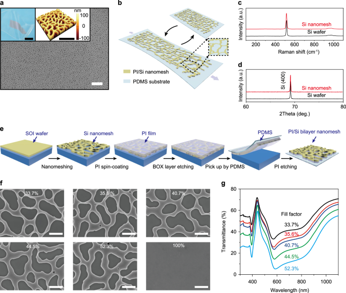
properties of the original Si and the structure of the nanomeshes. As shown in the photograph and images from atomic force microscopy (AFM) and scanning electron microscopy (SEM) (Fig. 1a),
the Si nanomeshes can be achieved at cm scale with high uniformity and without any missing traces. Figure 1b illustrates the schematic of a stretchable Si-nanomesh film. These spring-like
traces can be deformed to accommodate the applied strain which makes the nanomesh network stretchable. Here, an additional PI layer also exists underneath the Si, forming bilayer nanomeshes,
further providing mechanical support. Figure 1c presents the Raman spectra of the Si nanomeshes and a single-crystalline Si (sc-Si) wafer. The transverse optical (TO) Raman peak is observed
at 520 cm−1, which is in good agreement with sc-Si. X-ray diffraction (XRD) characterization (Fig. 1d) shows that Si nanomeshes also have the same strong and sharp diffraction peak from the
(400) plane of Si as sc-Si with comparable values of full width at half maximum (FWHM) of 0.16° for Si nanomeshes and 0.12° for Si wafer. The XRD and Raman results confirm the
single-crystalline nature of the Si nanomesh traces, which is critical to achieving superior carrier transport properties. To fabricate stretchable Si nanomeshes, we first patterned the Si
film into nanomeshes in the SOI source wafer, then transferred them onto a PDMS substrate (Fig. 1e). Here, we modified the Indium (In) grain boundary lithography method36,37 as an exemplar,
large-scale, soft lithography approach to form the Si nanomesh pattern. This process utilizes self-formed In grain boundaries to achieve Cr nanomeshes on the source SOI wafer (Si thickness,
_t_Si = 145 nm), followed by Si dry etching with Cr nanomeshes as the mask (Supplementary Fig. 1). Removal of Cr completes the fabrication of Si nanomeshes in the SOI wafer. After the Si
nanomesh formation, a simple transfer process achieves freely stretching Si nanomeshes onto PDMS substrates (Fig. 1e). An ultrathin PI layer secures the Si nanomeshes during the transfer
process. After being picked by PDMS substrate, the PI layer was patterned by using Si nanomeshes as a self-aligned mask. The PI layer finally forms a bilayer nanomesh structure with Si,
providing additional support for the Si nanomeshes during mechanical deformation. Detailed fabrication parameters can be found in the Methods section. We envision that similar fabrication
processes can be applicable to a variety of other semiconductors and inorganic materials. The trace width of Si nanomeshes can be tailored from this fabrication process (Supplementary Fig.
2). The SEM images of the Si nanomeshes with different trace widths and fill factors (defined by the occupation percentage of Si in the nanomeshes over a given microscale area, e.g., 10 × 10
µm2) are shown in Fig. 1f, along with the image of a Si full film. As another proof of concept, we also demonstrated free-standing, non-stretchable Si nanomeshes from nanosphere lithography
with circular nanomesh openings (Supplementary Fig. 3). We note that previously non-free-standing Si nano-networks have been achieved for thermoelectric applications by either a
superlattice nanowire lithography technique or electron-beam lithography,38,39 however, there has not been any work in utilizing substrate-detached semiconductor nanomeshes for stretchable
electronics nor studying relevant properties. OPTICAL PROPERTIES OF SI NANOMESHES The optical transmittance measurement reveals the optical properties of Si nanomeshes, which are transferred
onto glass substrates for easy handling. Figure 1g illustrates transmittance spectra of Si nanomeshes with different fill factors in the wavelength ranging from 300 to 1100 nm. There are
two prominent trends as the fill factor changes. First, as expected, the transmittance increases as the fill factor decreases, since there are less Si to absorb light. As a result, the
transmittance of Si nanomeshes with the fill factor of 33.7% is larger than 35% over the entire measurement window. Compared with the transmittance spectra of a Si full film transferred from
the same SOI wafer (Supplementary Fig. 4), transmittance through Si nanomeshes in certain wavelength regimes is lower, largely owing to the larger reflection from the textured surface of
the nanomeshes. Second, both the absorption peak at 400 nm and 600 nm show blue shifts with decreasing fill factor. These shifts are intriguing, given that trace widths are on the order of a
couple of hundred nm, and well above the exciton Bohr radius of Si (~only a few nm), therefore the quantum confinement effects should not be dominating. We attribute this phenomenon to the
change of the volume modes of the Si trace dielectric waveguides. Indeed, previous theoretical and experimental studies on Si nanowires reveal that the wavelength _λ_ of the photonic modes
in the nanowires scale proportionally with their diameter _d_, with the position of the absorption peaks all moving to high energies when decreasing the nanowire diameter.40 To a certain
extent, the Si nanomeshes can be regarded as a network of nanoscale traces which are similar to nanowires. The exact relationship between _λ_ and the trace width is yet to be determined in
the nanomesh case here by considering the large variation in the trace width (as shown in Supplementary Fig. 2a), as well as the curvilinear nature of the nanoscale traces. However, the
shift directions are the same between nanomeshes and nanowire arrays. Transmittance result of the circular nanomesh (Supplementary Fig. 5) also reveals similar trends. TRANSPORT PROPERTIES
OF NANOMESHED SI NANOMEMBRANES To study the carrier transport properties of Si nanomeshes, we fabricated and investigated N-channel metal-oxide-semiconductor (NMOS) transistors based on Si
nanomeshes (Fig. 2a). Devices are made and studied on the SOI source wafer for easy gating while still revealing nanomesh properties. The source and drain nickel (Ni) contacted Si parts are
heavily n-type doped and the channel is lightly p-type doped. Gate voltage is applied from the Si handle wafer with the 120-nm-thick BOX layer as the gate dielectric. The sheet resistance
and contact resistance of the Si nanomesh transistor are 29.05 kΩ/sq and 2.16 kΩ, respectively, which are calculated through the transmission line measurement (Supplementary Fig. 6). The
results are similar to those of previous poly-Si nanosheet transistors with nickel silicide contact after channel width normalization.41 The transfer characteristics of a Si-nanomesh (52.3%
fill factor) transistor (channel length _L_ = 40 μm, width _W_ = 35 μm) exhibit a clear NMOS switching behavior, with a high ON/OFF current ratio (_I_ON/_I_OFF) of over 105 (Fig. 2b). Above
the threshold voltage (_V_th) of −1.5 V, the drain current (_I_d) increases nearly linearly as gate voltage (_V_g) increases, indicating that neither the mobility (_µ_) is degrading at high
electrical field nor the contact resistance is limiting the current conduction. The device exhibits clearly linear _I-V_ characteristics at low drain voltage (_V_d) region, also indicating
Ohmic S/D contacts (Fig. 2c). The current saturation at high _V_d region also matches with typical long-channel transistor behaviors. The OFF-state currents will not be influenced by the
nanomesh fill factor, while the ON-state current increases with the fill factor, resulting in a small increase of the _I_ON/_I_OFF ratio (Supplementary Figs 7 and 8). Figure 2d presents
extracted effective mobilities as a function of the gate voltage for nanomeshes with different fill factors. The transistor extracted parameter for the mobility calculation are summarized in
the Supplementary Table 1. The mobility of all Si nanomeshes first increase at low values of _V_g, then reach a peak, and finally decrease, consistent with a typical screening-scattering
transition. Notably, we achieved peak effective mobilities from 50 cm2/V·s to 95 cm2/V·s at fill factor from 33.7% to 52.3%. The mobilities of Si nanomeshes are smaller than values expected
from a ‘dilution’ perspective from the full-film Si transistor (with _µ_ ~ 615 cm2/V·s, see Supplementary Fig. 9), where we can simply calculate the mobility of Si nanomeshes from
multiplying the mobility of Si full film by the Si fill factor in the nanomesh. However, they are significantly higher compared to other stretchable semiconductors, where the mobilities are
typically much less than 10 cm2/V·s. Understanding the fundamental transport properties therefore is encouraging to exploit the full potential of semiconductor nanomeshes. MODELING OF THE
CARRIER TRANSPORT IN NANOMESHED SI NANOMEMBRANES The mobility deviation of Si nanomeshes from the simple dilution perspective is intriguing. To shed light on the structure-property
relationship of Si nanomeshes regarding their carrier transport properties, we constructed a simple analytical model, where the key point is to consider the Si-nanomesh film as a new
material (Fig. 3a). The structure of a Si-nanomesh film will be determined by its nanomesh pattern, trace width, in addition to the Si film thickness. We hypothesize that there are two
factors that mainly contribute to the nanomesh mobility: one is the fractional Si material, the other is the surface scattering from the sidewalls of the nanoscale traces. To simplify the
analysis, we consider a Si-nanomesh film with a fixed nanomesh pattern and film thickness, while with shrinking trace width. As the trace width decreases, the fractional Si material reduces,
which is represented by the shrinking of the blue area in Fig. 3a. If we denote _x_ as the fill factor of Si in the _W_ × _L_ channel area, neglecting the scattering from the trace
sidewalls, the fractional-material induced mobility (_µ_fill) can be calculated as _a_×_x_ to the first order as we have discussed in the dilution perspective, where _a_ is a constant with a
value equal to full film mobility, _µ_full-film. On the other hand, there are increasing sidewall areas if the nanomesh trace narrows. Assuming all nanomesh openings have the same shape for
in the entire _W_ × _L_ area, the sidewall area (_s_), equal to the sidewall circumference times the film thickness, will therefore be proportional to the square root of (1 _–_ _x_). If
assuming proportional scattering from the sidewall, the sidewall-area induced mobility (_µ_wall) will then be \(b/\sqrt {1 - x}\), where _b_ is a prefactor related with sidewall surface
quality. To include effects from both the fractional material and trace sidewall scattering, we approximate the combination of their influences by using “Matthiessen’s Rule”: $$\frac{1}{\mu
} = \frac{1}{{\mu _{fill}}} + \frac{1}{{\mu _{wall}}}$$ (1) where _µ_ is the mobility of the Si nanomesh film. Thus, the dependence of mobility of Si nanomeshes on the Si fill factor can be
expressed as: $$\mu = \frac{{abx}}{{ax\sqrt {1 - x} + b}}$$ (2) Figure 3b plots the relative mobility curves (_µ_/_µ_full-film) as a function of fill factor (_x_) with different _a_, _b_
values. When the mobility is only dominated by the fractional material (i.e., _b_ = _∞_), there is a linear relationship between mobility and fill factor as expected. When considering the
sidewall surface scattering (finite _b_ values), the mobility shows a sharp decrease as the fill factor reduces. The more the sidewall surface scattering is (decreasing _b_ value), the
faster the drop of the nanomesh mobility will be, especially in the initial decrease in the fill factor. To validate our analytical model, we fit the model to the experimental dependence of
peak effective mobility on fill factor _x_. The curve extracted from Eq. (2) with _a_ = 616.3 cm2/V·s and _b_ = 71.8 cm2/V·s is in good agreement with the experimental data (Fig. 3c). This
agreement strongly encourages the idea of incurring trace sidewall scattering for carrier transport studies in nanomesh films. This modeling result also suggests that the mobility can be
further improved by future surface passivation, which can reduce the trace sidewall surface scattering. The mobility of circular nanomesh transistors shows a similar trend with the ones made
by the In grain boundary lithography, and an analytical model with _a_ = 615.9 cm2/V·s and _b_ = 94.6 cm2/V·s well fits with the experimental results, validating our approach (Supplementary
Fig. 10). MECHANICAL STRETCHABILITY OF TRANSFERRED SI NANOMESHES ON PDMS Finally, the bilayer PI/Si nanomeshes also demonstrate promising stretchability. Here a customized automatic
stretcher (Supplementary Fig. 11) characterizes the stretchability of the Si nanomeshes. The test was performed at a low speed of 0.05 mm/s to avoid any abrupt strain caused by the high
stretching speed. Figure 4a plots the dependence of sheet resistance on tensile strain for PI/Si nanomeshes of 33.7% fill factor on a 1-mm-thick PDMS substrate. The sheet resistance
increases nonlinearly as tensile strain with two obvious tendencies. When the strain is smaller than ~20%, the sheet resistance remains nearly unchanged, while at higher strain state a fast
increase in resistance occurs. At a small global strain, the nanomesh traces can deform within the plane without exceeding the Si fracture strain limit. Indeed, as shown in the inset SEM
image of 14% strain state in Fig. 4a, nearly no cracks or broken traces are observed. The resistance slightly increases in the strain range of 10 to 20%, which may arise from the
piezoresistive effect of Si. When the global strain is large, nonreversible breaking of Si traces occurred, as observed from the SEM image of the nanomeshes at a 28% strain state in Fig. 4a.
On the other hand, the low-strain stretching is reversible and repeatable. Figure 4b shows the fatigue test with up to 1000 stretching cycles at a 14% strain. No obvious fatigue from the
sheet resistance change is observed after the cyclic stretching up to 1000 cycles. Since Si usually fractures at ~1% strain, this 14% stretchability has already achieved an order of
magnitude increase of the performance. Both theoretical and finite element analysis (FEA) models are developed to reveal the advantageous mechanical stretchability of the bilayer PI/Si
structure. The models consist of a Si layer of thickness _t_Si, a PI layer of the thickness _t_PI and a PDMS substrate that is assumed to be very soft and infinitely thick as compared to the
PI or the Si layers as shown in Fig. 4c. The loading is considered to be at the bottom of the PI layer where an applied strain _ε_applied extends the original length _l_0 to the deformed
length of _l_0_ε_applied. As _l_0 approaches zero, this model gives the effects of a localized strain. For the theoretical model, the interaction between the PDMS and the bilayer structure
is neglected, and the bilayer structure is modeled as a composite beam (equivalent tensile stiffness _K_eff, bending stiffness _B_eff, and the neutral axis position _h_N can be obtained
analytically.42 The strain in the structure consists of the membrane and bending stress, and the total maximum strain is found to be at the interface between the Si and the PI layers, with
the normalized magnitude of $$\frac{{\varepsilon _{\max }}}{{\varepsilon _{\max 0}}} = 1 - \frac{{t_{{\mathrm{PI}}}}}{{t_{{\mathrm{Si}}}}}\left( {\frac{{h_{\mathrm{N}}}}{{t_{{\mathrm{Si}}}}}
+ \frac{{12B_{{\mathrm{eff}}}}}{{K_{{\mathrm{eff}}}h_{\mathrm{N}}t_{{\mathrm{Si}}}}}} \right)^{ - 1}$$ (3) where _ε_max0 is the maximum strain in Si when _t_PI = 0. Figure 4d shows the
comparison between the results given by Eq. (3) (solid line) and the results given by a 2D finite element model that considers the PDMS substrate, adopting the experimental data of _E_Si =
160 GPa, _ν_Si = 0.22, _E_PI = 2.5 GPa, _ν_PI = 0.3 (_E_, Young’s modulus; _ν_, Poisson’s ratio).43,44 The analytical model predicts the maximum strain in the Si layer very well. Figure 4d
also shows that a thicker PI layer significantly reduces the strain in the Si layer, thereby promoting stretchability. For example, when _t_PI = 10·_t_Si, the maximum strain in the silicon
is reduced by ~50 times as compared with a structure without the PI layer. This stretchability enhancement in the bilayer nanomesh structure is because the PI nanomesh can prevent the strain
localization and redistribute the deformation in the Si traces to make stress uniform. The FEA model with _t_Si = 145 nm and _t_PI = 300 nm is shown in Fig. 4e to further reveal the
strain-stress behavior of the Si nanomeshes. When the nanomeshes are stretched, the stress is distributed in the entire bilayer nanomeshes. Due to the spring-like nano traces, the average
stress in the nanomesh film is modest (less than 1 GPa) even at a 20% strain, consistent with our experimental results. With the global strain increasing (to 40% strain, Fig. 4e), the local
stress of some traces in the parallel direction becomes greater than its fracture stress of ~2 GPa,45 leading to possible fractures and a sharp, non-reversible increasing of resistance. This
FEA analysis evidently reveals that nanoscale spring-like traces can effectively endure large global strain in semiconductor nanomeshes. Clearly, this stretching behavior will be heavily
geometry dependent and we expect the stretchability of Si nanomeshes can be improved by forming more-stretchable patterns in future nanomesh traces. DISCUSSION The results presented here
demonstrated a new material platform—nanomeshed Si nanomembranes—which are stretchable while with superior carrier transport properties. Devices such as stretchable diodes with large area
coverages and/or high densities can be readily achieved, in a way that leverages both metal and semiconductor nanomeshes and conventional microelectronic layout. Future efforts have the
potential to engineer the nanomesh pattern and materials surfaces to maximize the performance from Si nanomesh devices. For example, we envision that many previous design concepts such as
the horseshoe and serpentine structures46,47 in microscale wavy structures, and the fractal design48,49 can also apply to semiconductor nanomeshes for the enhancement of their
stretchability. Key challenges to be addressed may lie in developing the fabrication methods to achieve the large-scale semiconductor nanomeshes with user-defined patterns of feature size
down to the nanometer regime and at low cost. While using SOI can be uneconomic for many applications, there are certain areas such as in biomedical and clinical applications where the
devices from this process could still be affordable. Future process development to replace the SOI process include utilizing deposited amorphous-Si layers as the active material
(Supplementary Fig. 12), or transferring Si ribbons from bulk wafers50 then converting to nanomeshes (Supplementary Fig. 13). Stretchable dielectrics are currently limited by their large
leak current, small capacitance and poor environmental robustness. Parallel efforts should also focus on developing nanomesh compatible stretchable thin dielectrics and device
miniaturization to fully enable nanomesh-based active electronics. This nanomesh approach is readily applicable to other inorganic materials such as optoelectronic semiconductors (e.g.,
gallium nitride) and piezoelectric materials (e.g., lead zirconate titanate) to enable stretchability. This work is expected to spur a stream of both fundamental and applied research on
nanomeshed forms of existing and new electronic materials. METHODS PATTERNING OF SI NANOMESHES IN A SOI SOURCE WAFER As shown in Supplementary Fig. 1, the nanomesh patterning started with a
silicon-on-insulator (SOI) wafer which was commercially available (SIMOX SOI, distributed by University Wafer). The SOI wafer consisted of a top Si layer that was a single-crystalline Si
with (100) crystal orientation, lightly p-type doped with a doping concentration of 1 × 1014 cm−3 and a thickness of 145 nm. The buried oxide layer was 120 nm thick, and the handle wafer was
750 μm thick. In principle, the Si nanomeshes can be achieved through various lithography processes, including electron-beam (e-beam) lithography, stepper lithography, In grain boundary
lithography, and anodized-aluminum-oxide template lithography. Here in the patterning process, a Poly(methyl methacrylate) (PMMA) thin film with 500 nm thickness first coated the pre-cleaned
SOI wafer. Electron beam (e-beam) evaporation then yielded a 2-nm-thick titanium (Ti) adhesion layer and 20-nm-thick SiO2 thin film on the PMMA layer. This PMMA layer was to serve as a
lift-off resist under the to-be-deposited In grains and the Ti/SiO2 layer is for a better wetting of In to form irregular grains instead of circular ones. E-beam evaporation then yielded an
In film with a thickness of 250 nm, followed by a 20% HNO3 wet etching to control the gap between grains. The In grain etching process was an isotropic process, including surface oxidation
and acidic etching. The acidic etching was a fast process while the surface oxide layer prevented In from etching away, making the etching rate always under control. Here, the In grains
defined the pattern of the final Si nanomeshes, while the gaps between In grains after the HNO3 etching process determined the Si trace width. After forming clear In grain boundaries,
inductive coupled plasma (ICP) (Plasma-Therm, 790) dry etching processes selectively etched the SiO2 and PMMA layer to expose the SOI wafer under the grain boundary. E-beam evaporation then
formed a 30-nm-thick Cr film on the exposed Si. Immersing the wafer in acetone dissolved the PMMA and lift off the In grains and Ti/SiO2 wetting layer, with the help of a gentle sonication.
The steps mentioned above formed a Cr nanomesh mask on top of the SOI wafer, which served as the master pattern to achieve the final Si nanomeshes. ICP Si dry etching process then etched the
Si in the SOI wafer with Cr nanomesh mask. Finally a Cr etchant (Transene, 1020AC) removed the Cr nanomesh mask, leaving only Si nanomeshes on the SOI wafer. The Cr mask should be removed
immediately to avoid the oxidation of Cr. The thickness of top Si layer therefore defined the Si nanomesh thickness. FABRICATION OF SILICON-NANOMESH TRANSISTORS First, plasma-enhanced
chemical vapor deposition (PECVD) (SPTS, LpX) deposited a 300 nm-thick SiO2 film on the SOI wafer as the doping mask. Conventional photolithography then defined the source and drain
patterns, followed by the SiO2 film etching by a trifluoromethane (CHF3) plasma in ICP system. The diffusion of phosphorus (Filmtronics, P451) then occurred at 950 °C for 5 min in a tube
furnace (Thermco, MB-71 Mini Brute Tube). The doping concentration here was quantified from 4-point-probe measurements to be ~6 × 1019 cm–3. After the doping, immersing the wafer in 20% HF
for 10 s etched SiO2 mask film. The process of patterning Si nanomeshes mentioned above was then conducted on the post-doping SOI wafer. After the nanomesh formation, photolithography then
defined the transistor area, and an ICP etching with sulfur hexafluoride (SF6) gas isolated the transistor. E-beam evaporation then yielded Ni layer with a thickness of 100 nm to form
contacts with heavily doped Si parts, with photolithography defining the source and drain regions. Immersing the wafer in 30 wt.% iron (III) chloride (FeCl3) solution for 20 s finally
isolated Ni contact and completed the back-gated transistor fabrication. EFFECTIVE MOBILITY OF SILICON-NANOMESH TRANSISTORS The effective mobility of Si-nanomesh transistors was extracted
from their transfer characteristics curves by using the equation, $$\mu = \frac{L}{{WC_{ox}(V_g - V_{th} - 0.5V_d)}}\frac{{\partial I_d}}{{\partial V_{\mathrm{g}}}}$$ (4) where _C_ox
represents the gate capacitance which is calculated from a parallel plate model. Note that the _W_ here is defined as the overall device width, instead of the sum of the Si nanomesh trace
widths, since we regard the Si-nanomesh film effectively as a new material. TRANSFER OF STRETCHABLE PI/SI BILAYER NANOMESHES ON A PDMS SUBSTRATE Before the transfer process, a high
temperature doping step doped the top Si layer in the SOI wafer to a doping concentration of ~5 × 1018 cm−3. The aforementioned soft lithography process then patterned the doped Si into
nanomeshes on the SOI wafer. To facilitate the transfer, a 300-nm-thick PI film coated on the post-nanomeshing SOI wafer, followed by curing at 250 °C for 90 min. Immersing the wafer in 20%
HF for 1 min then undercut the buried oxide layer through the ultrathin PI layer. Before the lift-off of the PI layer embedding the Si nanomeshes, e-beam evaporation yielded a thin layer of
Ti/SiO2 on the PI film. In parallel, a PDMS elastomer base was mixed at a 10:1 ratio with the curing agent, followed by curing at 80 °C for 1 h to prepare the PDMS receiving substrate. A
1-mm-thick PDMS substrate with a pre-treatment by UV-O3 plasma for 15 min then picked up the PI layer with Si nanomeshes embedded. After this step, the Si nanomeshes and PI layer were
flipped over, resulting that the Si nanomeshes were on top of the PI layer. Finally, an ICP RIE step with O2 plasma patterning the PI layer with Si nanomeshes as the self-aligned etching
mask completed the formation of the stretchable PI/Si nanomeshes on PDMS. STRETCHING EXPERIMENTS The engineering strain was utilized to characterize the stretchability. The strain (_e_) can
be calculated as \(e = \frac{{{\mathrm{\Delta }}L}}{L} = \frac{{l \,-\, L}}{L}\), where _L_ and _l_ are the length of stretchable area in the original and stretching status, respectively.
Each stretching cycle consists of one stretching immediately followed by one releasing movement. The test was performed at a low speed of 0.05 mm/s to avoid the external effects caused by
the high stretching speed. After the transfer process, the UV-O3 plasma treated the back side of the PDMS substrate. Two glass pieces fixed the two ends of the PDMS substrate with the
nanomesh film by the Si–O bonding, and a 1-cm-wide gap in between the glasses allowed for stretching tests. The sheet resistance during stretching was measured by using the four point probe
method. MATERIALS CHARACTERIZATION OF SI NANOMESHES We took the morphology and topographic images of the nanomeshes utilizing the scanning electron microscope (Zeiss, Supra 25) and atomic
force microscope (Park systems, XE7), respectively. A Raman system (Renishaw) with the 488 nm laser measured Raman spectrum of the nanomeshes. A UV-visible spectrometer (PerkinElmer, Lambda
35) recorded optical spectra in the wavelength range from 300 to 1100 nm. A probe station (EverBeing Int’l corp) connected with a semiconductor analyzer (Keysight, B1500A) measured transport
properties of nanomesh transistors. DATA AVAILABILITY The data that support the findings of this study are available from the corresponding author upon reasonable request. REFERENCES * Kim,
D. H. et al. Dissolvable films of silk fibroin for ultrathin conformal bio-integrated electronics. _Nat. Mater._ 9, 511–517 (2010). Article CAS Google Scholar * Kim, D. H. et al.
Epidermal electronics. _Science_ 333, 838–843 (2011). Article CAS Google Scholar * Schwartz, G. et al. Flexible polymer transistors with high pressure sensitivity for application in
electronic skin and health monitoring. _Nat. Commun._ 4, 1859 (2013). Article Google Scholar * Gao, W. et al. Fully integrated wearable sensor arrays for multiplexed in situ perspiration
analysis. _Nature_ 529, 509 (2016). Article CAS Google Scholar * Chortos, A., Liu, J. & Bao, Z. A. Pursuing prosthetic electronic skin. _Nat. Mater._ 15, 937–950 (2016). Article CAS
Google Scholar * Do, T. N. & Visell, Y. Stretchable, twisted conductive microtubules for wearable computing, robotics, electronics, and healthcare. _Sci. Rep._ 7, 1753 (2017). Article
Google Scholar * Kim, D. H., Ghaffari, R., Lu, N. S. & Rogers, J. A. Flexible and stretchable electronics for biointegrated devices. _Annu. Rev. Biomed. Eng._ 14, 113–128 (2012).
Article CAS Google Scholar * Wagner, S. & Bauer, S. Materials for stretchable electronics. _MRS. Bull._ 37, 207–217 (2012). Article Google Scholar * Liu, Y., Pharr, M. &
Salvatore, G. A. Lab-on-Skin: a review of flexible and stretchable electronics for wearable health monitoring. _Acs Nano_ 11, 9614–9635 (2017). Article CAS Google Scholar * Hammock, M. L.
et al. 25th anniversary article: the evolution of electronic skin (E-Skin): a brief history, design considerations, and recent progress. _Adv. Mater._ 25, 5997–6037 (2013). Article CAS
Google Scholar * Chou, H. H. et al. A chameleon-inspired stretchable electronic skin with interactive colour changing controlled by tactile sensing. _Nat. Commun._ 6, 8011 (2015). Article
CAS Google Scholar * Hua, Q. L. et al. Skin-inspired highly stretchable and conformable matrix networks for multifunctional sensing. _Nat. Commun._ 9, 244 (2018). Article Google Scholar
* Kim, D. H. et al. Materials for multifunctional balloon catheters with capabilities in cardiac electrophysiological mapping and ablation therapy. _Nat. Mater._ 10, 316–323 (2011). Article
CAS Google Scholar * Jeong, J. W. et al. Capacitive epidermal electronics for electrically safe, long-term electrophysiological measurements. _Adv. Healthc. Mater._ 3, 642–648 (2014).
Article CAS Google Scholar * Fang, H. et al. Capacitively coupled arrays of multiplexed flexible silicon transistors for long-term cardiac electrophysiology. _Nat. Biomed. Eng._ 1, 0038
(2017). Article Google Scholar * Imani, S. et al. A wearable chemical-electrophysiological hybrid biosensing system for real-time health and fitness monitoring. _Nat. Commun._ 7, 11650
(2016). Article CAS Google Scholar * del Alamo, J. A. Nanometre-scale electronics with III-V compound semiconductors. _Nature_ 479, 317–323 (2011). Article Google Scholar * Dutta, P. et
al. High mobility single-crystalline-like GaAs thin films on inexpensive flexible metal substrates by metal-organic chemical vapor deposition. _Appl. Phys. Lett._ 105, 092104 (2014).
Article Google Scholar * Lee, J. S. et al. Band-like transport, high electron mobility and high photoconductivity in all-inorganic nanocrystal arrays. _Nat. Nanotechnol._ 6, 348–352
(2011). Article CAS Google Scholar * Khang, D. Y., Jiang, H. Q., Huang, Y. & Rogers, J. A. A stretchable form of single-crystal silicon for high-performance electronics on rubber
substrates. _Science_ 311, 208–212 (2006). Article CAS Google Scholar * Choi, W. M. et al. Biaxially stretchable “Wavy” silicon nanomembranes. _Nano. Lett._ 7, 1655–1663 (2007). Article
CAS Google Scholar * Kim, D. H. et al. Ultrathin silicon circuits with strain-isolation layers and mesh layouts for high-performance electronics on fabric, vinyl, leather, and paper. _Adv.
Mater._ 21, 3703 (2009). Article CAS Google Scholar * Xu, S. et al. Stretchable batteries with self-similar serpentine interconnects and integrated wireless recharging systems. _Nat.
Commun._ 4, 1543 (2013). Article Google Scholar * Sekitani, T. et al. A rubberlike stretchable active matrix using elastic conductors. _Science_ 321, 1468–1472 (2008). Article CAS Google
Scholar * Graz, I. M., Cotton, D. P. J., Robinson, A. & Lacour, S. P. Silicone substrate with in situ strain relief for stretchable thin-film transistors. _Appl. Phys. Lett._ 98,
124101 (2011). Article Google Scholar * Kaltenbrunner, M. et al. An ultra-lightweight design for imperceptible plastic electronics. _Nature_ 499, 458 (2013). Article CAS Google Scholar
* Oh, J. Y. et al. Intrinsically stretchable and healable semiconducting polymer for organic transistors. _Nature_ 539, 411–415 (2016). Article CAS Google Scholar * Shin, G. et al.
Stretchable field-effect-transistor array of suspended SnO2 nanowires. _Small._ 7, 1181–1185 (2011). Article CAS Google Scholar * Chae, S. H. et al. Transferred wrinkled Al2O3 for highly
stretchable and transparent graphene-carbon nanotube transistors. _Nat. Mater._ 12, 403–409 (2013). Article CAS Google Scholar * Cai, L. et al. Fully printed stretchable thin-film
transistors and integrated logic circuits. _Acs Nano_ 10, 11459–11468 (2016). Article CAS Google Scholar * Sekitani, T. & Someya, T. Stretchable, large-area organic electronics. _Adv.
Mater._ 22, 2228–2246 (2010). Article CAS Google Scholar * Yao, Y. F., Dong, H. L. & Hu, W. P. Charge transport in organic and polymeric semiconductors for flexible and stretchable
devices. _Adv. Mater._ 28, 4513–4523 (2016). Article CAS Google Scholar * Qian, Y. et al. Stretchable organic semiconductor devices. _Adv. Mater._ 28, 9243–9265 (2016). Article CAS
Google Scholar * Choi, S. J., Bennett, P., Lee, D. & Bokor, J. Highly uniform carbon nanotube nanomesh network transistors. _Nano Research_ 8, 1320–1326 (2015). Article CAS Google
Scholar * Chen, B. Y. et al. Highly uniform carbon nanotube field-effect transistors and medium scale integrated circuits. _Nano. Lett._ 16, 5120–5128 (2016). Article CAS Google Scholar
* Guo, C. F. et al. Highly stretchable and transparent nanomesh electrodes made by grain boundary lithography. _Nat. Commun._ 5, 3121 (2014). Article Google Scholar * Guo, C. F. et al.
Fatigue-free, superstretchable, transparent, and biocompatible metal electrodes. _Proc. Natl Acad. Sci. USA_ 112, 12332–12337 (2015). Article CAS Google Scholar * Yu, J. K. et al.
Reduction of thermal conductivity in phononic nanomesh structures. _Nat. Nanotechnol._ 5, 718–721 (2010). Article CAS Google Scholar * Lee, J. et al. Investigation of phonon coherence and
backscattering using silicon nanomeshes. _Nat. Commun._ 8, 14054 (2017). Article CAS Google Scholar * Xu, T. et al. Optical absorption of silicon nanowires. _J. Appl. Phys._ 112, 033506
(2012). Article Google Scholar * Lin, Y. R., Tsai, W. T., Wu, Y. C. & Lin, Y. H. Ultra thin poly-Si nanosheet junctionless field-effect transistor with nickel silicide contact.
_Materials_ 10, 1276 (2017). Article Google Scholar * Wang, S. D. et al. Local versus global buckling of thin films on elastomeric substrates. _Appl. Phys. Lett._ 93, 023126 (2008).
Article Google Scholar * Zhang, Y. H. et al. Experimental and theoretical studies of serpentine microstructures bonded to prestrained elastomers for stretchable electronics. _Adv. Funct.
Mater._ 24, 2028–2037 (2014). Article CAS Google Scholar * Freund, L. B. & Suresh, S. _Thin Film Materials: Stress, Defect Formation and Surface Evolution_. (Cambridge University
Press, Cambridge, 2003). Google Scholar * Ando, T. et al. Orientation-dependent fracture strain in single-crystal silicon beams under uniaxial tensile conditions. _Mhs'97_ _:_
_Proceedings of 1997 International Symposium on Micromechatronics and Human Science_, IEEE 55–60 (1997). * Jang, K. I. et al. Soft network composite materials with deterministic and
bio-inspired designs. _Nat. Commun._ 6, 6566 (2015). Article CAS Google Scholar * Fan, J. A. et al. Fractal design concepts for stretchable electronics. _Nat. Commun._ 5, 3266 (2014).
Article Google Scholar * Rojas, J. P., Arevalo, A., Foulds, I. G. & Hussain, M. M. Design and characterization of ultra-stretchable monolithic silicon fabric. _Appl. Phys. Lett._ 105,
154101 (2014). Article Google Scholar * Alcheikh, N., Shaikh, S. F. & Hussain, M. M. Ultra-stretchable Archimedean interconnects for stretchable electronics. _Extreme Mech. Lett._ 24,
6–13 (2018). Article Google Scholar * Mack, S. et al. Mechanically flexible thin-film transistors that use ultrathin ribbons of silicon derived from bulk wafers. _Appl. Phys. Lett._ 88,
213101 (2006). Article Google Scholar Download references ACKNOWLEDGEMENTS This work was supported by Northeastern University (NU). We thank S. Kar’s group at NU for the assistance of the
optical measurements. We also thank the cleanroom staff of George J. Kostas Nanoscale Technology and Manufacturing Research Center at NU for technical advice on the device fabrication.
AUTHOR INFORMATION Author notes * These authors are contributed equally: Xun Han, Kyung Jin Seo AUTHORS AND AFFILIATIONS * Department of Electrical and Computer Engineering, Northeastern
University, Boston, MA, 02115, USA Xun Han, Kyung Jin Seo, Yi Qiang, Zeping Li, Yiding Zhong, Xuanyi Zhao, Peijie Hao & Hui Fang * School of Mechanical and Aerospace Engineering,
Oklahoma State University, Stillwater, OK, 74074, USA Sandra Vinnikova & Shuodao Wang Authors * Xun Han View author publications You can also search for this author inPubMed Google
Scholar * Kyung Jin Seo View author publications You can also search for this author inPubMed Google Scholar * Yi Qiang View author publications You can also search for this author inPubMed
Google Scholar * Zeping Li View author publications You can also search for this author inPubMed Google Scholar * Sandra Vinnikova View author publications You can also search for this
author inPubMed Google Scholar * Yiding Zhong View author publications You can also search for this author inPubMed Google Scholar * Xuanyi Zhao View author publications You can also search
for this author inPubMed Google Scholar * Peijie Hao View author publications You can also search for this author inPubMed Google Scholar * Shuodao Wang View author publications You can also
search for this author inPubMed Google Scholar * Hui Fang View author publications You can also search for this author inPubMed Google Scholar CONTRIBUTIONS X.H., K.J.S. and H.F. designed
the research. X.H. and K.J.S. did device fabrication, tests and performed data analyses and transport modeling. Y.Q., S.V. and S.W. assisted strain simulation. Z.L., Y.Z., X.Z. and P.H.
assisted in nanosphere lithography and device fabrication. X.H., S.W. and H.F. co-wrote the manuscript. X.H. and K.J.S. are contributed equally to this work. CORRESPONDING AUTHOR
Correspondence to Hui Fang. ETHICS DECLARATIONS COMPETING INTERESTS The authors declare no competing interests. ADDITIONAL INFORMATION PUBLISHER’S NOTE: Springer Nature remains neutral with
regard to jurisdictional claims in published maps and institutional affiliations. SUPPLEMENTARY INFORMATION SUPPLEMENTARY INFORMATION RIGHTS AND PERMISSIONS OPEN ACCESS This article is
licensed under a Creative Commons Attribution 4.0 International License, which permits use, sharing, adaptation, distribution and reproduction in any medium or format, as long as you give
appropriate credit to the original author(s) and the source, provide a link to the Creative Commons license, and indicate if changes were made. The images or other third party material in
this article are included in the article’s Creative Commons license, unless indicated otherwise in a credit line to the material. If material is not included in the article’s Creative
Commons license and your intended use is not permitted by statutory regulation or exceeds the permitted use, you will need to obtain permission directly from the copyright holder. To view a
copy of this license, visit http://creativecommons.org/licenses/by/4.0/. Reprints and permissions ABOUT THIS ARTICLE CITE THIS ARTICLE Han, X., Seo, K.J., Qiang, Y. _et al._ Nanomeshed Si
nanomembranes. _npj Flex Electron_ 3, 9 (2019). https://doi.org/10.1038/s41528-019-0053-5 Download citation * Received: 11 December 2018 * Accepted: 11 March 2019 * Published: 03 May 2019 *
DOI: https://doi.org/10.1038/s41528-019-0053-5 SHARE THIS ARTICLE Anyone you share the following link with will be able to read this content: Get shareable link Sorry, a shareable link is
not currently available for this article. Copy to clipboard Provided by the Springer Nature SharedIt content-sharing initiative