- Select a language for the TTS:
- UK English Female
- UK English Male
- US English Female
- US English Male
- Australian Female
- Australian Male
- Language selected: (auto detect) - EN
Play all audios:
ABSTRACT Engineering Kondo lattice with tailored functionality is desirable for elucidating the heavy fermion physics. We realize the construction of an artificial Kondo
lattice/superconductor heterojunction by growing monolayer VSe2 on bulk 2H-NbSe2 with molecular beam epitaxy. Spectroscopic imaging scanning tunneling microscopy measurements show the
emergence of a new charge density wave (CDW) phase with \(\sqrt{3}\times\) \(\sqrt{3}\) periodicity on the monolayer VSe2. Unexpectedly, a pronounced Kondo resonance appears around the Fermi
level, and distributes uniformly over the entire film, evidencing the formation of Kondo lattice. Density functional theory calculations suggest the existence of magnetic interstitial V
atoms in VSe2/NbSe2, which play a key role in forming the CDW phase along with the Kondo lattice observed in VSe2. The Kondo origin is verified from both the magnetic field and temperature
dependences of the resonance peak, yielding a Kondo temperature of ~ 44 K. Moreover, a superconducting proximity gap opens on monolayer VSe2, whose shape deviates from the function of
one-band BCS superconductor, but is reproduced by model calculations with heavy electrons participating the pairing condensate. Our work lays the experimental foundation for studying
interactions between the heavy fermion liquids and the superconducting condensate. SIMILAR CONTENT BEING VIEWED BY OTHERS ELECTRONIC AND MAGNETIC CHARACTERIZATION OF EPITAXIAL VSE2
MONOLAYERS ON SUPERCONDUCTING NBSE2 Article Open access 26 June 2020 CHARGE-DENSITY WAVE MEDIATED QUASI-ONE-DIMENSIONAL KONDO LATTICE IN STRIPE-PHASE MONOLAYER 1T-NBSE2 Article Open access
03 February 2024 ANTIFERROMAGNETISM-DRIVEN TWO-DIMENSIONAL TOPOLOGICAL NODAL-POINT SUPERCONDUCTIVITY Article Open access 04 February 2023 INTRODUCTION Kondo lattice originates from the
hybridization between a periodic array of local magnetic moments and conduction electrons, resulting in deconfinement of local moments and concomitant strong enhancement in the effective
mass of low energy electrons, which constitutes the basic theoretical model for heavy fermion materials1,2,3,4. As dictated by the intricate interplay between onsite Kondo screening and
inter-site exchange coupling, a wealth of exotic quantum phases occur in Kondo lattice systems that include quantum criticality5,6,7,8, non-Fermi liquid behavior9,10,11,12, and
unconventional superconductivity13,14,15,16. Conventional heavy fermion materials are f-electron compounds. Recent advances in the research of van der Waals (vdW) materials have revealed
that heavy fermions can also exist in d-electron systems, which contribute to a deeper understanding of Kondo lattice physics17,18,19,20,21,22. Based on the more extended nature of
d-electrons and their designability, vdW materials provide rich opportunities for artificially tailoring the Kondo lattice systems with desired functionalities23,24,25. One notable example
of such kind is the superconducting (SC) proximity effect, which has shown its success in enforcing superfluid condensate in nanostructures with strong spin-orbit coupling for realizing
topological superconductivity26. It would be a priori to expect SC pairing could also be induced in Kondo lattice via SC proximity effect. But the mechanism of superconductivity, in
particular the role of heavy electrons, is still unclear. Despite its theoretical interest27,28,29,30, the experimental system hosting such a proximitized SC Kondo lattice is yet realized.
In this study, our spectroscopic imaging scanning tunneling microscopy (SI-STM) measurements on the monolayer VSe2 unveil a new (\(\sqrt{3}\times \sqrt{3}\)) charge density wave (CDW) phase
and a pronounced Kondo resonance, as is evidenced from its temperature and magnetic field dependences. The Kondo resonance distributes uniformly over the entire film, signifying the
formation of a Kondo lattice with delocalization of the local moments. Density functional theory (DFT) calculations indicate the existence of interstitial V atoms between VSe2/NbSe2, which
play a key role in generating the Kondo effect. Moreover, a proximitized SC gap emerges on monolayer VSe2, whose spectral shape cannot be perfectly fitted by the simple one-band BCS
function31,32,33, but is reproduced by our Kondo lattice model involving heavy electrons in the SC pairing. Our study not only enriches the artificial heavy fermion system from vdW materials
with d-electrons, but also provides a platform for in-depth investigation of the interplay between superconductivity and heavy electron fluids. The experiments are performed with a
custom-made cryogenic Unisoku STM system34. High-quality monolayer VSe2 films are grown by molecular beam epitaxy on a cleaved 2H-NbSe2 substrate. Our first-principles calculations are
performed with Vienna ab initio simulation package (VASP)35. Detailed descriptions of the experiments and the calculations are depicted in the Supplemental Materials. RESULTS We found the
morphology and stoichiometry of the V-Se compounds grown on NbSe2 evolve from V2Se936,37, coexisting \(2\times \sqrt{3}\) and \(\sqrt{7}\times \sqrt{3}\) CDW phases38,39,40, to
\(\sqrt{3}\times \sqrt{3}\) CDW phase upon elevating the substrate temperature and the concomitant V:Se flux ratios (Figs. S1, S2). By delicately controlling the growth condition, monolayer
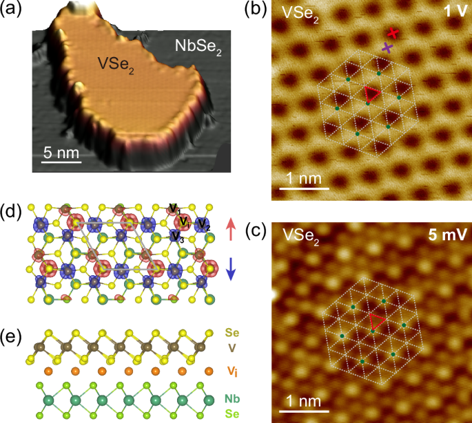
VSe2 with uniform \(\sqrt{3}\times \sqrt{3}\) phase was achieved for the first time. Figure 1a, b shows the STM morphology of the monolayer VSe2. Its atomic resolution image acquired at 5 mV
resolves the triangular lattice of the top layer Se (Fig. 1c, white dashed lines). The measured in-plane lattice constant of 0.35 nm and the monolayer height of ~0.60 nm both conform to
those of the 1T-VSe241,42. The atomic resolution image also features an evident \(\sqrt{3}\times \sqrt{3}\) superstructure, where one (Fig. 1c, green dot) of every three Se atoms (Fig. 1c,
red triangle) becomes brighter than the other two. The STM morphology of the \(\sqrt{3}\times \sqrt{3}\) superstructure drastically changes with bias, which appears as a honeycomb at 1 V
(Figs. 1b, S6), demonstrating its distinct electronic property. Typical tunneling spectra of the VSe2 indicate an evident gap of ~155 meV spanning the Fermi surface with gap edges locating
at about −130 mV and 25 mV, respectively (Fig. 2a). Those spectroscopic intensities spatially vary (Fig. S4), where the d_I_/d_V_ mappings drastically evolve with bias (Figs. 2b–g and S7).
Specifically, each unit of the \(\sqrt{3}\times \sqrt{3}\) pattern contains a Se atomic trimer of similar intensity (red triangle) at the bias range of about [−0.3 V, −0.1 V] (Fig. 2c). One
atom of the Se trimer appears brighter than the other two atoms at low bias of [−0.05 V, 0.3 V] (Fig. 2d, e), but becomes darker below −0.4 V (Fig. 2b). This observation, in conjunction with
the growth kinetics and DFT-calculations shown later, suggests the existence of intercalated V atoms in the heterostructure interface (Supplementary Note 1). On the other hand, as shown in
Fig. S5, spatial intensities at the two spectral gap edges show a clear anti-phase relationship, which is reminiscent of the CDW phase43. Next, we scrutinize the fine spectroscopic features
around _E_F to investigate the low energy excitations. Intriguingly, a pronounced sharp resonance surpassing _E_F emerges, which is peaked at 3 meV and superimposed on a broad peak that is
centered at about 25 meV (Fig. 3a, black curve). Its narrow peak width suggests it cannot be from conventional electronic state, but is relevant to many-body spin excitation and the most
probable origin is the Kondo resonance44,45. As such, we fitted the spectrum with a Fano line shape with a linear background \(\frac{{dI}(V)}{{dV}}=A\frac{{(q+\varepsilon
)}^{2}}{1+{\varepsilon }^{2}}+B\), where \(\varepsilon=\frac{({eV}-{\varepsilon }_{0})}{\varGamma }\), \(B=a \cdot V+b\) with the Fano factor _q_, the Kondo resonance energy \({\varepsilon
}_{0}\), and the intrinsic Kondo resonance width _Γ_. The fitting nicely matches the experimental spectrum, which gives a Kondo peak width _Γ_ of 3.9 meV and a Fano factor _q_ of 6 (Fig. 3a,
red curve]. In addition, the spectra of islands with different sizes exhibit same Kondo peaks (Fig. S22), ruling out the influence of quantum size effects. The Kondo resonance is further
justified from its temperature and magnetic field evolutions. A rigorous evidence for the Kondo resonance is its temperature evolution. The resonance broadens rapidly with increasing
temperature (Fig. 3a, black curves). Fano fittings to the spectra at different temperatures (Fig. 3a, red curves) extract the intrinsic _Γ_ (Fig. 3b, black dots) after subtracting the
influences from the thermal broadening and the lock-in modulation46. The relation of _Γ_ as a function of temperature _T_ can be excellently fitted using the well-established expression for
Kondo systems45,46,47, i.e. \(2\varGamma \left({{\rm{T}}}\right)=\sqrt{{(\alpha {k}_{B}T)}^{2}+{(2{k}_{B}{T}_{k})}^{2}}\), which yields a Kondo temperature \({T}_{k}\) ~ 44 K at \(\alpha\) =
5.1 (Fig. 3b). Moreover, upon applying magnetic field at 0.6 K, the resonance becomes suppressed with decreased peak height and increased peak width (Fig. 3c), conforming to the expected
behavior of a Kondo resonance. A Kondo peak splitting is not observed even under 12 T due to the large peak width. Spatial distribution of the Kondo resonance is measured with conductance
mapping at 5 mV (Fig. 2g), corresponding to the energy of the Kondo state. As the Kondo resonance is superimposed on the spectral background from the CDW pattern, which introduces a
periodically modulated electron density pattern in real space. As a result, the Kondo peak intensities from direct spectroscopic measurements also exhibit the same spatial pattern as the
CDW. Each CDW unit presumably hosts a localized magnetic moment in a similar fashion as the star of David motifs in 1T-TaS221, forming a spin matrix that interacts with itinerant electrons.
Line spectra surpassing multiple units of the \(\sqrt{3}\times \sqrt{3}\) pattern show that the Kondo resonance prevails over the entire surface (Fig. 3e). The fitted Kondo resonance widths
and Kondo amplitudes along the line are reasonably uniform, demonstrating the global nature of the Kondo lattice with the establishment of coherent Kondo screening48. To more clearly show
the spatial homogeneity of the normalized Kondo resonance, we selected all the spectra from the 2D conductance plot of Fig. 3e within a single CDW period as a typical example, and displayed
them in Fig. S8. The formation of the coherent Kondo lattice can also be manifested from the evolution of the Kondo resonance close to the island edge. In a coherent nano-scale Kondo
lattice, magnetic atoms at the inner and edge of the lattice have different quantum interference environments, resulting in a significant change in their Kondo resonances49. In our monolayer
VSe2 island, the Kondo resonance inside the island is uniform, but becomes gradually suppressed upon approaching the island edge (Fig. S19d, g), conforming to the coherent Kondo lattice
behavior. Note that Kondo lattice hallmarks a hybridization gap, which however is undetected in many Kondo lattice systems19,22. This is because its tunneling spectrum is determined by two
interfering tunneling paths from the STM tip between the itinerant electrons and the Kondo resonance (Supplementary Note 2). To manifest the hybridization gap, one needs to tune the
tunneling ratio between the two interfering tunneling paths. Since the lattice constants of VSe2 (0.352 nm) and the NbSe2 substrate (0.345 nm) are slightly different, larger VSe2 islands
could accumulate internal strain, whose local variations might potentially tune the tunneling ratio. Fig. S10a shows a typical large VSe2 island whose area size (462 nm2) is about twice
larger than that of Fig. 1a (292 nm2). Indeed, tunneling spectra acquired along a line at interior of the VSe2 island indicate prominent variations (Fig. S10c). Some of the spectra exhibit a
single Kondo peak (purple curve as a typical example, Fig. S10c, e), which is the same as that of Fig. 3. Importantly, most of the spectra clearly display a pair of split Kondo peaks [red
curve as a typical example, Fig. S10c, e), which hallmark the hybridization gap, in nice agreement with the hybridization gap reported in previous studies4,50. These two types of low-energy
excitation spectral shapes have been reproduced by the co-tunneling model with different tunneling ratios in Fig. S9b, c. Such hybridization gaps have been robustly observed in different
VSe2 islands in different batch of samples, as shown in Fig. S11 for another two examples. Those observations firmly confirm the presence of the hybridization gap in our system, providing
the clear-cut fingerprint of the coherent Kondo lattice. Strictly speaking, the co-tunneling model should be applied to fit the Kondo lattice spectrum and its temperature evolution. However,
it contains many parameters and does not possess a simple analytical expression, making such fitting to the experimental spectrum less straightforward. Thus, in actual Kondo lattice
material systems, the spectrum for single ion Kondo state is frequently used to fit the Kondo lattice spectrum for simplicity17,18,19,20. To unveil the experimental observations, we
performed the DFT calculations. Although a controversy exists about the intrinsic ferromagnetism in monolayer VSe251,52, it is believed that CDW formation would cancel magnetism53. Hence,
the existence of magnetic moment in the \(\sqrt{3}\times \sqrt{3}\) VSe2 is unexpected. We have constructed a series of possible VSe2/NbSe2 heterostructures to capture the experimental
features, with/without the inclusion of intercalated vanadium (Vi). We have searched for many different stacking orders (Fig. S12) and found that the structure shown in Fig. 1d, e fits best
to the experimental d_I_/d_V_ maps, while other constructed structures show noticeable derivations (Fig. S12). The calculated local density of states (DOS) based on that structure also
reasonably agrees with the experimental spectra (Fig. 2a). This gives an additional proof of the intercalated V atoms (Fig. S13). The intercalated V atoms profoundly influence the lattice
and electronic structures of this system, as shown in Fig. S3. Although \(\sqrt{3}\times \sqrt{3}\) CDWs are generally observed despite stacking order or intercalation, these CDW patterns
are characterized by V anti-trimerization with C3 symmetry, resulting in two inequivalent V-V bonds ~3.7 Å and ~3.3 Å. The symmetry is same as monolayer, suggesting CDWs in vdW
heterostructure are less influenced by interlayer interaction, as is also reflected in the electronic properties (Fig. S14b). However, the introduction of Vi under isosceles triangle V
(formed by two bonds of 3.3 Å and one of 3.7 Å) in the vdW heterostructure would result in all V-V bonds unequal with obvious C1 symmetry, e.g., V1-V2 ~ 3.7 Å V1-V3 ~ 3.0 Å and V2-V3 ~ 3.2 Å
(Fig. 1d). The electronic properties are also strongly influenced by Vi (Fig. S14c). Significant hybridizations can be found between Vi and VSe2/NbSe2 in the spin-up channel. Furthermore,
amounts of charges transfer from Vi into both VSe2 and NbSe2 layers, which could be responsible for the reduction of the observed layer height. This new CDW system possesses local magnetic
moments inside the superlattice. As can be seen in the calculated spin density distribution (Fig. 1d). Within one unit cell of the CDW phase magnetic moment of Vi is as large as ~1\({\mu
}_{B}\) composed of mixing \({3d}_{{xy}}\) and \({3d}_{{z}^{2}}\) at the energy range −0.9 ~ −0.55 eV below _E_F (Fig. S15), while the magnetic moment inside the VSe2 layer is ~ −0.9\({\mu
}_{B}\) mainly contributed by V2 (~ −0.7\({\mu }_{B}\) composed of \({3d}_{{yz}}\) and \({3d}_{{z}^{2}}\) at the energy range −0.75 ~ −0.3 eV below _E_F (Fig. S15)), opposite to Vi.
Importantly, the existence of Vi has also noticeably suppressed the magnetic exchange interaction between superlattice. Specifically, without Vi the calculated magnetic moments of the
monolayer \(\sqrt{3}\times \sqrt{3}\) VSe2 are ~ 3.3 \({\mu }_{B}\) (Fig. S14a), resulting in a relatively large ferromagnetic exchange interaction ~ 4 meV for nearest-neighboring unit cell.
However, with Vi the magnetic moments decrease to ~ 0.9 \({\mu }_{B}\) partially caused by the electrons transferring from Vi to the unoccupied \({3d}_{{z}^{2}}\) orbitals (Fig. S14c) and
the exchange interaction between superlattice is reduced to ~ 1 meV, destabilizing the long-range magnetic order and benefiting superconducting proximity effect. Overall, the magnetic moment
array, an ingredient for Kondo lattice, could be contributed by both VSe2 and Vi, but Vi is likely play a more important role as a result of flatter band dispersion (350 meV) and magnetic
moments closer to ~ 1\({\mu }_{B}\) than the V in VSe2 layer. Although the orbital bands forming the local moments are conventionally far from the Fermi level, they can be screened by the
itinerant conduction electrons via spin-flip scattering, which involves a virtual hopping process as in the case of Mn3Sn19. Overall, the CDW phase triggered by the intercalated vanadium
plays a vital role in the formation of Kondo lattice, indirectly influencing the interplay between the Kondo lattice and the proximity superconductivity. Having identified the Kondo lattice,
we study its interaction with the superconductivity of the NbSe2 substrate. For single Kondo impurity, its exchange interaction with Cooper pairs induces Yu-Shiba-Rusinov (YSR) bound states
inside the SC gap. While YSR states from single Kondo impurities have been extensively studied, the fate of Kondo lattice interacting with superconductivity remains unexplored in
experiment. As such, we performed spectroscopic measurement to the SC gap at 0.6 K. As is seen in Fig. 4(a, b), the measured d_I_/d_V_ spectra on the substrate and the VSe2 both show SC
gaps. With increasing temperature, SC gap of the substrate becomes gradually suppressed and disappears completely at 7 K. Interestingly, while the SC gap size of VSe2 is smaller than that of
the substrate, its gap follows a similar evolution trend as the substrate with an identical SC transition temperature, demonstrating the SC gap of VSe2 originates from the SC proximity
effect of the substrate. The superconducting proximity decay length of our intercalated VSe2 film is estimated as 2.1 ~ 3.1 nm by an exponential fitting to the superconducting gap sizes of
bare NbSe2 and monolayer VSe2 (Fig. S16), which is larger than the VSe2 films without intercalation54. In addition, the proximitized SC gap measured across multiple CDW periods is spatially
uniform (Fig. S17). In the presence of an adsorbate whose species is currently unknown, the Kondo peak is locally suppressed, but the SC gap is kept unchanged, conforming to the proximity
effect origin of the SC gap (Fig. S18) and substantiating the Kondo lattice formation, ruling out the presence of YSR states (Supplementary Note 3). Finally, we evaluated the spectral shape
of the proximitized SC gap. The SC gap of NbSe2 fully opens, whose spectral shape fits nicely to the BCS function, yielding a SC gap size of 1.07 meV (Fig. 4c). The measured gap size is
slightly smaller than that of the pristine NbSe2, 1.20 meV, which is likely caused by the growth of VSe2. The gap of the monolayer VSe2, on the other hand, exhibits finite DOS within the gap
and a pair of coherence peaks with higher intensity on the empty state (Fig. 4c, d). The asymmetric SC gap comes from the background introduced from the Kondo peak, which can be subtracted
to restore the gap symmetry (Fig. S20). Notably, the SC gap of VSe2 exhibits obviously more enhanced coherence peaks than the conventional BCS function, implying prominent entanglement
between superconductivity and the heavy electrons. To understand its unusual SC gap shape, we consider an effective Kondo lattice model in the \(\sqrt{3}\times \sqrt{3}\) CDW phase of the
monolayer VSe2, whose details are described in Methods. Here we summarize the key results in Fig.4e, f. In the normal state, the Kondo hybridization between local moments and itinerant
electrons gives rise to a heavy electron band crossing _E_F, characterized by the sharp resonance peak in the density of state near _E_F. A hybridization gap in the density of states opens
near _E_F. But the real system contains multiple conduction bands crossing _E_F, and therefore, in reality this gap is filled by other conduction bands that do not hybridize with local
moments for symmetry reason. In our model, the SC gap \({\Delta }_{0}\) of the neighboring NbSe2 layer acts as an effective SC pairing potential and induces a SC gap \(\Delta\)<Δ0 in the
VSe2 layer. The reduction of the SC gap is a direct consequence of strong competition between the superconductivity and Kondo hybridization, given both of them rely on formation of spin
singlet pairs. The pairing state consists of electrons in the heavy electron band that participate in superconductivity when the temperature is below the SC transition temperature and make
an additional contribution to the spectral weights. The hybridized nature of this band causes enhanced spectral weight of the coherence peak in the Kondo lattice model that deviates from the
function of a simple one-band BCS superconductor. DISCUSSION In summary, we achieved growth of monolayer VSe2 on superconducting 2H-NbSe2 substrate. The monolayer VSe2 exhibits a new
\(\sqrt{3}\times \sqrt{3}\) CDW phase and more importantly forms a coherent Kondo lattice with an identical periodicity as the CDW pattern. Superconductivity is established in the Kondo
lattice through proximity effect from the substrate. The proximitized SC gap exhibits more enhanced coherence peaks, whose spectral shape deviates from the function of one-band BCS
superconductor, but is reproduced by model calculations with heavy electrons participating the pairing condensate. Our work realizes a new van der Waals heterojunction system exhibiting
Kondo lattice behavior and coexisting proximitized superconductivity, which indicates that electrons from the coherent Kondo screening can take part in superconducting pairing. This could
facilitate the understanding of the unconventional superconductivity in heavy fermion systems, wherein exchange interactions among electrons of Kondo screening are believed essential55.
METHODS SAMPLE PREPARATION The bulk 2H-NbSe2 substrate was cleaved and further degassed at 450 °C and in an ultra-high vacuum chamber. After cleaving, the VSe2 films are grown by
co-deposition of high-purity Se (purity 99.999%) and V (purity 99.95%) atoms from a Knudsen cell and an electron-beam evaporator, respectively, while the 2H-NbSe2 substrate is kept at a
suitable temperature for 15 minutes. Different substrate temperatures (310°C ~ 435°C) correspond to different V-Se compounds. The temperature required for the \(\sqrt{3}\times \sqrt{3}\)
VSe2, which is the focus of this study, is slightly higher than 400 °C. STM MEASUREMENT The experiments are performed with a custom-made Unisoku STM (1300). An electrochemically etched W
wire is used as the STM tip. Prior to measurements, the tip is characterized on a Ag (111) multilayer film grown on a Si (111) substrate, which has been cleaned by several cycles of flashing
to 1500 K. The tunneling spectra are measured using a standard lock-in detection technique with a modulation voltage at 983 Hz. DFT CALCULATION Our first-principles calculations are
performed with Vienna ab initio simulation package (VASP)35 where projector augmented wave method is adopted56. The exchange-correlation term is treated with the Perdew-Burke-Ernzerhof (PBE)
form of the generalized gradient approximation57. The 3_p_63_d_44_s_1, 4_p_64_d_45_s_1 and the 4_s_24_p_4 electrons are treated as valence electrons for V, Nb and Se, respectively. We
construct a two-layer VSe2/NbSe2 heterojunction in our DFT calculation, which can capture the major characters of experimental monolayer-VSe2/bulk-NbSe2 structure. A vacuum layer of about 15
Å is added to avoid interactions between periodical layers and DFT-D3 method of Grimme with zero-damping function58 is adopted to correct the van der Waals force. Gaussian smearing of 0.05
eV is used in our calculations. Energy cutoff of 500 eV and _k_ mesh of \(8\times 8\times 1\) in Brillouin zone (BZ) are adopt for structural relaxation of the heterojunction, with force on
each atom is less than 0.005 eV/Å and the convergence criterion of total energy being 10-6 eV. Increased _k_ mesh of \(12\times 12\times 1\) in BZ and convergence criterion of total energy
10-7 eV are adopted in static calculations. We determine the intercalation structure by investigating the simulated d_I_/d_V_ maps with experiments. The simulation of d_I_/d_V_ maps is based
on the summation of DOS at corresponding energy _E_b within range \({E}_{b}\pm 0.01\) eV and a distance of about 3 Å from the surface. The effect of spin orbital coupling (SOC) is
negligible in our system and not considered. THEORETICAL MODEL The interplay of Kondo hybridization and proximitized superconductivity has been investigated by a Kondo lattice model within a
self-consistent mean-field approach. In principle, the CDW order leads to a multi-band electronic structure. A band close to half-filling may experience stronger electron correlations and
becomes localized, via an orbital-selective mechanism. Electrons in this localized band can then be approximated as local magnetic moments because charge excitations are heavily suppressed
and gapped. On the other hand, electrons in other bands are still itinerant. To understand the low-energy physics of this system consisting of both itinerant and localized electrons, here we
consider an effective Kondo lattice model defined on the \(\sqrt{3}\times \sqrt{3}\) triangular superlattice, which corresponds to the lattice structure of the \(\sqrt{3}\times \sqrt{3}\)
CDW phase of the monolayer VSe2. The Hamiltonian of the model reads as $$H=t{\sum}_{\left\langle i,j\right\rangle,\sigma }{c}_{i{\sigma }}^{{\dagger} }{c}_{j\sigma
}+\frac{J}{2}{\sum}_{i,\sigma,{\sigma }^{{\prime} }}{{{\boldsymbol{S}}}}_{i}\cdot {c}_{i\sigma }^{{\dagger} }{{{\boldsymbol{\tau }}}}_{\sigma {\sigma }^{{\prime} }}{c}_{i\sigma }-{\Delta
}_{0}{\sum}_{k}\left({c}_{k\uparrow }^{{\dagger} }{c}_{-k\downarrow }^{{\dagger} }+h.c.\right)$$ where \({c}_{i\sigma }^{{\dagger} }\) creates an electron of spin \(\sigma\) at the
superlattice site _i_ in the itinerant band, \({{{\boldsymbol{S}}}}_{i}\) denotes the \(S=1/2\) local magnetic moment induced in the CDW phase, \({{\boldsymbol{\tau }}}\) is the Pauli
matrix, \(t\) refers to the nearest neighbor hopping between itinerant electrons, and \(J\) is the Kondo coupling. Note that our purpose is to capture the essential physics of the Kondo
lattice. Therefore, we consider a single conduction band relevant to the Kondo hybridization, which can be approximately described by a tight-binding model with the nearest neighbor hopping.
The realistic electronic structure of the monolayer VSe2 may be more complicated, which can be described by including other conduction bands and with further neighboring terms. We assume
the SC gap in the NbSe2 layers is \({\Delta }_{0}\). This conventional BCS type gap acts as an attractive SC pairing potential to itinerant electrons in the monolayer VSe2 via the proximity
effect. To understand the interplay of Kondo hybridization and superconductivity in this model, we first rewrite the local spin operator in the pseudo-fermion representation:
\({{{\boldsymbol{S}}}}_{i}=\frac{1}{2}{f}_{i\sigma }^{{\dagger} }{{{\boldsymbol{\tau }}}}_{\sigma {\sigma }^{{\prime} }}{f}_{i{\sigma }}\), where \({f}_{i\sigma }\) satisfies the fermionic
commutation. For an exact representation of the \(S=1/2\) local moment, we employ a constraint \({\sum }_{\sigma }{f}_{i\sigma }^{{\dagger} }{f}_{i\sigma }=1\) via introducing a Lagrange
multiplier \({\epsilon }_{f}\) in the Hamiltonian. In the pseudo-fermion representation, the local moment corresponds to a flat pseudo-fermion band at the Fermi energy. To handle the Kondo
coupling term, we then adopt a mean-field decomposition $${\sum}_{i,\sigma,{\sigma }^{{\prime} }}{{{\boldsymbol{S}}}}_{i}\cdot {c}_{i\sigma }^{{\dagger} }{{{\boldsymbol{\tau }}}}_{\sigma
{\sigma }^{{\prime} }}{c}_{i\sigma }\approx V{\sum}_{i,\sigma }{c}_{i,\sigma }^{{\dagger} }{f}_{i\sigma }$$ where \(V=\langle {f}_{i,\sigma }^{{\dagger} }{c}_{i\sigma }\rangle\),
parametrizes the Kondo hybridization. For simplicity, we assume translational symmetry of \(V\). In our calculation, \(V\) and \({\epsilon }_{f}\) are determined in a self-consistent way.
Given the bilinear coupling between _c_ and _f_ fermions, it is expected that the SC pairing between itinerant electrons can induce pairing within the pseudo-fermions. We therefore introduce
an additional mean field \({\Delta }_{f}=\langle {f}_{k\uparrow }{f}_{-k\downarrow }\rangle\), which is self-consistently determined together with \(V\) and \({\epsilon }_{f}\). In the
normal state, we can set \({\Delta }_{0}=0\). Our results of the band structure and the corresponding density of states projected to the conduction electrons at \(t=1,J=5.5\) are shown in
Fig. 4e of the main text. It is clear that the Kondo coupling causes a finite hybridization between the itinerant and pseudo fermions. As a consequence of the Kondo hybridization, the flat
pseudo-fermion band becomes weakly dispersive, forming a heavy electron band. This heavy electron band is characterized by a sharp resonance peak of the density of states near the Fermi
energy. This Kondo resonance peak is also resolved in experiment. A rough estimate from the CDW gap gives _t_ ~ 50 meV. With this, our calculation suggests that the heavy band should be very
close to the Fermi level at ~10 meV. The energy of the heavy band is in reasonable agreement with the experimentally observed Kondo resonance at around 5 meV. Note that in our model a
finite hybridization gap opens below the Fermi energy. In reality, such a hybridization gap is likely not observed because the gap could be filled by other conduction bands across the Fermi
energy that does not hybridize with local moments for symmetry reasons. When \({\Delta }_{0}\) is turned on, the model can be solved via a Bogoliubov transformation. As discussed above, in
the presence of Kondo hybridization this is an effective two-band system, and the excitation energies in the SC state are \({E}_{k}^{\pm }\). The induced SC gap \(\Delta\) can be calculated
from the lowest quasiparticle excitation energy \({E}_{k}^{-}\) at the Fermi energy, e.g., \(\Delta={E}_{k={k}_{F}}^{-}\). The density of states can be obtained from \(\rho={\sum
}_{k,\alpha=\pm }[\delta (\omega -{E}_{k}^{\alpha })+\delta (\omega+{E}_{k}^{\alpha })]\). The calculated density of states near the Fermi energy (set to zero) in the Kondo lattice at
\({\Delta }_{0}=0.1,t=1,J=5.5\) is plotted in Fig. 4f of the main text. Compared to that of a one-band superconductor with SC gap \({\Delta }_{0}\), we find two major differences. First, the
induced SC gap \(\Delta\) in the Kondo lattice is smaller than \({\Delta }_{0}\). The reduction of the SC gap is understood as follows: An itinerant electron may either participate in
superconductivity by forming a spin singlet Cooper pair with another itinerant electron, or screen the local moment by forming a Kondo singlet. These two processes are in direct competition.
As a result, the SC gap is reduced in the presence of Kondo hybridization. The other difference is that the spectral weight of the coherence peak is enhanced in the Kondo lattice model
compared to that in a simple BCS superconductor. Note that the band near the Fermi energy is the heavy electron band. This heavy electron band contains a significant portion of _f_-fermions.
The participation of these electrons to superconductivity naturally causes enhancement of spectral weight. Moreover, as mentioned above, the Kondo lattice can be viewed as a two-band system
consisting of _c_- and _f_-fermions. Therefore, the gap function is more complicated than and can deviate from that of a simple one-band superconductor. DATA AVAILABILITY The data that
support the findings of this study are available from the corresponding author upon request. CODE AVAILABILITY The code that supports the findings of this study is available from the
corresponding author upon request. REFERENCES * Morr, D. K. Theory of scanning tunneling spectroscopy: From Kondo impurities to heavy fermion materials. _Rep. Prog. Phys._ 80, 014502 (2017).
Article ADS PubMed Google Scholar * Stewart, G. R. Heavy-fermion systems. _Rev. Mod. Phys._ 56, 755–787 (1984). Article ADS CAS Google Scholar * Yazdani, A., da Silva Neto, E. H.
& Aynajian, P. Spectroscopic imaging of strongly correlated electronic states. _Annu. Rev. Condens. Matter Phys._ 7, 11–33 (2016). Article ADS Google Scholar * Aynajian, P. et al.
Visualizing heavy fermions emerging in a quantum critical Kondo lattice. _Nature_ 486, 201–206 (2012). Article ADS CAS PubMed Google Scholar * Neumann, M., Nyéki, J., Cowan, B. &
Saunders, J. Bilayer 3He: A Simple Two-Dimensional Heavy-Fermion System with Quantum Criticality. _Science_ 317, 5843 (2007). Article Google Scholar * Gegenwart, P., Si, Q. & Steglich,
F. Quantum criticality in heavy-fermion metals. _Nat. Phys._ 4, 186–197 (2008). Article CAS Google Scholar * Stockert, O. & Steglich, F. Unconventional Quantum Criticality in
Heavy-Fermion Compounds. _Annu. Rev. Condens. Matter Phys._ 2, 79 (2011). Article ADS CAS Google Scholar * Si, Q. & Steglich, F. Heavy fermions and quantum phase transitions.
_Science_ 329, 1161 (2010). Article ADS CAS PubMed Google Scholar * Maple, M. B. et al. Non fermi liquid ground states in strongly correlated f-electron materials. _J. Low Temp. Phys._
99, 223–249 (1995). Article ADS CAS Google Scholar * Stewart, G. R. Non-Fermi-liquid behavior in d- and f-electron metals. _Rev. Mod. Phys._ 73, 797–855 (2001). Article ADS CAS Google
Scholar * Löhneysen, H. V., Rosch, A., Vojta, M. & Wölfle, P. Fermi-liquid instabilities at magnetic quantum phase transitions. _Rev. Mod. Phys._ 79, 1015–1075 (2007). Article ADS
Google Scholar * Seiro, S. et al. Evolution of the Kondo lattice and non-Fermi liquid excitations in a heavy-fermion metal. _Nat. Commun._ 9, 3324 (2018). Article ADS CAS PubMed PubMed
Central Google Scholar * Pfleiderer, C. Superconducting phases of f-electron compounds. _Rev. Mod. Phys._ 81, 1551–1624 (2009). Article ADS CAS Google Scholar * Allan, M. P. et al.
Imaging Cooper pairing of heavy fermions in CeCoIn5. _Nat. Phys._ 9, 468–473 (2013). Article CAS Google Scholar * Zhou, B. B. et al. Visualizing nodal heavy fermion superconductivity in
CeCoIn5. _Nat. Phys._ 9, 474–479 (2013). Article CAS Google Scholar * Jiao, L. et al. Chiral superconductivity in heavy-fermion metal UTe2. _Nature_ 579, 523–527 (2020). Article ADS CAS
PubMed Google Scholar * Jiang, Y., Zhang, Y. N., Cao, J. X., Wu, R. Q. & Ho, W. Real-space imaging of Kondo screening in a two-dimensional O2 lattice. _Science_ 333, 6040 (2011).
Article Google Scholar * Zhang, Y. et al. Emergence of Kondo lattice behavior in a van der Waals itinerant ferromagnet, Fe3GeTe2. _Sci. Adv._ 4, eaao6791 (2018). Article ADS PubMed
PubMed Central Google Scholar * Zhang, S. S. et al. Many-Body Resonance in a Correlated Topological Kagome Antiferromagnet. _Phys. Rev. Lett._ 125, 046401 (2020). Article ADS CAS PubMed
Google Scholar * Vaňo, V. et al. Artificial heavy fermions in a van der Waals heterostructure. _Nature_ 599, 582–586 (2021). Article ADS PubMed Google Scholar * Ruan, W. et al.
Evidence for quantum spin liquid behaviour in single-layer 1T-TaSe2 from scanning tunnelling microscopy. _Nat. Phys._ 17, 1154 (2021). Article CAS Google Scholar * Shen, S. et al.
Inducing and tuning Kondo screening in a narrow-electronic-band system. _Nat. Commun._ 13, 2156 (2022). Article ADS CAS PubMed PubMed Central Google Scholar * Geim, A. K. &
Grigorieva, I. V. Van der Waals heterostructures. _Nature_ 499, 419–425 (2013). Article CAS PubMed Google Scholar * Liu, Y. et al. Van der Waals heterostructures and devices. _Nat. Rev.
Mater._ 1, 16042 (2016). Article ADS CAS Google Scholar * Novoselov, K. S., Mishchenko, A., Carvalho, A. & Castro Neto, A. H. 2D materials and van der Waals heterostructures.
_Science_ 353, 9439 (2016). Article Google Scholar * Kezilebieke, S. et al. Topological superconductivity in a van der Waals heterostructure. _Nature_ 588, 424–428 (2020). Article ADS
CAS PubMed Google Scholar * Bodensiek, O., Pruschke, T. & Zitko, R. Superconductivity in the Kondo lattice model. _J. Phys. Conf. Ser._ 200, 012162 (2010). Article Google Scholar *
Koga, A. & Werner, P. Superfluid State in the Periodic Anderson Model with Attractive Interactions. _J. Phys. Soc. Jpn._ 79, 114401 (2010). Article ADS Google Scholar * Pokorný, V.
& Ram, P. Evolution of the Andreev bands in the half-filled superconducting periodic Anderson model. _Phys. Rev. B_ 104, 155102 (2021). Article ADS Google Scholar * Sousa, S. D., de
Lima, J. P., Costa, N. C. & dos Santos, R. R. Superconducting Kondo phase in an orbitally separated bilayer. _Phys. Rev. Res._ 2, 033168 (2020). Article Google Scholar * Bardeen, J.,
Cooper, L. N. & Schrieffer, J. R. Theory of Superconductivity. _Phys. Rev._ 108, 1175 (1957). Article ADS MathSciNet CAS Google Scholar * Dynes, R. C., Narayanamurti, V. &
Garno, J. P. Direct Measurement of Quasiparticle-Lifetime Broadening in a Strong-Coupled Superconductor. _Phy. Rev. Lett._ 41, 1509 (1978). Article ADS CAS Google Scholar * Herman, F.
& Hlubina, R. Microscopic interpretation of the Dynes formula for the tunneling density of states. _Phys. Rev. B_ 94, 144508 (2016). Article ADS Google Scholar * Yang, X. et al.
Possible Phason-Polaron Effect on Purely One-Dimensional Charge Order of Mo6Se6 Nanowires. _Phys. Rev. X_ 10, 031061 (2020). CAS Google Scholar * Kresse, G. & Furthmüller, J. Efficient
iterative schemes for ab initio total-energy calculations using a plane-wave basis set. _Phys. Rev. B_ 54, 11169 (1996). Article ADS CAS Google Scholar * Oh, S. et al. Synthesis of a
one-dimensional atomic crystal of vanadium selenide (V2Se9). _RSC Adv._ 8, 33980 (2018). Article ADS CAS PubMed PubMed Central Google Scholar * Chae, S. et al. Isolation of inorganic
molecular chains from rodlike bulk V2Se9 crystal by liquid exfoliation. _RSC Adv._ 8, 35348 (2018). Article ADS CAS PubMed PubMed Central Google Scholar * Wong, P. K. J. et al.
Evidence of Spin Frustration in a Vanadium Diselenide Monolayer Magnet. _Adv. Mater._ 31, 1901185 (2019). Article Google Scholar * Feng, J. G. et al. Electronic Structure and Enhanced
Charge-Density Wave Order of Monolayer VSe2. _Nano Lett._ 18, 4493–4499 (2018). Article ADS CAS PubMed Google Scholar * Duvjir, G. et al. Emergence of a Metal−Insulator Transition and
High-Temperature Charge-Density Waves in VSe2 at the Monolayer Limit. _Nano Lett._ 18, 5432–5438 (2018). Article ADS CAS PubMed Google Scholar * Bayard, M. & Sienko, M. J. Anomalous
electrical and magnetic properties of vanadium diselenide. _J. Solid State Chem._ 19, 325–329 (1976). Article ADS CAS Google Scholar * Tsutsumi, K. X-ray-diffraction study of the
periodic lattice distortion associated with a charge-density wave in 1T-VSe2. _Phys. Rev. B_ 26, 5756 (1982). Article ADS CAS Google Scholar * Sacks, W., Roditchev, D. & Klein, J.
Voltage-dependent STM image of a charge density wave. _Phys. Rev. B_ 57, 13118 (1998). Article ADS CAS Google Scholar * Madhavan, V., Chen, W., Jamneala, T., Crommie, M. F. &
Wingreen, N. S. Tunneling into a Single Magnetic Atom: Spectroscopic Evidence of the Kondo Resonance. _Science_ 280, 567 (1998). Article ADS CAS PubMed Google Scholar * Ternes, M.,
Heinrich, A. J. & Schneider, W.-D. Spectroscopic manifestations of the kondo effect on single adatoms. _J. Phys. Condens. Matter_ 21, 053001 (2009). Article ADS PubMed Google Scholar
* Eickhoff, F. et al. Inelastic electron tunneling spectroscopy for probing strongly correlated many-body systems by scanning tunneling microscopy. _Phys. Rev. B_ 101, 125405 (2020).
Article ADS CAS Google Scholar * Lu, S. Z. et al. PTCDA Molecular Monolayer on Pb Thin Films: An Unusual π-Electron Kondo System and Its Interplay with a Quantum-Confined Superconductor.
_Phys. Rev. Lett._ 127, 186805 (2021). Article ADS CAS PubMed Google Scholar * Moro-Lagares, M. et al. Real space manifestations of coherent screening in atomic scale Kondo lattices.
_Nat. Commun._ 10, 2211 (2019). Article ADS CAS PubMed PubMed Central Google Scholar * Figgins, J. et al. Quantum engineered Kondo lattices. _Nat. Commun._ 10, 1038 (2019). Article
Google Scholar * Wan, W. et al. Evidence for ground state coherence in a two-dimensional Kondo lattice. _Nat. Commun._ 14, 7005 (2023). Article ADS CAS PubMed PubMed Central Google
Scholar * Bonilla, M. et al. Strong room-temperature ferromagnetism in VSe2 monolayers on van der Waals substrates. _Nat. Nanotechnol._ 13, 289 (2018). Article ADS CAS PubMed Google
Scholar * Yu, W. et al. Chemically exfoliated VSe2 monolayers with room‐temperature ferromagnetism. _Adv. Mater._ 31, 1903779 (2019). Article CAS Google Scholar * Fumega, A. O. et al.
Absence of ferromagnetism in VSe2 caused by its charge density wave phase. _J. Phys. Chem. C_ 123, 27802 (2019). Article CAS Google Scholar * Kezilebieke, S. et al. Electronic and
magnetic characterization of epitaxial VSe2 monolayers on superconducting NbSe2. _Commun. Phys._ 3, 116 (2020). Article CAS Google Scholar * Monthoux, P., Pines, D. & Lonzarich, G.
Superconductivity without phonons. _Nature_ 450, 1177–1183 (2007). Article ADS CAS PubMed Google Scholar * Blöchl, P. E. Projector augmented-wave method. _Phys. Rev. B_ 50, 17953–17979
(1994). Article ADS Google Scholar * Perdew, J. P., Burke, K. & Ernzerhof, M. Generalized gradient approximation made simple. _Phys. Rev. Lett._ 77, 3865–3868 (1996). Article ADS
CAS PubMed Google Scholar * Grimme, S., Antony, J., Ehrlich, S. & Krieg, H. A consistent and accurate ab initio parametrization of density functional dispersion correction (DFT-D) for
the 94 elements H-Pu. _J. Chem. Phys._ 132, 154104 (2010). Article ADS PubMed Google Scholar Download references ACKNOWLEDGEMENTS We thank Qimiao Si of Rice university, Feng Liu of Utah
university, Testuo Hanaguri of RIKEN, Yifeng Yang of Institute of physics, Chinese academy of sciences for discussions. This work was funded by the National Key Research and Development
Program of China (Grant Nos. 2022YFA1402400, 2018YFA0307000, 2021YFA1600201, 2022YFA1403203), the National Natural Science Foundation of China (Grant Nos. 92265201, U20A6002, 12088101,
12047508, 12174441, 12274412), the Joint Funds of the National Natural Science Foundation of China and the Chinese Academy of Sciences’ Large-Scale Scientific Facility (Grant Nos. U1932217
and U2032215) and NSAF under Grant No. U2230402. AUTHOR INFORMATION Author notes * These authors contributed equally: Kai Fan, Heng Jin, Bing Huang. AUTHORS AND AFFILIATIONS * School of
Physics and Wuhan National High Magnetic Field Center, Huazhong University of Science and Technology, Wuhan, 430074, China Kai Fan, Zhen-Yu Liu, Hui-Nan Xia, Li-Si Liu, Yao Zhang, Tao Xie,
Qiao-Yin Tang, Gang Chen, Wen-Hao Zhang & Ying-Shuang Fu * School of Physics and Astronomy, Beijing Normal University, Beijing, 100875, China Heng Jin & Bing Huang * Beijing
Computational Science Research Center, Beijing, 100093, China Heng Jin & Bing Huang * Department of Physics and Beijing Key Laboratory of Opto-electronic Functional Materials and
Micro-nano Devices, Renmin University of China, Beijing, 100872, China Guijing Duan & Rong Yu * Key Laboratory of Materials Physics, Institute of Solid State Physics, Chinese Academy of
Sciences, Hefei, 230031, China F. C. Chen, X. Luo, W. J. Lu & Y. P. Sun * High Magnetic Field Laboratory, Chinese Academy of Sciences, Hefei, 230031, China Y. P. Sun * Collaborative
Innovation Center of Advanced Microstructures, Nanjing University, Nanjing, 210093, China Y. P. Sun * Wuhan Institute of Quantum Technology, Wuhan, 430206, China Ying-Shuang Fu Authors * Kai
Fan View author publications You can also search for this author inPubMed Google Scholar * Heng Jin View author publications You can also search for this author inPubMed Google Scholar *
Bing Huang View author publications You can also search for this author inPubMed Google Scholar * Guijing Duan View author publications You can also search for this author inPubMed Google
Scholar * Rong Yu View author publications You can also search for this author inPubMed Google Scholar * Zhen-Yu Liu View author publications You can also search for this author inPubMed
Google Scholar * Hui-Nan Xia View author publications You can also search for this author inPubMed Google Scholar * Li-Si Liu View author publications You can also search for this author
inPubMed Google Scholar * Yao Zhang View author publications You can also search for this author inPubMed Google Scholar * Tao Xie View author publications You can also search for this
author inPubMed Google Scholar * Qiao-Yin Tang View author publications You can also search for this author inPubMed Google Scholar * Gang Chen View author publications You can also search
for this author inPubMed Google Scholar * Wen-Hao Zhang View author publications You can also search for this author inPubMed Google Scholar * F. C. Chen View author publications You can
also search for this author inPubMed Google Scholar * X. Luo View author publications You can also search for this author inPubMed Google Scholar * W. J. Lu View author publications You can
also search for this author inPubMed Google Scholar * Y. P. Sun View author publications You can also search for this author inPubMed Google Scholar * Ying-Shuang Fu View author publications
You can also search for this author inPubMed Google Scholar CONTRIBUTIONS Y.S.F. conceived the project. K.F. performed the experiments with the help of Z.Y. L., H.N. X., L.S. L., Y. Z., T.
X., Q.Y. T., G. C. and W.H.Z. H.J. and B.H. carried out the DFT calculations. G.J.D. and R.Y. carried out the effective Kondo lattice model calculations. F.C.C., X.L., W.J.L. and Y.P.S.
synthesized the NbSe2 crystals. K.F., Z.Y.L., Y.Z., H.J., B.H., G.J.D., R.Y., and Y.S.F. analyzed the data. Y.S.F., B.H., R.Y., K.F., H.J. and G.J.D. wrote the manuscript with comments from
all authors. Y.S.F. supervised the project. CORRESPONDING AUTHOR Correspondence to Ying-Shuang Fu. ETHICS DECLARATIONS COMPETING INTERESTS The authors declare no competing interests. PEER
REVIEW PEER REVIEW INFORMATION _Nature Communications_ thanks Han Woong Yeom, and the other, anonymous, reviewer(s) for their contribution to the peer review of this work. A peer review file
is available. ADDITIONAL INFORMATION PUBLISHER’S NOTE Springer Nature remains neutral with regard to jurisdictional claims in published maps and institutional affiliations. SUPPLEMENTARY
INFORMATION SUPPLEMENTARY INFORMATION PEER REVIEW FILE RIGHTS AND PERMISSIONS OPEN ACCESS This article is licensed under a Creative Commons Attribution 4.0 International License, which
permits use, sharing, adaptation, distribution and reproduction in any medium or format, as long as you give appropriate credit to the original author(s) and the source, provide a link to
the Creative Commons licence, and indicate if changes were made. The images or other third party material in this article are included in the article’s Creative Commons licence, unless
indicated otherwise in a credit line to the material. If material is not included in the article’s Creative Commons licence and your intended use is not permitted by statutory regulation or
exceeds the permitted use, you will need to obtain permission directly from the copyright holder. To view a copy of this licence, visit http://creativecommons.org/licenses/by/4.0/. Reprints
and permissions ABOUT THIS ARTICLE CITE THIS ARTICLE Fan, K., Jin, H., Huang, B. _et al._ Artificial superconducting Kondo lattice in a van der Waals heterostructure. _Nat Commun_ 15, 8797
(2024). https://doi.org/10.1038/s41467-024-53166-9 Download citation * Received: 13 August 2024 * Accepted: 02 October 2024 * Published: 11 October 2024 * DOI:
https://doi.org/10.1038/s41467-024-53166-9 SHARE THIS ARTICLE Anyone you share the following link with will be able to read this content: Get shareable link Sorry, a shareable link is not
currently available for this article. Copy to clipboard Provided by the Springer Nature SharedIt content-sharing initiative