- Select a language for the TTS:
- UK English Female
- UK English Male
- US English Female
- US English Male
- Australian Female
- Australian Male
- Language selected: (auto detect) - EN
Play all audios:
ABSTRACT The electrical control of the non-trivial topology in Weyl antiferromagnets is of great interest for the development of next-generation spintronic devices. Recent studies suggest
that the spin Hall effect can switch the topological antiferromagnetic order. However, the switching efficiency remains relatively low. Here, we demonstrate the effective manipulation of
antiferromagnetic order in the Weyl semimetal Mn3Sn using orbital torques originating from either metal Mn or oxide CuOx. Although Mn3Sn can convert orbital current to spin current on its
own, we find that inserting a heavy metal layer, such as Pt, of appropriate thickness can effectively reduce the critical switching current density by one order of magnitude. In addition, we
show that the memristor-like switching behaviour of Mn3Sn can mimic the potentiation and depression processes of a synapse with high linearity—which may be beneficial for constructing
accurate artificial neural networks. Our work paves a way for manipulating the topological antiferromagnetic order and may inspire more high-performance antiferromagnetic functional devices.
SIMILAR CONTENT BEING VIEWED BY OTHERS GIANT FIELD-LIKE TORQUE BY THE OUT-OF-PLANE MAGNETIC SPIN HALL EFFECT IN A TOPOLOGICAL ANTIFERROMAGNET Article Open access 18 November 2021
PERPENDICULAR FULL SWITCHING OF CHIRAL ANTIFERROMAGNETIC ORDER BY CURRENT Article 20 July 2022 OBSERVATION OF ANTI-DAMPING SPIN–ORBIT TORQUES GENERATED BY IN-PLANE AND OUT-OF-PLANE SPIN
POLARIZATIONS IN MNPD3 Article 03 April 2023 INTRODUCTION Topological materials have attracted intensive attentions due to their robust topologically protected states, many exotic properties
and promising applications for quantum computing and spintronics1,2. According to the dimensionality of electronic bands touching, the topological states of materials can be classified into
topological insulators3,4, Dirac semimetals5,6 and Weyl semimetals7,8, etc. Weyl semimetal has the feature of Weyl fermion with the presence of the chiral node (i.e. Weyl node) and the
Fermi arc surface states connecting the Weyl-node pair with opposite chirality9. The Weyl node is a linearly crossing point of two non-degenerate bands which requires breaking inversion
symmetry or time reversal symmetry. In order for developing electronic device, it is essential for effective electrical manipulation of the nontrivial topologic states e.g. Weyl nodes.
Magnetic Weyl semimetal is considered as an ideal material candidate since the time reversal symmetry is breaking and the location and enegy of Weyl nodes in the Brillouin zone depend on the
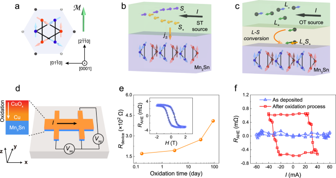
magnetization direction2. Mn3Sn is a typical Weyl semimetal and non-collinear antiferromagnet (AFM)10,11,12,13. As shown in Fig. 1a, the spin structure of Mn3Sn consists of two kagome
planes with opposite chirality. This hexagonal spin texture can be considered as a ferroic ordering of a cluster magnetic octupole _M_ and it breaks time reversal symmetry macroscopically.
AFMs have negligible stray field and ultra-fast magnetic dynamics, which helps to overcome the integrability and speed bottlenecks of traditional spintronic devices14,15,16,17. Furthermore,
all-AFM-based magnetic tunnel junctions (MTJ) with a sizable tunneling magnetoresistance (TMR) ratio have recently been demonstrated18,19. To date, researchers have demonstrated that spin
torques (ST) can manipulate the Weyl nodes in Mn3Sn or Co2MnGa manifested with the change in anormolous Hall effect (AHE)20,21,22,23,24, using a similar protocol as for heavy
metal/ferromagnets (HM/FM)25,26,27,28,29 where the spin current generated in heavy metal by spin Hall effect (SHE) is injected into FM and a torque is exerted on FM. As shown in Fig. 1b, the
generated spin current induced by current along <0001> direction can be directly exerted on the kagome planes of Mn3Sn and induce the magnetization switching. The switching efficiency
largely depends on the charge-current-to-spin-current conversion efficiency, i.e., the spin Hall angle (SHA), in the adjacent spin current source layer. To improve the efficiency and reduce
the switching current density _J_c, except for exploring novel materials with high SHA, it is also desirable to search alternative mechanisms to realize current-induced switching of
topological states with high energy efficiency. In this work, we propose to utilize orbital torques (OT) which originate from orbital Hall effect (OHE) or orbital Rashba-Edelstein effect
(OREE) to manipulate the magnetic order in topological AFM. The basic schematic is shown in Fig. 1c. An applied current along <0001> direction can induce orbital current in OT source
layer30,31,32. Before the generated orbital current can be exerted on the magnetization of Mn3Sn, it need to be converted to spin current by an additional spin-orbit coupling (SOC)33.
Compared with the limited SHA in spin current source material, it has been demonstrated that orbit current source materials possess a much higher orbit current generation efficiency34,35.
Therefore, the critical switching current density _J_c is expected to be effectively reduced. Herein, we successfully demonstrate OT-driven magnetization switching in Mn3Sn and prove that
the orbit-current-to-spin-current (L-S) conversion can be done either by Mn3Sn itself or by inserting a heavy metal with strong SOC. we have achieved _J_c as low as ~1 × 10¹⁰ A/m2, which is
more than one order of magnitude lower than the common _J_c in SHE-driven framework. Furthermore, we show that the stable memristor-like switching characteristics offers Mn3Sn with excellent
plasticity to mimic an artificial synapse with linear potentiation and depression processes, which is beneficial for constructing neural networks with high accuracy. RESULTS OT-DRIVEN
MAGNETIZATION SWITCHING IN TOPOLOGICAL MN3SN We deposited 40-nm-thick Mn3Sn film on thermally oxidized silicon substrates by magnetron sputtering (see details in Methods). By energy
dispersive spectrometry (EDS) mapping, the atomic percentage of MnSn alloy is determined to be around Mn(3.05-3.1)Sn. The x-ray diffraction (XRD) _θ_−2_θ_ scans results of the deposited
Mn3Sn is shown Supplementary Note 1. Compared with pure Si substrate, a clear Mn3Sn (0002) crystal peak is observed in the film sample. SQUID measurement indicates that our film exhibits a
tiny out-of-plane magnetization (see Supplementary Note 1). This tiny out-of-plane hysteresis loop suggests there exist crystalline grains with its kagome plane in the film normal since the
spin canting is in the (0001) kagome plane. We further carried out magneto-transport and anormolous Nerst effect (ANE) measurements to confirm the Weyl semimetal of our deposited Mn3Sn
films. Planar Hall effect (PHE) and in-plane angular magnetoresistance (AMR) are shown in Supplementary Figure 1c. The PHE and AMR follow the functions \({R}_{{xy}}=-\Delta R\sin \theta \cos
\theta\) and \({R}_{{xx}}={R}_{\perp }-\Delta R{\cos }^{2}\theta\), respectively, where \(\Delta R={R}_{\perp }-{R}_{\parallel }\), and \({R}_{\perp }\) and \({R}_{\parallel }\) are the
resistances when the magnetic field directions are perpendicular and parallel to the charge current direction, respectively. These are consistent with the feature of the chiral anomaly
induced PHE and AMR in Weyl semimetal9,20. Comparing to the effect of magnetization, ANE in Weyl semimetal is much enhanced due to the Weyl nodes around Fermi level11. The large ANE and
small magnetization further confirm that our Mn3Sn films are the Weyl semimetal (Supplementary Figure 1b and c). It has been widely demonstrated that OT can be observed in the naturally
oxidized Cu36,37. Thus, we firsly choose oxidized Cu to verify the impact of OT on the magnetization switching of Mn3Sn antiferromagnet. As shown in inset of Fig. 1d, we firstly deposited a
Cu layer on the Mn3Sn layer and then follow the method in previous works to naturally oxidize Cu at atmosphere for different time37. The films were fabricated into Hall bar device of 5 μm
width to implement magneto-transport measurement. The schematic setup of the measurement is illustrated in Fig. 1d. The longitudinal resistance shows a continuous increase with oxidation
time, which suggests the gradual oxidation of Cu layer with the time. We then measure the AHE resistance _R_AHE (inset in Fig. 1e) as a function of the out-of-plane magnetic field to
estimate the switchable magnetic domains which corresponds to the crystalline grains with Kogame plane in the film normal. In the absence of magnetic field, there exist two stable magnetic
states which correspond to the magnetic octupole _M_ along ± Z directions, respectively. We then carry out current-induced switching experiments (Fig. 1f). Since Cu is a light metal with
negligible SOC, current-induced magnetization switching is absent in the as-deposited Mn3Sn/Cu film. As a comparison, a deterministic magnetization switching loop, corresponding to a
switching ratio of ~ 25%, is well achieved in the device after natural oxidatization process of the Cu. We are also aware that several works reported current-induced switching in Mn3Sn
single layer with specific crystal configuration38,39. However, we didn’t observe any switching phenomenon in our deposited Mn3Sn single layer (Supplementary Note 2), verifying that the
magnetization switching driving force indeed comes from the achieved Cu/CuOx layer. Additionally, in Supplementary Note 3, we demonstrated that only when the applied FM like Ni exhibits a
high SOC, one can observe a sizable effective SHA in FM/Cu/CuOx heterostructure40. From one side, it verifies that the main switching driving force from Cu/CuOx is OTs instead of possible
STs. From the other side, it emphasizes again that the orbital current originated from CuOx must complete the _L-S_ conversion process shown in Fig. 1c to manipulate the magnetic dynamics in
FM. Our deterministic switching results in Mn3Sn/Cu/CuOx device directly prove that Mn3Sn itself can complete the _L-S_ conversion process like what Ni does and the spin current converted
from orbit current is then to switch the magnetization of Mn3Sn layer. More experimental evidences related to SOC and _L-S_ conversion in Mn3Sn will be presented in the next section. Note
that, for practical use, it is important to quantitatively control the orbital Hall angle in the device. In such case, metallic OT sources have an application edge over naturally oxidized
Cu. We thus employ an heterostructure composed of Mn3Sn (40 nm)/Pt(_t_Pt)/Mn(_t_Mn) trilayer (Fig. 2a) to further investigate the detailed OT-based manipulation characteristics of
topological magnetization. Mn is theoretically predicted to possess a large orbital Hall angle (~18)35. The inserted Pt layer serve as an additional _L_-_S_ conversion layer which helps to
gain more spin torques33,41. In a device where _t_Pt = 2 nm and _t_Mn = 10 nm, deterministic OT-driven magnetization switching in Mn3Sn is achieved as well (see detailed switching loops in
Supplementary Note 4). An external magnetic field _H_ex is required to break the in-plane symmetry during the switching process. When reversing the direction of _H_ex, the switching polarity
also changes. This switching characteristic is very similar to the SHE-induced switching protocol for FMs. Moreover, we have observed a _H_ex-dependent switching ratio trend in the sample.
The switching ratio is defined as Δ_R_c/Δ_R_H, where Δ_R_c and Δ_R_H are current-induced and field-induced change of _R_AHE. As shown in Fig. 2b, as the absolute value of _H_ex increases,
the switching ratio will first increase and then saturate when exceeds 2 kOe. The saturated switching ratio is around 27%, which is comparable with other reported value20,42,43. This
relatively small switching ratio can be explained by the fact that in-plane torques only allow the kagome planes to rotate between two energy minimum states with _θ_ = ±π/6 (see Fig. 2c)
according to the symmetry analysis20. Note that all the following switching experiments in this work were carries out under _H_ex = 2 kOe, unless specified. Additionally, in Supplementary
Note 5, we show that ANE signal switches simultaneously with the anomalous Hall signal, suggesting that non-trivial topology in Mn3Sn can also be manipulated by the orbital torque. An
important difference between switching in FM and switching in Mn3Sn is the impact of applied current pulse width. In FM system, a thermally activated switching model, in which _J_c decreases
exponentially with the increasing pulse width, is widely accepted44. In Fig. 2d, we plot _R_AHE as a function of the applied charge current density _J_ in Pt/Mn bilayer with different pulse
width. Clearly, _J_c in Mn3Sn is almost insensitive to the current pulse width which varies from 10 μs to 500 μs (see Fig. 2d). This insensitivity indicates that our deposited Mn3Sn
possesses a good thermal stability, which is beneficial for the device scalability. We also notice that the achieved _R_AHE-_J_ switching loops are quite ‘tilted’, i.e., there exists a
series of intermediate states. As shown in Fig. 2e, a series of minor switching loops can be achieved by limiting the maximum value at negative current range. In Supplementary Note 6, we
show that controlling the applied out-of-plane magnetic field can also achieve similar minor loops. The stable existence of these minor loops reveals that the intermediate states are
non-volatile and can be recovered to the same initial state by applying a current density _J_ ~ 9 × 10¹⁰ A/m2. This switching characteristic indicates that the Mn3Sn device can possibly
memorize the past electrical current pulse and be adapted as a memristor. We will further investigate the potential application of this memristor-like behavior in neuromorphic computing in
the last section. OT SOURCE LAYER DEPENDENCE OF SWITCHING EFFICIENCY To further verify that the observed switching behaviors are dominant by OTs in Mn3Sn/Pt/Mn and to optimize the switching
performance, we implemented current-induced switching experiments in samples with different Pt and Mn thicknesses. We first investigate the impact of _t_Pt by fixing _t_Mn to 10 nm and
varying _t_Pt from 0.5 nm to 6 nm. In all the samples, deterministic switching is observed, while the switching polarity remains the same (see Supplementary Note 4). Figure 3a plots _J_c as
a function of Pt thickness _t_Pt. This trend can be separated into 3 stages: 1) when _t_Pt ≥ 4 nm, _J_c keeps at a stable plateau; 2) when 1 nm ≤ _t_Pt < 4 nm, _J_c decreases with t
decreasing _t_Pt; 3) when _t_Pt < 1 nm, _J_c starts to slightly increase with decreasing _t_Pt. It is known that the effective SHA of Pt will first increase and then saturate when _t_Pt
increases from 0 nm to 4-5 nm45. The change of Jc with _t_Pt can be understood as follows. At stage 1, STs from Pt dominate the switching and OTs barely participates in the process. At stage
2 and 3, OTs gradually dominate the switching process, since the observed _J_c-_t_Pt trend in this region is opposite to the _J_c-_t_Pt trend in conventional ST-dominant system (see
detailed switching results of Mn3Sn/Pt in Supplementary Note 2). The minimum _J_c appears at around _t_Pt = 1 nm, revealing that the _L_-_S_ conversion efficiency in Mn3Sn/Pt/Mn system
maximizes at this point. To better quantify the switching efficiency, we measured the effective SHA in Co/Pt(_t_Pt)/Mn(10 nm) heterostructure by spin-torque ferromagnetic resonance (ST-FMR)
technique (see details in Supplementary Note 7). As shown in Fig. 3b, when _t_Pt increases from 1 nm to 6 nm, the effective SHA will first increase and then decrease. The highest SHA ( ~
0.4) appears when _t_Pt is around 2-3 nm, which is comparable with other reported values33,34,41. We also notice that this optimal SHA point is shifted from the optimal _J_c point in
Mn3Sn/Pt/Mn system. A key parameter related to the SOC strength is the spin diffusion length λsf. The shorter is λsf, the stronger is the SOC. The experimentally determined λsf in Mn3Sn is
~0.75 nm46, which is one order of magnitude shorter than λsf in Co (7-12 nm)47. It confirms that the Mn3Sn has larger SOC than Co, which can explain why we observed deterministic switching
in Mn3Sn/Cu/CuOx device but we failed to extract spin torque signal in Co/Cu/CuOx device (Supplementary Note 3). The weaker SOC in Co than that in Mn3Sn will lead to thicker Pt layer for the
optimal effective SHA, which is the reason of the inconsistency between Co and Mn3Sn based samples. We then investigate the impact of _t_Mn by fixing _t_Pt to 2 nm and varying _t_Mn from 3
to 20 nm. As shown in Fig. 3c, a monotonic decreasing _J_c-_t_Mn trend can be achieved. When _t_Mn = 20 nm, _J_c is reduced to ~1 × 10¹⁰ A/m2, which is more than one order of magnitude lower
than _J_c in Mn3Sn/Pt bilayer20. This trend is consistent with the _t_Mn-dependent SHA trend in Co/Pt/Mn system (see Fig. 3d). When _t_Mn increases from 10 nm to 20 nm, the effective SHA
monotonically increases. At _t_Mn = 20 nm, the effective SHA is determined to be around 0.64. We consider this unsaturated effective SHA within a large _t_Mn range as another important
characteristic of OT. According to the drift-diffusion equation, the orbital Hall angle of Mn _θ_Mn, which is defined as the charge-current-to-orbital-current conversion efficiency, can be
described by _θ_Mn = _σ_Mn[1-sech(_t_Mn/_λ_Mn)], where _σ_Mn and _λ_Mn are the orbital Hall conductivity and orbital diffusion length of Mn, respectively. _λ_Mn (~ 11 nm) is theoretically
expected to be much longer than the typical spin diffusion length of conventional heavy metal (1-2 nm for Pt)34. As a result, _θ_Mn should have a much longer saturation length (> 20 nm in
our work) than the saturation length of effective SHA in Pt (typically 5 nm). Given a fixed L-S conversion efficiency, a larger _θ_Mn will certainly lead to a larger effective SHA in the
system as well as a lower _J_c. Note that, we here consider the average current density in Pt/Mn bilayer. In Supplementary Note 8, we show that all the trends and conclusions are still solid
regarding the seperated current density distributions in Pt layer and Mn layer. We also show that our OT-driven switching scheme not only reduces _J_c, but also reduces the switching power
consumption by one order of magnitude, which leads to low-power benefit in realistic application (Supplementary Note 9). To better quantify the actual effective spin Hall angle in our
Mn3Sn/Pt/Mn device, we also implemented harmonics measurement (see measurement setup in inset of Fig. 3e)48. When we apply an ac current _I_ along _x_ axis and rotate the external magnetic
field in _xz_ plane, the octupole moment Δ_φ_oct will rotate coherently and result in the change of first harmonic signal Rω in xy direction (Fig. 3e). The oscillation of Δφoct will also
leads to a second harmonic signal R2ω in the form of \({\left.\frac{d{R}_{\omega }}{2d\Delta {{{{{{\rm{\varphi }}}}}}}_{{oct}}}\right|}_{I=0}\Delta {{{{{{\rm{\varphi }}}}}}}_{{oct}}(I)\)
(Fig. 3f). The current-induced octupole oscillation \(\Delta {\varphi }_{{oct}}\left(I\right)\) can be calculated using the torque balance equation (see calculation details in Supplementary
Note 10) The fitting results allow us to obtain the damping-like effective field _H_DL. We can then calculate the effective SHA by \({SHA}=\frac{2e{\mu }_{0}(3{M}_{0})t{H}_{{DL}}}{\hslash
J}\), where \({M}_{0}\), _t_, ℏ and _J_SOT are the magnetization of a sublattice moment, the Mn3Sn thickness, the reduced Planck constant and the average current density in the source layer,
respectively. In our work, the calculated effective SHA in Mn3Sn/Pt(5 nm) is only ~ 0.026. As a comparison, the effective SHA in Mn3Sn/Pt(2 nm)/Mn(20 nm) is determined to be ~ 0.32, which
is more than one order of magnitude higher. This large SHA difference also well corresponds to the _J_c difference and demonstrate again that OT-driven Mn3Sn switching is of high efficiency.
NEUROMORPHIC COMPUTING BASED ON OT-BASED MANIPULATION OF MN3SN Artificial synapses are considered as an ideal hardware to implement neuromorphic computing49,50,51,52. Recent works suggest
the current-induced magnetization switching process in ferro- and ferri-magnetic materials can mimic the long-term depression (LTD) and the long-term potentiation (LTP) functions of
synapses, following a general domain nucleation theory53,54. However, the linearity of achieved LTD (LTP) processes, which is considered as a fundamental parameter for constructing
high-accuracy artificial neural network (ANN), has arrived at a ceiling, because of the limited magnetic domain size. In such case, Mn3Sn is expected to be a better material platform, since
the AFM nature of Mn3Sn can reduce the magnetic dipole effect and thus allow the existence of more tiny magnetic domains in the crossbar area than ferromagnet does. Moreover, the random
magnetic domain switching phenomena brought by thermal fluctuation is also expected to be suppressed, given the low OT-driven critical switching current density as well as the good thermal
stability of Mn3Sn. In Fig. 2e, we have already shown that the OT-driven switching process of Mn3Sn exhibits a memristor-like behavior. Here, given the normalized _R_AHE detected during the
switching can be defined as the weight (G) of the artificial synapse, we demonstrate the realization of LTD and LTP functions in a Mn3Sn/Pt(2 nm)/Mn(10 nm) device. As shown in Fig. 4a, to
achieve such processes, 120 negative (positive) current pulses of fixed amplitude are applied. The current pulse amplitude is ~4.5 × 10¹⁰ A/m2, which corresponds to the very beginning
switching point of the device. Interestingly, we found the achieved LTD (LTP) processes show very high linearity. To better quantify the linearity performance, the nonlinearity (_NL_) of
weight update is defined as \({NL}=\frac{\max \left|{G}_{P}\left(n\right)-{G}_{D}\left(121-n\right)\right|}{({G}_{\max }-{G}_{\min })}\) for _n_ = 1 to 120, where _G__P_(_n_) and _G__D_(_n_)
are the normalized RAHE values after the nth potentiation pulse and nth depression pulse. _G_max and _G_min represent the maximum _G__P_(_n_) after 120 potentiation pulses and minimum
_G__D_(_n_) at initial state. Here, a very small NL value (∼0.166) is determined, indicating that our Mn3Sn-based artificial synapse possesses a similar LTD (LTP) process to an ideal device.
As a comparison, if we apply the ST-driven Mn3Sn switching scheme, i.e., Mn3Sn/Pt device, to realize the LTD and LTP process, the obtained NL value (~0.686) is much larger, indicating a
worse linearity. See Supplementary Note 11 for detailed discussion. To better evaluate the performance of the proposed synapse, an ANN with a modelled 100 × 100 Mn3Sn-based memory array was
then constructed to implement pattern recognition task (see Fig. 4b). The subsequent learning processes followed the synaptic weight change processes shown in Fig. 4a. Each memory cell
serves as a synapse to connect pre- and post-neurons, and the synaptic weight of each cell was represented by the gray level of each pixel. The 100 × 100 pixels of initial input image taken
from the Yale Face Database B is employed for the pattern recognition task55,56, and the gray variation of each pixel is real-time stored in each cell with the increasing learning epochs.
Figure 4c compares the image evolution with various numbers of learning epochs during the learning process for the experimental and ideal devices. For the quantitative analysis of learning
efficiency, the learning accuracy at every 5 epochs, which is defined as the difference between the original image and learned image, can be obtained (see details in Supplementary Note 6).
As shown in Fig. 4d, the learning accuracy rate of the OT-driven Mn3Sn device is 97.5%, which is only slightly lower than that of the ideal device (∼99.5%). Meanwhile, the lowest learning
accuracy is achieved in the ST-driven Mn3Sn device, due to the worst linearity in its LTD and LTP process. The above simulation results strongly suggest the high application potential of our
OT-driven Mn3Sn spintronic device in neuromorphic computing. We note that recent studies suggest the presence of memristive behavior in conventional collinear antiferromagnets (AFMs) when
subjected to both electrical and optical manipulation57,58,59. On one hand, since the time reversal symmetry (TRS) is conserved, the Néel order in collinear AFMs is usually switched by 90
degrees and remains hard to be detected. In terms of reliable readout, noncolinear AFMs with broken TRS have an advantage over colinear AFMs. On the other hand, we are aware that the
ultra-fast switching of noncolinear AFMs at picosecond timescale hasn’t been reported experimentally, despite of theoretical predictions. We expect that the development of effective methods
to achieve picosecond manipulation of the Néel order in noncollinear AFMs could further enhance the performance of the constructed ANN. DISCUSSION In summary, we have demonstrated that OTs
can serve as an effective electrical method to manipulate the topological magnetization of antiferromagnets. We prove that Mn3Sn can directly convert the orbital current from the OT sources,
e.g., metals (Mn) and oxides (CuOx), to spin current. We also show that an inserted Pt layer between Mn3Sn and OT source can enhance the _L-S_ conversion efficiency. By adjusting the
thickness of Pt and Mn, the critical switching current density can be reduced to as low as ~1 × 10¹⁰ A/m2. In addition, we show that the OT-driven switching process in Mn3Sn can mimic the
LTD and LTP process with high linearity in an artificial synapse, which can be further utilized to construct ANN system with high image recognition accuracy. Finally, given TMR has been
reported in AFM-MTJ, it is possible to incorporate the presented OT-driven Mn3Sn switching scheme in an OT-based AFM MTJ devices. Our finding goes beyond the conventional paradigm of using
spin current to manipulate AFM’s order, and offers an alternative to integrate topological AFM in future diverse spintronic devices. METHODS SAMPLE GROWTH AND DEVICE FABRICATION
Mn3Sn(40)/Pt(0-6)/Mn(0-20)/AlN(5) and Mn3Sn(40)/Cu(10) stacks (thickness in nm) are deposited on thermally oxidized silicon substrates by DC and RF magnetic sputtering (AJA) under a base
pressure lower than 3 × 10⁻⁸ Torr. AlN is an insulating capping layer. Mn3Sn are deposited by co-sputtering of Mn2.5Sn and Mn targets at room temperature, followed by annealing in situ at
500 °C for 1 hour. After cooling down to room temperature, the following Pt/Mn/AlN or Cu layers are deposited. For the oxidation process, Mn3Sn/Cu films were exposed to dry atmosphere for a
set time. Then, AlN is deposited to stop Cu from being further oxidized. The device is fabricated via an Ultraviolet Maskless Lithography machine (TuoTuo Technology). The etching is done by
standard ion milling technique. ELECTRICAL MEASUREMENT For transverse and longitudinal signal measurements, an ac current of 317.3 Hz was applied along the x axis, while SR830 and Zurich
lock-in amplifiers are used to detect the voltage. For current-induced switching and neuromorphic functions, electrical current pulses (width from 10 to 500 μs) were applied. After each
pulse, we wait for 5 s to avoid the Joule heating and use a small ac current to read out the AHE voltage. For ST-FMR measurement, a Rohde & Schwarz SMB 100 A signal generator was used to
provide the modulated microwave. The rectifying voltage was collected using a lock-in amplifier. DATA AVAILABILITY The authors declare that data supporting the findings of this study are
available within the paper and the Supplementary Information file. Further datasets are available from the corresponding author upon request. CODE AVAILABILITY The authors declare that code
supporting the findings of this study is available within the paper and the Supplementary Information file. Further code is available from the corresponding author upon request. REFERENCES *
Nayak, C. et al. Non-Abelian anyons and topological quantum computation. _Rev. Mod. Phys._ 80, 1083 (2008). Article ADS MathSciNet CAS Google Scholar * Bernevig, B. A., Claudia, F.
& Haim, B. Progress and prospects in magnetic topological materials. _Nature_ 603, 41–51 (2022). Article ADS CAS PubMed Google Scholar * Fu, L., Charles, L. K. & Eugene, J. M.
Topological insulators in three dimensions. _Phys. Rev. Lett._ 98, 106803 (2007). Article ADS PubMed Google Scholar * Chen, Y. L. et al. Experimental realization of a three-dimensional
topological insulator, Bi2Te3. _Science_ 325, 178–181 (2009). Article ADS CAS PubMed Google Scholar * Liu, Z. K. et al. Discovery of a three-dimensional topological Dirac semimetal
Na3Bi. _Science_ 343, 864–867 (2014). Article ADS CAS PubMed Google Scholar * Young, S. M. et al. Dirac semimetal in three dimensions. _Phys. Rev. Lett._ 108, 140405 (2012). Article
ADS CAS PubMed Google Scholar * Xu, S. Y. et al. Discovery of a Weyl fermion semimetal and topological Fermi arcs. _Science_ 349, 613–617 (2015). Article ADS CAS PubMed Google
Scholar * Burkov, A. A. & Balents, L. Weyl semimetal in a topological insulator multilayer. _Phys. Rev. Lett._ 107, 127205 (2011). Article ADS CAS PubMed Google Scholar * Jia, S.
et al. Weyl semimetals, Fermi arcs and chiral anomalies. _Nat. Mater._ 15, 1140–1144 (2016). Article ADS CAS PubMed Google Scholar * Nakatsuji, S., Kiyohara, N. & Higo, T. Large
anomalous Hall effect in a non-collinear antiferromagnet at room temperature. _Nature_ 527, 212–215 (2015). Article ADS CAS PubMed Google Scholar * Ikhlas, M. et al. Large anomalous
Nernst effect at room temperature in a chiral antiferromagnet. _Nat. Phys._ 13, 1085–1090 (2017). Article CAS Google Scholar * Kimata, M. et al. Magnetic and magnetic inverse spin Hall
effects in a non-collinear antiferromagnet. _Nature_ 565, 627–630 (2019). Article ADS CAS PubMed Google Scholar * Yang, H. et al. Topological Weyl semimetals in the chiral
antiferromagnetic materials Mn3Ge and Mn3Sn. _N. J. Phys._ 19, 015008 (2017). Article Google Scholar * Jungwirth, T., Marti, X., Wadley, P. & Wunderlich, J. Antiferromagnetic
spintronics. _Nat. Nanotechnol._ 11, 231–241 (2016). Article ADS CAS PubMed Google Scholar * Peng, S. et al. Exchange bias switching in an antiferromagnet/ferromagnet bilayer driven by
spin–orbit torque. _Nat. Electron._ 3, 757–764 (2020). Article CAS Google Scholar * Shi, J. et al. Electrical manipulation of the magnetic order in antiferromagnetic PtMn pillars. _Nat.
Electron._ 3, 92–98 (2020). Article CAS Google Scholar * Li, J. et al. Spin current from sub-terahertz-generated antiferromagnetic magnons. _Nature_ 578, 70–74 (2020). Article ADS CAS
PubMed Google Scholar * Qin, P. et al. Room-temperature magnetoresistance in an all-antiferromagnetic tunnel junction. _Nature_ 613, 485–489 (2023). Article ADS CAS PubMed Google
Scholar * Chen, X. et al. Octupole-driven magnetoresistance in an antiferromagnetic tunnel junction. _Nature_ 613, 490–495 (2023). Article ADS CAS PubMed PubMed Central Google Scholar
* Tsai, H. et al. Electrical manipulation of a topological antiferromagnetic state. _Nature_ 580, 608–613 (2020). Article ADS CAS PubMed Google Scholar * Higo, T. et al. Perpendicular
full switching of chiral antiferromagnetic order by current. _Nature_ 607, 474–479 (2022). Article ADS CAS PubMed Google Scholar * Takeuchi, Y. et al. Chiral-spin rotation of
non-collinear antiferromagnet by spin–orbit torque. _Nat. Mater._ 20, 1364–1370 (2021). Article ADS CAS PubMed Google Scholar * Ren, L. et al. Manipulation of the topological
ferromagnetic state in a weyl semimetal by spin-orbit torque. _Nano Lett._ 23, 3394–3400 (2023). Article ADS CAS PubMed Google Scholar * Han, J. et al. Current-induced switching of a
ferromagnetic Weyl semimetal Co2MnGa. _Appl. Phys. Lett._ 119, 212409 (2021). Article ADS CAS Google Scholar * Miron, I. M. et al. Perpendicular switching of a single ferromagnetic layer
induced by in-plane current injection. _Nature_ 476, 189–193 (2011). Article ADS CAS PubMed Google Scholar * Liu, L. et al. Spin-torque switching with the giant spin Hall effect of
tantalum. _Science_ 336, 555–558 (2012). Article ADS CAS PubMed Google Scholar * Liu, L. et al. Symmetry-dependent field-free switching of perpendicular magnetization. _Nat.
Nanotechnol._ 16, 277–282 (2021). Article ADS PubMed Google Scholar * Wang, M. et al. Field-free switching of a perpendicular magnetic tunnel junction through the interplay of spin-orbit
and spin-transfer torques. _Nat. Electron._ 1, 582–588 (2018). Article Google Scholar * Zheng, Z. et al. Field-free spin-orbit torque-induced switching of perpendicular magnetization in a
ferrimagnetic layer with a vertical composition gradient. _Nat. Commun._ 12, 4555 (2021). Article ADS CAS PubMed PubMed Central Google Scholar * Go, D. et al. Intrinsic spin and
orbital Hall effects from orbital texture. _Phys. Rev. Lett._ 121, 086602 (2018). Article ADS CAS PubMed Google Scholar * Kontani, H. et al. Giant orbital Hall effect in transition
metals: Origin of large spin and anomalous Hall effects. _Phys. Rev. Lett._ 102, 016601 (2009). Article ADS CAS PubMed Google Scholar * Go, D. et al. Orbitronics: Orbital currents in
solids. _Europhys. Lett._ 135, 37001 (2021). Article ADS CAS Google Scholar * Ding, S. et al. Harnessing orbital-to-spin conversion of interfacial orbital currents for efficient
spin-orbit torques. _Phys. Rev. Lett._ 125, 177201 (2020). Article ADS CAS PubMed Google Scholar * Sala, G. & Gambardella, P. Giant orbital Hall effect and orbital-to-spin
conversion in 3d, 5d, and 4f metallic heterostructures. _Phys. Rev. Res._ 4, 033037 (2022). Article CAS Google Scholar * Jo, D., Go, D. & Lee, H. W. Gigantic intrinsic orbital Hall
effects in weakly spin-orbit coupled metals. _Phys. Rev. B_ 98, 214405 (2018). Article ADS CAS Google Scholar * Go, D. et al. Orbital Rashba effect in a surface-oxidized Cu film. _Phys.
Rev. B_ 103, L121113 (2021). Article ADS CAS Google Scholar * An, H. et al. Spin-torque generator engineered by natural oxidation of Cu. _Nat. Commun._ 7, 13069 (2016). Article ADS CAS
PubMed PubMed Central Google Scholar * Xie, H. et al. Magnetization switching in polycrystalline Mn3Sn thin film induced by self-generated spin-polarized current. _Nat. Commun._ 13,
5744 (2022). Article ADS CAS PubMed PubMed Central Google Scholar * Deng, Y. et al. All-electrical switching of a topological non-collinear antiferromagnet at room temperature. _Nat.
Sci. Rev._ 10, nwac154 (2023). Article CAS Google Scholar * Hayashi, H. et al. Observation of long-range orbital transport and giant orbital torque. _Commun. Phys._ 6, 32 (2023). Article
Google Scholar * Lee, S. et al. Efficient conversion of orbital Hall current to spin current for spin-orbit torque switching. _Commun. Phys._ 4, 234 (2021). Article Google Scholar *
Yan, G. Q. et al. Quantum sensing and imaging of spin-orbit-torque‐driven spin dynamics in the non‐collinear antiferromagnet Mn3Sn. _Adv. Mat._ 34, 2200327 (2022). Article CAS Google
Scholar * Pal, B. et al. Setting of the magnetic structure of chiral kagome antiferromagnets by a seeded spin-orbit torque. _Sci. Adv._ 8, eabo5930 (2022). Article CAS PubMed PubMed
Central Google Scholar * Wang, M. et al. Current-induced magnetization switching in atom-thick tungsten engineered perpendicular magnetic tunnel junctions with large tunnel
magnetoresistance. _Nat. Commun._ 9, 671 (2018). Article ADS PubMed PubMed Central Google Scholar * Wang, Y. et al. Determination of intrinsic spin Hall angle in Pt. _Appl. Phys. Lett._
105, 152412 (2014). Article ADS Google Scholar * Muduli, P. K. et al. Evaluation of spin diffusion length and spin Hall angle of the antiferromagnetic Weyl semimetal Mn3Sn. _Phys. Rev.
B_ 99, 184425 (2019). Article ADS CAS Google Scholar * Mizoguchi, S. et al. Determination of cobalt spin-diffusion length in Co/Cu multilayered heterojunction nanocylinders based on
valet-fert model. _Nanomaterials_ 11, 218 (2021). Article CAS PubMed PubMed Central Google Scholar * Yoon, J. Y. et al. Handedness anomaly in a non-collinear antiferromagnet under
spin-orbit torque. _Nat. Mater._ 22, 1106–1113 (2023). Article ADS CAS PubMed Google Scholar * Xia, Q. & Yang, J. Memristive crossbar arrays for brain-inspired computing. _Nat.
Mater._ 18, 309–323 (2019). Article ADS CAS PubMed Google Scholar * Wang, Z. et al. Toward a generalized Bienenstock-Cooper-Munro rule for spatiotemporal learning via triplet-STDP in
memristive devices. _Nat. Commun._ 11, 1510 (2020). Article ADS CAS PubMed PubMed Central Google Scholar * Ielmini, D. & Wong, H. In-memory computing with resistive switching
devices. _Nat. Electron._ 1, 333–343 (2018). Article Google Scholar * Guo, R. et al. Ferroic tunnel junctions and their application in neuromorphic networks. _Appl. Phys. Rev._ 7, 011304
(2020). Article CAS Google Scholar * Liu, J. et al. Compensated ferrimagnet based artificial synapse and neuron for ultrafast neuromorphic computing. _Adv. Funct. Mater._ 32, 2107870
(2022). Article CAS Google Scholar * Zhou, J. et al. Spin-orbit torque‐induced domain nucleation for neuromorphic computing. _Adv. Mater._ 33, 2103672 (2021). Article CAS Google Scholar
* Belhumeur, P., Hespanha, J. & Kriegman, D. Eigenfaces vs. fisherfaces: Recognition using class specific linear projection. _IEEE Trans. Pattern Anal. Mach. Intell._ 19, 711 (1997).
Article Google Scholar * Georghiades, A. S., Belhumeur, P. N. & Kriegman, D. J. From few to many: illumination cone models for face recognition under variable lighting and pose. _IEEE
Trans. Pattern Anal. Mach. Intell._ 23, 643–660 (2001). Article Google Scholar * Khymyn, R. et al. Ultra-fast artificial neuron: generation of picosecond-duration spikes in a
current-driven antiferromagnetic auto-oscillator. _Sci. Rep._ 8, 15727 (2018). Article ADS PubMed PubMed Central Google Scholar * Kašpar, Z. et al. Quenching of an antiferromagnet into
high resistivity states using electrical or ultrashort optical pulses. _Nat. Electron._ 4, 30–37 (2021). Article Google Scholar * Olejník, K. et al. Antiferromagnetic CuMnAs multi-level
memory cell with microelectronic compatibility. _Nat. Commun._ 8, 15434 (2017). Article ADS PubMed PubMed Central Google Scholar Download references ACKNOWLEDGEMENTS We thank Dr.
Zhizhong Zhang and Prof. Yue Zhang for the helpful discussion on the analysis of effective spin Hall angle in Mn3Sn devices. The research is supported by the Singapore Ministry of Education
MOE-T2EP50121-0011, MOE-T2EP50121-0001, MOE Tier 1: 22-4888-A0001, A*STAR RIE2020 Advanced Manufacturing and Engineering (AME) Programmatic Grant- A20G9b0135. The authors acknowledge the use
of the Yale Face Database. AUTHOR INFORMATION Author notes * These authors contributed equally: Zhenyi Zheng, Tao Zeng, Tieyang Zhao. AUTHORS AND AFFILIATIONS * Department of Materials
Science and Engineering, National University of Singapore, Singapore, 117575, Singapore Zhenyi Zheng, Tao Zeng, Tieyang Zhao, Shu Shi, Lanxin Jia, Youdi Gu, Rui Xiao, Hengan Zhou, Qihan
Zhang, Jiaqi Lu & Jingsheng Chen * Department of Electrical and Computer Engineering, National University of Singapore, Singapore, 117575, Singapore Lizhu Ren * Centre for Micro- and
Nano-Electronics (CMNE), School of Electrical and Electronic Engineering, Nanyang Technological University, 639798, Singapore, Singapore Tongtong Zhang & Beng Kang Tay * Beijing
Superstring Academy of Memory Technology, Beijing, 100176, China Guilei Wang, Chao Zhao & Huihui Li * Chongqing Research Institute, National University of Singapore, Chongqing, 401120,
China Jingsheng Chen Authors * Zhenyi Zheng View author publications You can also search for this author inPubMed Google Scholar * Tao Zeng View author publications You can also search for
this author inPubMed Google Scholar * Tieyang Zhao View author publications You can also search for this author inPubMed Google Scholar * Shu Shi View author publications You can also search
for this author inPubMed Google Scholar * Lizhu Ren View author publications You can also search for this author inPubMed Google Scholar * Tongtong Zhang View author publications You can
also search for this author inPubMed Google Scholar * Lanxin Jia View author publications You can also search for this author inPubMed Google Scholar * Youdi Gu View author publications You
can also search for this author inPubMed Google Scholar * Rui Xiao View author publications You can also search for this author inPubMed Google Scholar * Hengan Zhou View author publications
You can also search for this author inPubMed Google Scholar * Qihan Zhang View author publications You can also search for this author inPubMed Google Scholar * Jiaqi Lu View author
publications You can also search for this author inPubMed Google Scholar * Guilei Wang View author publications You can also search for this author inPubMed Google Scholar * Chao Zhao View
author publications You can also search for this author inPubMed Google Scholar * Huihui Li View author publications You can also search for this author inPubMed Google Scholar * Beng Kang
Tay View author publications You can also search for this author inPubMed Google Scholar * Jingsheng Chen View author publications You can also search for this author inPubMed Google Scholar
CONTRIBUTIONS J.S.C., B.K.T, and H.H.L. supervised the project; Z.Y.Z. and J.S.C conceived the idea; Z.Y.Z. deposited the films and fabricated the devices with help from T.Y.Z., H.H.L.,
L.X.J., Y.D.G. and R.X.; L.Z.R. performed the SQUID experiment; S.S. implemented the XRD measurement; Z.Y.Z. and T.Y.Z. implemented the electrical transport measurement and analyzed the data
with help from H.A.Z., Q.H.Z. and J.Q.L.; T.Z. performed the neuromorphic function simulation; T.T.Z., G.L.W. and C.Z. contributed to the data interpretation. Z.Y.Z., T.Y.Z., T.Z. and
J.S.C. co-wrote the manuscript. All the authors read and commented on the manuscript. CORRESPONDING AUTHORS Correspondence to Huihui Li, Beng Kang Tay or Jingsheng Chen. ETHICS DECLARATIONS
COMPETING INTERESTS The authors declare no competing interests. PEER REVIEW PEER REVIEW INFORMATION _Nature Communications_ thanks the anonymous reviewer(s) for their contribution to the
peer review of this work. A peer review file is available. ADDITIONAL INFORMATION PUBLISHER’S NOTE Springer Nature remains neutral with regard to jurisdictional claims in published maps and
institutional affiliations. SUPPLEMENTARY INFORMATION SUPPLEMENTARY INFORMATION PEER REVIEW FILE RIGHTS AND PERMISSIONS OPEN ACCESS This article is licensed under a Creative Commons
Attribution 4.0 International License, which permits use, sharing, adaptation, distribution and reproduction in any medium or format, as long as you give appropriate credit to the original
author(s) and the source, provide a link to the Creative Commons license, and indicate if changes were made. The images or other third party material in this article are included in the
article’s Creative Commons license, unless indicated otherwise in a credit line to the material. If material is not included in the article’s Creative Commons license and your intended use
is not permitted by statutory regulation or exceeds the permitted use, you will need to obtain permission directly from the copyright holder. To view a copy of this license, visit
http://creativecommons.org/licenses/by/4.0/. Reprints and permissions ABOUT THIS ARTICLE CITE THIS ARTICLE Zheng, Z., Zeng, T., Zhao, T. _et al._ Effective electrical manipulation of a
topological antiferromagnet by orbital torques. _Nat Commun_ 15, 745 (2024). https://doi.org/10.1038/s41467-024-45109-1 Download citation * Received: 25 June 2023 * Accepted: 09 January 2024
* Published: 25 January 2024 * DOI: https://doi.org/10.1038/s41467-024-45109-1 SHARE THIS ARTICLE Anyone you share the following link with will be able to read this content: Get shareable
link Sorry, a shareable link is not currently available for this article. Copy to clipboard Provided by the Springer Nature SharedIt content-sharing initiative


:max_bytes(150000):strip_icc():focal(749x0:751x2)/chris-hemsworth-78-c4c2f176eb5c496e86b430e922761a1e.jpg)
:max_bytes(150000):strip_icc():focal(999x0:1001x2)/schrage1-2000-e16f57caa20a47d58704fbdbd7ddf5c3.jpg)


![[withdrawn] personal savings allowance](https://www.gov.uk/assets/static/govuk-opengraph-image-03837e1cec82f217cf32514635a13c879b8c400ae3b1c207c5744411658c7635.png)