- Select a language for the TTS:
- UK English Female
- UK English Male
- US English Female
- US English Male
- Australian Female
- Australian Male
- Language selected: (auto detect) - EN
Play all audios:
ABSTRACT Epitaxial films may be released from growth substrates and transferred to structurally and chemically incompatible substrates, but epitaxial films of transition metal perovskite
oxides have not been transferred to electroactive substrates for voltage control of their myriad functional properties. Here we demonstrate good strain transmission at the incoherent
interface between a strain-released film of epitaxially grown ferromagnetic La0.7Sr0.3MnO3 and an electroactive substrate of ferroelectric 0.68Pb(Mg1/3Nb2/3)O3-0.32PbTiO3 in a different
crystallographic orientation. Our strain-mediated magnetoelectric coupling compares well with respect to epitaxial heterostructures, where the epitaxy responsible for strong coupling can
degrade film magnetization via strain and dislocations. Moreover, the electrical switching of magnetic anisotropy is repeatable and non-volatile. High-resolution magnetic vector maps reveal
that micromagnetic behaviour is governed by electrically controlled strain and cracks in the film. Our demonstration should inspire others to control the physical/chemical properties in
strain-released epitaxial oxide films by using electroactive substrates to impart strain via non-epitaxial interfaces. SIMILAR CONTENT BEING VIEWED BY OTHERS CLAMPING ENABLES ENHANCED
ELECTROMECHANICAL RESPONSES IN ANTIFERROELECTRIC THIN FILMS Article 23 May 2024 ANISOTROPIC EPITAXIAL STABILIZATION OF A LOW-SYMMETRY FERROELECTRIC WITH ENHANCED ELECTROMECHANICAL RESPONSE
Article 23 September 2021 STRAIN-INDUCED ROOM-TEMPERATURE FERROELECTRICITY IN SRTIO3 MEMBRANES Article Open access 19 June 2020 INTRODUCTION Transition metal perovskite oxides display a wide
range of functional properties that are mediated by strongly correlated electrons, and thus sensitive to lattice deformations1,2. One may therefore strain-tune epitaxial films of these
materials according to the choice of single-crystal oxide substrate, e.g. in order to induce structural phase transitions3, modify charge conduction mechanisms4,5, enhance ferroic order6,7
and control chemical reactivity8,9. Alternatively, an epitaxial film of any such material can be electrically strained both continuously and discontinuously by a ferroelectric substrate10.
The continuous response is the well known (converse) piezoelectric effect. The discontinuous response arises due to ferroelectric domain switching, which can sometimes be accompanied by a
phase transition11,12,13. Here we will use the term electroactive to collectively describe the continuous and discontinuous responses, thus deviating from the common practice of describing
electrically driven strain from ferroelectric substrates purely as piezoelectric. Although electrically driven strain has been widely employed in multiferroic heterostructures for
data-storage applications14,15,16 based on the electrical control of magnetism17,18,19, it could be used more generally to control the various physical and chemical properties and phenomena
that arise in transition metal perovskite oxides, as demonstrated for electrical resistivity20, metal–insulator transitions21 and photoconductivity22. Unfortunately, the key properties of
transition metal perovskite oxides are degraded following epitaxial growth on ferroelectric substrates, as seen for ferromagnetic films with reduced Curie temperatures and suppressed
magnetizations17,18,23. This degradation is a consequence of the >3% lattice-parameter mismatch that causes films to experience both strain and dislocations17,18,24,25,26, even if
epitaxial buffer layers are present27. Moreover, the orientation and magnitude of the voltage-driven in-plane strain11 is necessarily constrained by the crystallographic orientation required
for the epitaxy. Here we solve the mismatch problem, break the orientational constraint and achieve good strain-mediated magnetoelectric coupling by employing epitaxial lift-off28,29 in
order to achieve a form of van der Waals integration30 via an interfacial glue that formed serendipitously. Epitaxial lift-off permits an epitaxial film to be transferred to an arbitrary
surface after being separated from its growth substrate by chemically etching a sacrificial interlayer. Epitaxial lift-off has been hitherto employed to transfer films of III–V
semiconductors28,29,31,32 and transition metal perovskite oxides33,34,35,36,37,38,39,40 to passive substrates. Transition metal perovskite oxide films have not been hitherto transferred to
electroactive substrates, but one may anticipate viable strain coupling in light of the fact that film properties can be mechanically manipulated via mechanically formed interfaces, as seen
for manganite films transferred to flexible substrates41,42, and two-dimensional structures transferred to electroactive substrates43. Our implementation of epitaxial lift-off results in an
epitaxially grown film of ferromagnetic La0.7Sr0.3MnO3 (LSMO) transferred to an electroactive single-crystal substrate of 0.68Pb(Mg1/3Nb2/3)O3–0.32PbTiO3 (PMN-PT). The LSMO film is grown on
(001)-oriented SrTiO3 (STO) via a sacrificial layer of SrRuO3 (SRO), which is subsequently dissolved before transferring the LSMO film to the PMN-PT substrate. We choose STO as the growth
substrate because of its small (~1%) lattice mismatch with both LSMO and SRO, and we choose SRO as the sacrificial layer because it can be selectively etched without damaging the LSMO film
or STO substrate44. We choose the (001)pc orientation of LSMO in order to minimize the magnetocrystalline anisotropy barrier for in-plane rotations of magnetization45, and we choose the
(011)pc orientation of PMN-PT in order to achieve two strain states at electrical remanence46 (pc denotes pseudocubic). Ferroelectric domain switching in our PMN-PT substrate is accompanied
by a rhombohedral-orthorhombic phase transition, and the large resulting strain is effectively transmitted to the transferred LSMO film, whose magnetization is enhanced after epitaxial
lift-off to a value that greatly exceeds the value for LSMO grown directly on PMN-PT23. Despite a layer of adsorbates at the interface, the magnetoelectric coupling coefficient is similar to
values recorded for epitaxial heterostructures17,18, and a twofold magnetic anisotropy in the film can be electrically switched by 90° in a repeatable and non-volatile manner. Photoemission
electron microscopy (PEEM) with contrast from X-ray magnetic circular dichroism (XMCD) is used to obtain magnetic vector maps that reveal unanticipated complexity, namely few-micron-sized
magnetic domains whose boundaries are defined by cracks in the film, and electrically driven magnetic domain rotations through various angles. This complexity represents both a challenge and
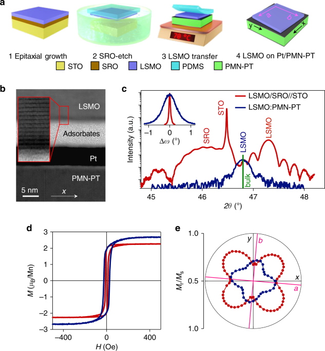
an opportunity in the development of laminated magnetoelectric memory devices. RESULTS SAMPLE FABRICATION AND CHARACTERIZATION An elastomer membrane of polydimethylsiloxane (PDMS) was used
to transfer a 45 nm-thick layer of LSMO from its STO (001) growth substrate to platinized PMN-PT (011)pc, after dissolving the intervening epitaxial layer of 30-nm-thick SRO with NaIO4 (aq)
(ref. 44) (Fig. 1a). The _a_ || [100]pc and _b_ || [010]pc axes of LSMO that lay parallel to the film edges were approximately aligned with the _x_ || [100]pc and _y_ || \(\left[ {01\bar 1}
\right]_{{\mathrm{pc}}}\) axes of PMN-PT that lay parallel to the edges of the slightly larger substrate (Supplementary Note 1). For simplicity, samples will be labelled LSMO:PMN-PT, without
reference to the Pt electrodes that are considered as if they were an integral part of the PMN-PT substrate, and without reference to an amorphous interfacial layer that we observed in
cross-sectional scanning transmission electron microscopy (STEM) (Fig. 1b). Chemical analysis revealed this interfacial layer of adsorbates to be primarily composed of SiO_x_ and C
(Supplementary Note 2), implying partial degradation of the PDMS membrane during the SRO etch. Two other polymers, which might have provided better mechanical support47, retained only small
LSMO flakes after etching. X-ray diffraction (XRD) measurements of our LSMO/SRO//STO (001) precursor confirmed that the LSMO layer experienced tensile in-plane epitaxial strain of ~1% (red
data, Fig. 1c) and a compressive out-of-plane strain of similar magnitude (Supplementary Note 3). The high quality of the LSMO film was confirmed by the presence of thickness fringes, and a
narrow 002pc rocking curve of full-width half-maximum 0.2° (red data, inset of Fig. 1c). Moreover, XRD reciprocal space maps around the STO 103 reflection confirmed a good match between the
in-plane lattice parameters of the LSMO, SRO and STO (Supplementary Note 3). XRD measurements of the LSMO film after it had been transferred to the platinized PMN-PT (011)pc substrate
revealed that the epitaxial strain had been completely released (blue data, Fig. 1c), and that the full-width-half-maximum of the 002pc rocking curve had increased to 1.7° (blue data, inset
of Fig. 1c). This enhancement of texture is attributed to the faceted PMN-PT (011)pc surface that necessarily results from ferroelectric domains of low symmetry (Supplementary Note 4), and
cracking in the LSMO film that arose at least in part while it was supported by the flexible PDMS membrane (Supplementary Note 5). The release of epitaxial strain increased the LSMO
saturation magnetization of 2.27 ± 0.03 _μ_B/Mn by 19% to 2.7 ± 0.1 _μ_B/Mn (Fig. 1d), which is roughly six times larger than the room-temperature saturation magnetization of highly strained
LSMO grown directly on PMN-PT (ref. 23). Similarly, the release of epitaxial strain led to an increase of Curie temperature (Supplementary Note 6), as expected48. The enhanced magnetism is
a consequence of enhanced double exchange following the release of epitaxial strain49, and should not be attributed to the oxidizing effect of the NaIO4 (aq) reagent on optimally doped films
that are well annealed. The release of epitaxial strain also modified the biaxial magnetic anisotropy of the LSMO film (Fig. 1e). After growth, the in-plane LSMO <110>pc directions
were magnetically easy due to magnetoelastic anisotropy arising from the biaxial in-plane strain imposed by the STO substrate45,50,51. After strain release and film transfer, the in-plane
LSMO <100>pc directions were magnetically easy due to uniaxial magnetocrystalline anisotropy in each twin variant of the now twinned film52 (Supplementary Note 7). Given that the
transfer process reduces the magnitude of the easy-axis anisotropy (Fig. 1e), the increase of easy-axis coercivity (Fig. 1d) is inferred to arise because of the observed cracks
(Supplementary Note 5) and any accompanying microstructural defects. ELECTRICALLY DRIVEN STRAIN IN PLATINIZED PMN-PT After thermally depolarizing PMN-PT in order to set zero strain, a
bipolar cycle of electric field _E_ produced orthogonal in-plane strains _ε__x_ and _ε__y_ that took opposite signs to each other at almost every field, and underwent sign reversal near the
coercive field (solid butterfly curves, Fig. 2a). Given that the two butterfly curves would be interchanged and different in magnitude if they arose purely from ferroelectric domain
switching in rhombohedral PMN-PT of nominally the same composition46, we infer that polarization reversal was instead associated with a phase transition11,12,13, as confirmed by measuring
XRD reciprocal space maps while applying an electric field (Supplementary Note 8). Large fields promoted the orthorhombic (O) phase by aligning the polarization along an out-of-plane
<011>pc direction, whereas switching through the coercive field promoted rhombohedral (R) twins whose polarizations lay along the subset of <111>pc directions with an
out-of-plane component. (A similar argument would hold if this latter phase were monoclinic53 rather than rhombohedral.) A minor electrical loop (blue dots in Fig. 2a) permitted two strain
states to be created in PMN-PT at electrical remanence12,46, with _ε__x_ = −0.16% in state A and _ε__x_ = + 0.02% in state B. The corresponding reciprocal space maps obtained at zero
electric field (Fig. 2b–e) show for our sample that the O phase dominated in state A (single 222pc reflection, split 031pc reflection), while the R phase dominated in state B (split 222pc
reflection, single 031pc reflection). The resulting structural changes in the LSMO film could also be detected by XRD (Supplementary Note 7), despite the twinning and the topography of the
underlying ferroelectric domains. STRAIN-MEDIATED ELECTRICAL CONTROL OF MACROSCOPIC MAGNETIZATION IN LSMO:PMN-PT The biaxial magnetic anisotropy that we observed after transfer (Fig. 1e) was
rendered uniaxial at both A and B during the course of 30 bipolar electrical cycles (Supplementary Note 9). Subsequent bipolar cycles modified the _x_ and _y_ components of magnetization by
~100% and ~40% (solid butterfly curves, Fig. 3), respectively, and similar results were observed for two similar samples (Supplementary Note 10). The peak magnetoelectric coefficient _α_ =
_µ_0d_M__x_/d_E_ = 6.4 × 10⁻⁸ s m−1 is similar to the value reported18 for an LSMO film that benefited from good epitaxial coupling with a PMN-PT (001) substrate. The interconversion of
remanent states A and B (blue dots in Fig. 3) rotated the single magnetic easy axis by 90° (Fig. 4), while the finite loop-squareness minimum in state B (Fig. 4d) may represent a vestige of
the original fourfold anisotropy, or uniaxial regions trapped from state A. STRAIN-MEDIATED ELECTRICAL CONTROL OF MICROSCOPIC MAGNETIZATION IN LSMO:PMN-PT The local magnetization of the
thermally demagnetized film was imaged using PEEM with contrast from XMCD. The resulting vector maps of the in-plane magnetization direction _ϕ_ revealed that the electrically remanent A and
B states were magnetically inhomogeneous within a 20 μm field of view (Fig. 5a, b); and that switching from A to B rotated the net magnetization in our limited field of view towards the
_x-_axis (Fig. 5c, d), consistent with our macroscopic measurements of magnetic anisotropy (Fig. 4c, d). The magnetization was reasonably homogeneous within few-micron-sized domains whose
boundaries coincided partly with cracks (Supplementary Note 11), and the electrically driven magnetic rotations in 1.3 μm-diameter regions (1–3 in Fig. 5a, b, e) ranged from large (64° in
region 1) to medium (−36° in region 2) to small (16° in region 3) (Fig. 5f). Although the clockwise and anticlockwise nature of these rotations could be explained in terms of the ambipolar
shear strains associated with rhombohedral ferroelectric domain switching54, the very different rotation magnitudes imply the presence of an additional factor. By assuming this additional
factor to be a spatially varying uniaxial magnetic anisotropy, due to spatially varying stress associated with the formation of the observed cracks (Supplementary Note 5), a magnetic free
energy model was able to approximately reproduce both the local and macroscopic magnetoelectric effects (Supplementary Note 12). DISCUSSION Our macroscopic magnetic measurements yield two
key results. First, growth using a well-matched substrate, followed by strain release via epitaxial lift-off28,29, resulted in an LSMO film magnetization that is greatly enhanced with
respect to the value for an LSMO film that contained strain and dislocations following direct growth on PMN-PT23. Second, our strain-mediated magnetoelectric coupling is just as effective as
strain-mediated coupling across an epitaxial interface17,18 in spite of the incoherent bonding between our magnetostrictive film and electroactive substrate. Our structurally contiguous
micron-sized regions were separated by cracks that could be avoided if one were to transfer micron-size patterned structures, or modify the procedure and transfer millimetre-sized crack-free
films36. However, the presence of cracks was instructive because the resulting micromechanical boundary conditions likely served to influence the magnetic rotations of our micron-size
magnetic domains. Close control of these boundary conditions via lithographic patterning would permit a transferred ferromagnetic film to function as the electrically controlled free layer
of a magnetic tunnel junction for data-storage applications14,15,16, and the free choice of in-plane misorientation angle would permit the realization of schemes for electrically driven
magnetization reversal55,56,57. As we have shown, the magnetization would not suffer from the epitaxial suppression that compromises oxide device performance58. More generally, the physical
and chemical properties of any epitaxially grown film could be electrically controlled via strain after transfer to an electroactive substrate, with no constraints on relative
crystallographic orientation, and no epitaxial strain to suppress film functional properties. Separately, it would be interesting to investigate strain-mediated coupling while varying the
thickness and composition of the interfacial glue that formed here serendipitously. It would also be interesting to better support the LSMO film during transfer in order to avoid the
observed cracks. Ultimately, electroactive substrates themselves could be replaced by electroactive films that have been released in order to avoid substrate clamping59. Our work therefore
opens the way for multifunctional heterostructures to be assembled from epitaxial oxides via mechanical separation and stacking, just as two-dimensional and other materials may be combined
using similar methods of van der Waals integration30. These multifunctional heterostructures could then be transferred to silicon host structures in the wider-ranging quest for CMOS
compatibility. METHODS SAMPLES We fabricated three similar LSMO:PMN-PT samples (A, B and C). The LSMO film (edges along _a_ || [100]pc and _b_ || [010]pc) was misaligned with the PMN-PT
substrate (edges along _x_ || [100]pc and _y_ || \(\left[ {01\bar 1} \right]_{{\mathrm{pc}}}\)) by 5° (samples A, B) and 20° (sample C). All experimental data were obtained using sample A or
its precursor components, with the following exceptions: measurements of strain and electrical polarization were obtained using PMN-PT from the same master substrate that we used for sample
A; atomic force microscopy (AFM) data were obtained using sample B; STEM data were obtained using sample C; the Curie temperature measurements in Supplementary Fig. 6 were obtained using
similar samples; and the macroscopic magnetoelectric data in Supplementary Fig. 10 were obtained using samples A–C. EPITAXIAL GROWTH OF LSMO/SRO BILAYERS Epitaxial LSMO (45 nm)/SRO (30 nm)
bilayers were grown by pulsed laser deposition (KrF excimer laser, 248 nm, 1 Hz) on STO (001) substrates (5 mm × 5 mm × 1 mm) that had been annealed in flowing oxygen for 90 min at 950 °C.
The SRO was grown in 10 Pa O2 at 600 °C (1200 pulses, 1.5 J cm−2). The LSMO was grown in 15 Pa O2 at 760 °C (1800 pulses, 2 J cm−2). After growth, the LSMO/SRO//STO stacks underwent in situ
annealing in 50 kPa O2 for 1 h at 700 °C. Using X-ray reflectivity measurements, the growth rates for single layers of SRO and LSMO were both found to be ~0.025 nm per pulse. PLATINIZED
PMN-PT SUBSTRATES Each 0.68Pb(Mg1/3Nb2/3)O3–0.32PbTiO3 (011)pc substrate (PMN-PT; Atom Optics) was cut to ~5 mm × ~5 mm × 0.3 mm from a different 10 mm × 10 mm × 0.3 mm master. Sputter
deposition of Pt resulted in a 6-nm-thick top electrode that served as ground, and a much thicker bottom electrode. TRANSFER OF LSMO PDMS stamps were cut to 5 mm × 5 mm × 1.5 mm from a
commercial specimen (Gelfilm from Gelpak), and each was brought into conformal contact with a given LSMO/SRO//STO stack by heating in air at 70 °C for 10 min (conformal contact was verified
by the change in optical reflectance on elimination of the air gap). After floating the resulting PDMS/LSMO/SRO//STO stacks in NaIO4 (aq) (0.4 M) for several hours, the SRO layers dissolved
to release bilayers of PDMS/LSMO, which were washed with deionized water, and dried with N2 gas. Using tweezers, each PDMS/LSMO bilayer was subsequently transferred to a platinized PMN-PT
substrate, which had been previously cleaned using acetone and isopropanol, and recently cleaned by annealing in air at 120 °C for 10 min. After transfer, the entire stack was annealed in
air (at 100 °C for 10 min) to promote adhesion at the newly formed interface. After cooling to 70 °C and peeling off the PDMS stamp with tweezers, interfacial adhesion was further improved
by annealing in air at 150 °C for 10 min. X-RAY DIFFRACTION We acquired 2_θ_–_ω_ scans and rocking curves for LSMO with a Panalytical Empyrean diffractometer (Cu-Kα1, 1.540598 Å), using a
hybrid two-bounce primary monochromator on the incident beam, and a two-bounce analyser crystal before the proportional point detector. Reciprocal space maps of PMN-PT were acquired with the
same incident beam optics and a PIXcel3D position-sensitive detector, using the frame-based 1D mode with a step time of 10 s. We used Sample A and its epitaxial precursor to obtain 2_θ_–_ω_
scans and rocking curves before applying an electric field (Fig. 1c). For the transferred LSMO film in Sample A, offset angle _ω_ was obtained by averaging the rocking-curve-peak-values for
azimuthal angles of _φ_ = 0° and _φ_ = 180°. Our electric-field-dependent XRD data were also obtained using sample A, after acquiring a subset of the magnetoelectric data and then repeating
the last anneal of the fabrication process (10 min in air at 150 °C) in order to depolarize the substrate. We first obtained reciprocal space maps of PMN-PT at successively larger positive
fields after negative poling (Supplementary Fig. 5d, e), before acquiring reciprocal space maps for remanent states A and B (Fig. 2b–d). We then obtained 2_θ_–_ω_ scans of LSMO for remanent
states A and B (Supplementary Fig. 6). ATOMIC FORCE MICROSCOPY Atomic force microscopy (AFM) images were obtained in tapping mode using a Veeco Digital Instruments Dimension D3100
microscope. ELECTRON MICROSCOPY Cross-sectional transmission electron microscopy (TEM) specimens were prepared via an in situ lift-out procedure in a dual-beam instrument (FEI Nova 600i)
that incorporated a focused ion beam microscope and scanning electron microscope in the same chamber. Both 5 and 2 kV ions were used to polish the TEM lamella to a thickness of 50 nm, and
remove side damage. High-resolution scanning transmission electron microscopy (STEM) was performed using a probe-side aberration-corrected FEI Titan G2, operated at 80–200 kV with a
high-brightness field-emission gun (X-FEG). Bright-field STEM imaging was performed using a probe convergence angle of 21 mrad and a probe current of ∼90 pA. In bright-field images,
identification of each atomic layer was achieved by elemental analysis using energy dispersive X-ray (EDX) and electron energy loss spectroscopy (EELS). EDX images were obtained using a
Super-X four silicon drift EDX detector system with a total-collection solid angle of 0.7 sr. EELS images were obtained using a Gatan Imaging Filter (GIF) Quantum ER system, with an entrance
aperture of 5 mm. The lamella was oriented by using the Kikuchi bands to direct the electron beam down the \(\left[ {01\bar 1} \right]_{{\mathrm{pc}}}\) zone axis of PMN-PT. STRAIN
MEASUREMENTS Platinized PMN-PT (derived from the master substrate used for sample A) was cleaned like sample A, using acetone and isopropanol, and then annealed in air at 150 °C for 30 min
in order to mimic the final depolarizing heat treatment experienced by sample A. A biaxial strain gauge (KFG-1-120-D16-16 L1M3S, Kyowa) was affixed using glue (CC-33A strain gauge cement,
Kyowa) to the top electrode, with measurement axes along _x_ and _y_. The initial values of resistance were used to identify zero strain along the two measurement directions. Strain-field
data were obtained while applying bipolar triangular voltages at 0.01 Hz in the range ±10 kV cm−1. MACROSCOPIC MAGNETIZATION MEASUREMENTS These were performed using a Princeton Measurements
Corporation vibrating sample magnetometer, with electrical access to the sample as shown in ref. 17. All data are presented after subtracting the diamagnetic contribution of substrate, and
using optical microscopy to estimate film areas. MAGNETIC VECTOR MAPS After completing all macroscopic magnetoelectric measurements, we obtained raw images of sample A after thermal
demagnetization. The electrically remanent states A and B were interconverted in situ using a 300 V power supply that was connected via feedthroughs in the sample holder. Data were obtained
on beamline I06 at Diamond Light Source, where we used an Elmitec SPELEEM-III microscope to map secondary-electron emission arising from circularly polarized X-rays that were incident on the
sample surface at a grazing angle of 16°. The probe depth was ∼7 nm, and the lateral resolution in our 20 μm-diameter field of view was typically ∼50 nm (corresponding to pixels that
represent ~20 nm). Raw images were acquired during 1 s exposure times with right (R) and left (L) circularly polarized light, both on the Mn _L_3 resonance at 645.5 eV, and off this
resonance at 642 eV. The pixels in a raw XMCD-PEEM image describe the XMCD asymmetry (_I_R − _I_L)/(_I_R + _I_L), which represents the projection of the local surface magnetization on the
incident-beam direction. Here, \(I^{{\mathrm{R/L}}} = ( {I_{{\mathrm{on}}}^{{\mathrm{R/L}}} - I_{{\mathrm{off}}}^{{\mathrm{R/L}}}} )/I_{{\mathrm{off}}}^{{\mathrm{R/L}}}\) denotes the
relative intensity for secondary-electron emission due to X-ray absorption on \(( {I_{{\mathrm{on}}}^{{\mathrm{R/L}}}})\) and off \(( {I_{{\mathrm{off}}}^{{\mathrm{R/L}}}} )\) the Mn _L_3
resonance (the comparison between intensities obtained on and off resonance avoids the influence of any inhomogeneous illumination). We averaged 40 raw XMCD-PEEM images to obtain a single
XMCD-PEEM image for each of two orthogonal sample orientations. These two images were combined in order to yield vector maps of in-plane magnetization, which are not necessarily perfectly
circular after correcting for drift and distortion via an affine transformation that was based on topographical images of X-ray absorption for each sample orientation. Each of these
topographical images was obtained by averaging all raw images that had been obtained on resonance with left- and right-polarized light. XAS IMAGES X-ray absorption spectroscopy images are
presented alongside XMCD-PEEM images (Supplementary Note 11) by plotting (_I_R + _I_L) and (_I_R − _I_L)/(_I_R + _I_L), respectively. DATA AVAILABILITY The source data underlying Figs. 1c–e,
2a, 3, 4a–d and 5c–f are provided in a Source Data file. All other relevant data are available from all corresponding authors on request. Source data are provided with this paper.
REFERENCES * Tokura, Y. Orbital physics in transition-metal oxides. _Science_ 288, 462–468 (2000). Article ADS CAS PubMed Google Scholar * Hwang, H. Y. et al. Emergent phenomena at
oxide interfaces. _Nat. Mater._ 11, 103–113 (2012). Article ADS CAS PubMed Google Scholar * Weber, M. C. et al. Multiple strain-induced phase transitions in LaNiO3 thin films. _Phys.
Rev. B_ 94, 014118 (2016). Article ADS CAS Google Scholar * Mayeshiba, T. & Morgan, D. Strain effects on oxygen vacancy formation energy in perovskites. _Solid State Ionics_ 311,
105–117 (2017). Article CAS Google Scholar * Aetukuri, N. B. et al. Control of the metal-insulator transition in vanadium dioxide by modifying orbital occupancy. _Nat. Phys._ 9, 661–666
(2013). Article CAS Google Scholar * Pan, X. Q. et al. Enhancement of ferroelectricity in strained BaTiO3 thin films. _Science_ 306, 1005–1009 (2004). Article ADS PubMed CAS Google
Scholar * Konishi, Y. et al. Orbital-state-mediated phase-control of manganites. _J. Phys. Soc. Japan_ 68, 3790–3793 (1999). Article ADS CAS Google Scholar * Hwang, J. et al. Tuning
perovskite oxides by strain: electronic structure, properties, and functions in (electro)catalysis and ferroelectricity. _Mater. Today_ 31, 100–118 (2019). Article CAS Google Scholar *
Petrie, J. R. et al. Enhanced bifunctional oxygen catalysis in strained LaNiO3 perovskites. _J. Am. Chem. Soc._ 138, 2488–2491 (2016). Article CAS PubMed Google Scholar * Park, S.-E.
& Shrout, T. R. Ultrahigh strain and piezoelectric behavior in relaxor based ferroelectric single crystals. _J. Appl. Phys._ 82, 1804–1811 (1997). Article ADS CAS Google Scholar *
Wang, Z., Wang, Y., Luo, H., Li, J. & Viehland, D. Crafting the strain state in epitaxial thin films: a case study of CoFe2O4 films on Pb(Mg,Nb)O3−PbTiO3. _Phys. Rev. B_ 90, 134103
(2014). Article ADS CAS Google Scholar * Wang, Z., Wang, Y., Ge, W., Li, J. & Viehland, D. Volatile and nonvolatile magnetic easy-axis rotation in epitaxial ferromagnetic thin films
on ferroelectric single crystal substrates. _Appl. Phys. Lett._ 103, 132909 (2013). Article ADS CAS Google Scholar * Gilbert, I. et al. Magnetic microscopy and simulation of
strain-mediated control of magnetization in PMN-PT/Ni nanostructures. _Appl. Phys. Lett._ 109, 162404 (2016). Article ADS PubMed PubMed Central CAS Google Scholar * Matsukura, F.,
Tokura, Y. & Ohno, H. Control of magnetism by electric fields. _Nat. Nanotechnol._ 10, 209–220 (2015). Article ADS CAS PubMed Google Scholar * Fusil, S., Garcia, V., Barthélémy, A.
& Bibes, M. Magnetoelectric devices for spintronics. _Annu. Rev. Mater. Res._ 44, 91–116 (2014). Article ADS CAS Google Scholar * Hu, J. M., Li, Z., Chen, L. Q. & Nan, C. W.
High-density magnetoresistive random access memory operating at ultralow voltage at room temperature. _Nat. Commun._ 2, 553–558 (2011). Article ADS PubMed PubMed Central CAS Google
Scholar * Eerenstein, W., Wiora, M., Prieto, J. L., Scott, J. F. & Mathur, N. D. Giant sharp and persistent converse magnetoelectric effects in multiferroic epitaxial heterostructures.
_Nat. Mater._ 6, 348–351 (2007). Article ADS CAS PubMed Google Scholar * Thiele, C., Dörr, K., Bilani, O., Rödel, J. & Schultz, L. Influence of strain on the magnetization and
magnetoelectric effect in La0.7A0.3MnO3/PMN-PT(001) (_A_=Sr,Ca). _Phys. Rev. B_ 75, 054408 (2007). Article ADS CAS Google Scholar * Moya, X. et al. Giant and reversible extrinsic
magnetocaloric effects in La0.7Ca0.3MnO3 films due to strain. _Nat. Mater._ 12, 52–58 (2013). Article ADS CAS PubMed Google Scholar * Dale, D., Fleet, A., Brock, J. D. & Suzuki, Y.
Dynamically tuning properties of epitaxial colossal magnetoresistance thin films. _Appl. Phys. Lett._ 82, 3725 (2003). Article ADS CAS Google Scholar * Heo, S. et al. Modulation of
metal-insulator transitions by field-controlled strain in NdNiO3/SrTiO3/PMN-PT (001) heterostructures. _Sci. Rep._ 6, 22228 (2016). Article ADS CAS PubMed PubMed Central Google Scholar
* Zhang, W. et al. Piezostrain-enhanced photovoltaic effects in BiFeO3/La0.7Sr0.3MnO3/PMN-PT heterostructures. _Nano Energy_ 18, 315–324 (2015). Article CAS Google Scholar * Xu, H. et
al. Strain-mediated converse magnetoelectric coupling in La0.7Sr0.3MnO3/Pb(Mg1/3Nb2/3)O3–PbTiO3 multiferroic heterostructures. _Cryst. Growth Des._ 18, 5934–5939 (2018). Article CAS Google
Scholar * Kim, J. Y., Yao, L. & Van Dijken, S. Coherent piezoelectric strain transfer to thick epitaxial ferromagnetic films with large lattice mismatch. _J. Phys. Condens. Matter_ 25,
082205 (2013). Article ADS PubMed CAS Google Scholar * Park, J. H. et al. In-plane strain control of the magnetic remanence and cation-charge redistribution in CoFe2O4 thin film grown
on a piezoelectric substrate. _Phys. Rev. B_ 81, 134401 (2010). Article ADS CAS Google Scholar * Zhou, W. P. et al. Electric field manipulation of magnetic and transport properties in
SrRuO3/Pb(Mg1/3Nb2/3)O3-PbTiO3 heterostructure. _Sci. Rep._ 4, 6991 (2014). Article CAS PubMed PubMed Central Google Scholar * Bilani-Zeneli, O. et al. SrTiO3 on piezoelectric
PMN-PT(001) for application of variable strain. _J. Appl. Phys._ 104, 054108 (2008). Article ADS CAS Google Scholar * Demeester, P., Pollentier, I., Dobbelaere, P. D. E., Brys, C. &
Daele, P. V. A. N. Epitaxial lift-off and its applications. _Semicond. Sci. Technol._ 8, 1124–1135 (1993). Article ADS CAS Google Scholar * Konagai, M., Sugimoto, M. & Takahashi, K.
High efficiency GaAs thin film solar cells by peeled film technology. _J. Cryst. Growth_ 45, 277–280 (1978). Article ADS CAS Google Scholar * Liu, Y., Huang, Y. & Duan, X. Van der
Waals integration before and beyond two-dimensional materials. _Nature_ 567, 323–333 (2019). Article ADS CAS PubMed Google Scholar * Cheng, C. W. et al. Epitaxial lift-off process for
gallium arsenide substrate reuse and flexible electronics. _Nat. Commun._ 4, 1577 (2013). Article ADS PubMed CAS Google Scholar * Kim, Y. et al. Remote epitaxy through graphene enables
two-dimensional material-based layer transfer. _Nature_ 544, 340–343 (2017). Article ADS CAS PubMed Google Scholar * Gan, Q. et al. Direct measurement of strain effects on magnetic and
electrical properties of epitaxial SrRuO3 thin films. _Appl. Phys. Lett._ 72, 978–980 (1998). Article ADS CAS Google Scholar * Paskiewicz, D. M., Sichel-Tissot, R., Karapetrova, E.,
Stan, L. & Fong, D. D. Single-crystalline SrRuO3 nanomembranes: a platform for flexible oxide electronics. _Nano Lett._ 16, 534–542 (2016). Article ADS CAS PubMed Google Scholar *
Bakaul, S. R. et al. Single crystal functional oxides on silicon. _Nat. Commun._ 7, 10547 (2016). Article ADS CAS PubMed PubMed Central Google Scholar * Lu, D. et al. Synthesis of
freestanding single-crystal perovskite films and heterostructures by etching of sacrificial water-soluble layers. _Nat. Mater._ 15, 1255–1260 (2016). Article ADS CAS PubMed Google
Scholar * Chen, Z. et al. Freestanding crystalline YBa2Cu3O7 heterostructure membranes. _Phys. Rev. Mater._ 3, 060801 (2019). Article CAS Google Scholar * Bakaul, S. R. et al. High speed
epitaxial perovskite memory on flexible substrates. _Adv. Mater._ 29, 1605699 (2017). Article CAS Google Scholar * Shen, L. et al. Epitaxial lift-off of centimeter-scaled spinel ferrite
oxide thin films for flexible electronics. _Adv. Mater._ 29, 1702411 (2017). Article CAS Google Scholar * Luo, Z.-D., Peters, J. J. P., Sanchez, A. M. & Alexe, M. Flexible memristors
based on single-crystalline ferroelectric tunnel junctions. _ACS Appl. Mater. Interfaces_ 11, 23313–23319 (2019). Article CAS PubMed Google Scholar * Wang, H. et al. Integration of both
invariable and tunable microwave magnetisms in a single flexible La0.67Sr0.33MnO3 thin film. _ACS Appl. Mater. Interfaces_ 11, 22677–22683 (2019). Article CAS PubMed Google Scholar *
Hong, S. S. et al. Extreme tensile strain states in La0.7Ca0.3MnO3 membranes. _Science_ 368, 71–76 (2020). Article ADS CAS PubMed Google Scholar * Hui, Y. Y. et al. Exceptional
tunability of band energy in a compressively strained trilayer MoS2 sheet. _ACS Nano_ 7, 7126–7131 (2013). Article CAS PubMed Google Scholar * Weber, D., Vofély, R., Chen, Y., Mourzina,
Y. & Poppe, U. Variable resistor made by repeated steps of epitaxial deposition and lithographic structuring of oxide layers by using wet chemical etchants. _Thin Solid Films_ 533, 43–47
(2013). Article ADS CAS Google Scholar * Steenbeck, K. & Hiergeist, R. Magnetic anisotropy of ferromagnetic La0.7(Sr,Ca)0.3MnO3 epitaxial film. _Appl. Phys. Lett._ 75, 1778–1780
(1999). Article ADS CAS Google Scholar * Wu, T. et al. Domain engineered switchable strain states in ferroelectric (011) [Pb(Mg1/3Nb2/3)O3](1-x)-[PbTiO3]x (PMN-PT, x≈0.32) single
crystals. _J. Appl. Phys._ 109, 124101 (2011). Article ADS CAS Google Scholar * Wang, J. I. J. et al. Electronic transport of encapsulated graphene and WSe2 devices fabricated by pick-up
of prepatterned hBN. _Nano Lett._ 15, 1898–1903 (2015). Article ADS CAS PubMed Google Scholar * Millis, A. J., Darling, T. & Migliori, A. Quantifying strain dependence in
‘colossal’ magnetoresistance manganites. _J. Appl. Phys._ 83, 1588–1591 (1998). Article ADS CAS Google Scholar * Fang, Z., Solovyev, I. & Terakura, K. Phase diagram of tetragonal
manganites. _Phys. Rev. Lett._ 84, 3169–3172 (2000). Article ADS CAS PubMed Google Scholar * Lecoeur, P. et al. Magnetic domain structures of La0.67Sr0.33MnO3 thin films with different
morphologies. _J. Appl. Phys._ 82, 3934–3939 (1997). Article ADS CAS Google Scholar * Berndt, L. M., Balbarin, V. & Suzuki, Y. Magnetic anisotropy and strain states of (001) and
(110) colossal magnetoresistance thin films. _Appl. Phys. Lett._ 77, 2903–2905 (2000). Article ADS CAS Google Scholar * Suzuki, Y. et al. Magnetic anisotropy of doped manganite thin
films and crystals. _J. Appl. Phys._ 83, 7064–7066 (1998). Article ADS CAS Google Scholar * Cao, H. et al. Intermediate ferroelectric orthorhombic and monoclinic _M_ _B_ phases in [110]
electric-field-cooled Pb(Mg1/3Nb2/3)O3-30%PbTiO3 crystals. _Phys. Rev. B_ 72, 064104 (2005). Article ADS CAS Google Scholar * Ghidini, M. et al. Shear-strain-mediated magnetoelectric
effects revealed by imaging. _Nat. Mater._ 18, 840–845 (2019). Article ADS CAS PubMed Google Scholar * Iwasaki, Y. Stress-driven magnetization reversal in magnetostrictive films with
in-plane magnetocrystalline anisotropy. _J. Magn. Magn. Mater._ 240, 395–397 (2002). Article ADS CAS Google Scholar * Peng, R.-C. et al. Fast 180° magnetization switching in a
strain-mediated multiferroic heterostructure driven by a voltage. _Sci. Rep_. 6, 27561 (2016). Article ADS CAS PubMed PubMed Central Google Scholar * Peng, R. C., Wang, J. J., Hu, J.
M., Chen, L. Q. & Nan, C. W. Electric-field-driven magnetization reversal in square-shaped nanomagnet-based multiferroic heterostructure. _Appl. Phys. Lett._ 106, 142901 (2015). Article
ADS CAS Google Scholar * Dekker, M. C. et al. Magnetoelastic response of La0.7Sr0.3MnO3/SrTiO3 superlattices to reversible strain. _Phys. Rev. B_ 84, 054463 (2011). Article ADS CAS
Google Scholar * Nagarajan, V. et al. Dynamics of ferroelastic domains in ferroelectric thin films. _Nat. Mater._ 2, 43–47 (2003). Article ADS CAS PubMed Google Scholar * Radaelli, P.
G. et al. Structural effects on the magnetic and transport properties of perovskite \({A_{1-x}}{A^{\prime}_{x}}{\mathrm{MnO}_{3}}(x=0.25, 0.30)\). _Phys. Rev. B_ 56, 8265–8276 (1997).
Article ADS CAS Google Scholar Download references ACKNOWLEDGEMENTS D.P. acknowledges Agència de Gestió d’Ajuts Universitaris i de Recerca (AGAUR) from the Catalan government for Beatriu
de Pinós postdoctoral fellowship (2014 BP-A 00079). E.K. acknowledges support by the Ministry of Science and Higher Education of Russian Federation, goszadanie no. 2019-1246. X.M.
acknowledges funding from the Royal Society. We thank Diamond Light Source for time on beamline I06 (proposal SI14745-1). S.J.H. and A.P.R. acknowledge funding from EPSRC (Grant
EP/P009050/1, EP/M010619/1 and the NoWNano DTC) and the European Research Council (ERC) (ERC-2016-STG-EvoluTEM-715502 and ERC Synergy HETERO2D). P.R. acknowledges funding by the ‘la
Caixa' Foundation (ID 100010434). We thank Jiamian Hu, Manish Chhowalla, Emilio Artacho, Paul Attfield, Sohini Kar-Narayan and Judith Driscoll for discussions. AUTHOR INFORMATION
AUTHORS AND AFFILIATIONS * Department of Materials Science, University of Cambridge, Cambridge, CB3 0FS, UK D. Pesquera, M. Ghidini, S. Zhang, P. Riego, J. Kim, X. Moya, M. E. Vickers, N. A.
Stelmashenko & N. D. Mathur * ITMO University, Saint Petersburg, 197101, Russia E. Khestanova * Department of Mathematics, Physics and Computer Science, University of Parma, 43124,
Parma, Italy M. Ghidini * Diamond Light Source, Chilton, Didcot, Oxfordshire, OX11 0DE, UK M. Ghidini, F. Maccherozzi & S. S. Dhesi * College of Science, National University of Defense
Technology, Changsha, 410073, China S. Zhang * School of Materials, University of Manchester, Manchester, M13 9PL, UK A. P. Rooney & S. J. Haigh * CIC nanoGUNE, E-20018, Donostia-San
Sebastian, Spain P. Riego * Department of Condensed Matter Physics, University of the Basque Country, UPV/EHU, E-48080, Bilbao, Spain P. Riego * Zernike Institute for Advanced Materials,
University of Groningen, 9747 AG, Groningen, The Netherlands S. Farokhipoor Authors * D. Pesquera View author publications You can also search for this author inPubMed Google Scholar * E.
Khestanova View author publications You can also search for this author inPubMed Google Scholar * M. Ghidini View author publications You can also search for this author inPubMed Google
Scholar * S. Zhang View author publications You can also search for this author inPubMed Google Scholar * A. P. Rooney View author publications You can also search for this author inPubMed
Google Scholar * F. Maccherozzi View author publications You can also search for this author inPubMed Google Scholar * P. Riego View author publications You can also search for this author
inPubMed Google Scholar * S. Farokhipoor View author publications You can also search for this author inPubMed Google Scholar * J. Kim View author publications You can also search for this
author inPubMed Google Scholar * X. Moya View author publications You can also search for this author inPubMed Google Scholar * M. E. Vickers View author publications You can also search for
this author inPubMed Google Scholar * N. A. Stelmashenko View author publications You can also search for this author inPubMed Google Scholar * S. J. Haigh View author publications You can
also search for this author inPubMed Google Scholar * S. S. Dhesi View author publications You can also search for this author inPubMed Google Scholar * N. D. Mathur View author publications
You can also search for this author inPubMed Google Scholar CONTRIBUTIONS D.P. and N.D.M. designed and led the project. D.P. and E.K. fabricated the samples with assistance from N.A.S. D.P.
performed the X-ray diffraction measurements with assistance from M.E.V. A.P.R. and S.J.H. were responsible for the electron microscopy. D.P. acquired the atomic force microscopy data. D.P.
performed the electric-field-dependent measurements of magnetization and strain with assistance from M.G. J.K. acquired the temperature-dependent magnetization data. D.P., M.G., F.M., P.R.,
S.F. and X.M. collected and analysed the XMCD-PEEM data under the supervision of S.S.D. D.P. constructed and analysed the magnetic vector maps. S.Z. performed the magnetic free energy
simulations. N.D.M. wrote the manuscript with D.P., using substantive feedback from M.G., and additional feedback from E.K., S.Z., P.R., X.M., M.E.V., S.J.H. and S.S.D. CORRESPONDING AUTHORS
Correspondence to D. Pesquera or N. D. Mathur. ETHICS DECLARATIONS COMPETING INTERESTS The authors declare no competing interests. ADDITIONAL INFORMATION PEER REVIEW INFORMATION _Nature
Communications_ thanks Yasuyuki Hikita, Haibo Li and the other, anonymous, reviewer(s) for their contribution to the peer review of this work. Peer reviewer reports are available.
PUBLISHER’S NOTE Springer Nature remains neutral with regard to jurisdictional claims in published maps and institutional affiliations. SUPPLEMENTARY INFORMATION SUPPLEMENTARY INFORMATION
PEER REVIEW FILE SOURCE DATA SOURCE DATA RIGHTS AND PERMISSIONS OPEN ACCESS This article is licensed under a Creative Commons Attribution 4.0 International License, which permits use,
sharing, adaptation, distribution and reproduction in any medium or format, as long as you give appropriate credit to the original author(s) and the source, provide a link to the Creative
Commons license, and indicate if changes were made. The images or other third party material in this article are included in the article’s Creative Commons license, unless indicated
otherwise in a credit line to the material. If material is not included in the article’s Creative Commons license and your intended use is not permitted by statutory regulation or exceeds
the permitted use, you will need to obtain permission directly from the copyright holder. To view a copy of this license, visit http://creativecommons.org/licenses/by/4.0/. Reprints and
permissions ABOUT THIS ARTICLE CITE THIS ARTICLE Pesquera, D., Khestanova, E., Ghidini, M. _et al._ Large magnetoelectric coupling in multiferroic oxide heterostructures assembled via
epitaxial lift-off. _Nat Commun_ 11, 3190 (2020). https://doi.org/10.1038/s41467-020-16942-x Download citation * Received: 23 October 2019 * Accepted: 02 June 2020 * Published: 24 June 2020
* DOI: https://doi.org/10.1038/s41467-020-16942-x SHARE THIS ARTICLE Anyone you share the following link with will be able to read this content: Get shareable link Sorry, a shareable link is
not currently available for this article. Copy to clipboard Provided by the Springer Nature SharedIt content-sharing initiative