- Select a language for the TTS:
- UK English Female
- UK English Male
- US English Female
- US English Male
- Australian Female
- Australian Male
- Language selected: (auto detect) - EN
Play all audios:
ABSTRACT To fully exploit van der Waals materials and their vertically stacked heterostructures, new mass-scalable production routes which are low cost but preserve the high electronic and
optical quality of the single crystals are required. Here, we demonstrate an approach to realise a variety of functional heterostructures based on van der Waals nanocrystal films produced
through the mechanical abrasion of bulk powders. We find significant performance enhancements in abraded heterostructures compared to those fabricated through inkjet printing of nanocrystal
dispersions. To highlight the simplicity, applicability and scalability of the device fabrication, we demonstrate a multitude of different functional heterostructures such as resistors,
capacitors and photovoltaics. We also demonstrate the creation of energy harvesting devices, such as large area catalytically active coatings for the hydrogen evolution reaction and enhanced
triboelectric nanogenerator performance in multilayer films. The ease of device production makes this a promising technological route for up-scalable films and heterostructures. SIMILAR
CONTENT BEING VIEWED BY OTHERS VAN DER WAALS HETEROSTRUCTURES Article 28 July 2022 A ROUTE TOWARDS THE FABRICATION OF LARGE-SCALE AND HIGH-QUALITY PEROVSKITE FILMS FOR OPTOELECTRONIC DEVICES
Article Open access 06 May 2022 VERSATILE CONSTRUCTION OF VAN DER WAALS HETEROSTRUCTURES USING A DUAL-FUNCTION POLYMERIC FILM Article Open access 15 June 2020 INTRODUCTION High-quality van
der Waals (vdW) heterostructures are produced by stacking together different two-dimensional (2D) materials1,2. The properties are highly customisable depending on the component materials
and the layer sequence, providing use in a wide variety of applications. Compared with conventional compound semiconductor heterostructure devices, they have the potential to offer many
advantages. For instance, they are lightweight, semi-transparent and are compatible with flexible substrates, whilst displaying competitive performance. The highest quality vdW
heterostructures out-perform conventional materials, but they are still mainly constructed by mechanical exfoliation of bulk single crystals and built up layer-by-layer by standard
mechanical transfer procedures1,2,3. However, this precise yet enormously time-consuming method is not scalable and alternative device manufacturing routes are urgently required to achieve
widespread uptake of these materials. Chemical vapour deposition (CVD)4 is a promising synthesis approach for vdW heterostructures, where monolayer films are sequentially grown
layer-by-layer at high temperatures, with some of the resulting material heterostructures beginning to approach the performance levels of exfoliated crystals. However, the initial investment
required and energy cost of CVD growth is high for a given quantity of monolayer material produced. Furthermore, the growth of multilayer systems becomes increasingly complex with the
approach confined to a small number of 2D material combinations. Finally, CVD growth requires the use of catalyst substrates and subsequent transfer of the heterostructure films; this often
introduces undesirable contamination, tears and cracks which prevent the formation of high-quality vertical heterostructure devices4. An alternative low-cost route for mass-scalable
production of nanocrystal heterostructures is through printing of liquid phase exfoliated (LPE) dispersions5,6,7. In this scheme, the vdW material dispersions are produced through either
ultra-sonication or shear force exfoliation of bulk vdW microcrystals in suitable solvents8. This leads to stable dispersions which can then be subsequently printed on a variety of
substrates. By mixing the dispersions with specialist binders heterostructures can also be built up layer-by-layer5. However, strong disorder in the crystals caused by oxidation, small
crystallite size and poor interface quality leads to severe performance degradation compared with devices based on mechanically exfoliated or CVD grown 2D films. In addition, this production
method is unlikely to be compatible with the many highly air sensitive vdW materials that are attracting considerable interest recently due to their exotic properties9,10, limiting the
scope of this technology. Moreover, residual solvent in the printed films has been shown to degrade the electrical properties of the devices by further reducing the quality of the interface
between neighbouring nanocrystals11. This work sets out a route to build up semi-transparent and flexible vdW nanocrystal heterostructures through the simplest possible technique that is
through a mechanical abrasion process. Here, we show that high-quality electronic and optoelectronic heterostructures can be readily fabricated within a matter of minutes on the scale of 10s
of cm and could easily be scaled up further. The production of rubbed/abraded films have yielded flexible conductive graphite coatings and triboelectric properties in abraded intercalated
graphite on steel12,13. However, to date, no demonstration of multilayer electronic/optoelectronic devices have been shown. Most surprisingly, using high-resolution scanning transmission
electron microscopy (STEM), we observe sharp heterointerfaces formed as a result of the direct abrasion process, which has the potential to facilitate a wide variety of different devices
through this approach. Specifically, in this work we focus on combining several vdW materials including graphite, MoS2, WS2, MoSe2 and hexagonal boron nitride (hBN). In order to highlight
the applicability of the abrasive method we show several examples of electronic and optoelectronic heterostructures including thin graphite field effect transistors, vertical transition
metal dichalcogenide (TMDC) photodetectors, photovoltaics, hBN capacitors, hydrogen evolution reaction (HER) catalysts and multilayer films for triboelectric nanogenerator (TENG), many of
which show significant improvements in device performance compared with those produced by inkjet printing of LPE materials. RESULTS DEVICE CHARACTERISATION AND FABRICATION The general
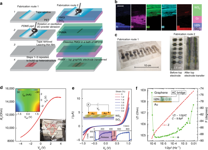
approach used to produce thin films and devices on SiO2 as well as polymer substrates is shown in Fig. 1a. Essentially, we make use of a viscoelastic polymer, namely polydimethylsiloxane
(PDMS), which is cut into 1 cm × 1 cm sections and then pressed into a bulk vdW material powder (graphite, TMDCs, etc). This ensures full adhesion of the micron-sized powder particles to the
PDMS surface and allows it to be used as a writing pad. All of the powders investigated adhere equally well to the surface of the PDMS. The PDMS pad is then oscillated back and forth
against the substrate with vdW materials embedded between it. We expect that the key parameters which govern the abrasion process on different substrates include the substrate roughness, vdW
material hardness14 and the relative position on the triboelectric series15 between the vdW material and the substrate (electrostatic charging). Subsequent deposition of material is then
due to a friction-facilitated basal cleavage of micro-crystallites within the bulk material powder as it is rubbed against the layers already adhered to the substrate, overall resulting in
the deposition of a thin abraded nanocrystalline film. The thickness of the deposited material is controlled by the rubbing time and the force applied to the writing pad. To better quantify
the abrasion process we also modified a computer numerical control (CNC) micro engraver system to study the effect of force, feed rate and the sheet resistance vs number of write passes as
discussed in “Device fabrication” under “Methods” section and in Supplementary Note 12, Figs. 22 and 23. To ensure that the vdW material is only written at selective locations, a tape mask
can be applied to the substrate before writing (note this is not necessary with the CNC system, unless <5 mm pattern resolution is required). After the design has been written, the tape
mask is removed leaving only the unmasked region coated in the vdW material, Fig. 1a (Steps 1–3). This process can then be repeated to build up bespoke heterostructures, Fig. 1a (Step 4). To
confirm the structure of our multilayer films we perform STEM energy dispersive X-ray spectroscopy (EDS) elemental mapping of a cross-sectional lamellar, Fig. 1b; ref. 16. This shows a
magnified region of a hBN–Graphite–WS2 heterostructure. The elemental maps reveal the absence of material intermixing, allowing for the formation of heterointerfaces (further STEM images and
characterisation can be found in Supplementary Note 1, Figs. 1 and 2). The entire fabrication process was always performed under ambient conditions, although it could easily also be
reproduced in a controlled inert gas or high vacuum environment, widening the scope of compatible vdW materials. An example of a set of connected vertical heterostructures produced through
fabrication route 1 is shown in the left of Fig. 1c, with further details of the fabrication steps found in, Supplementary Note 3. A limiting factor on device yield when directly applying a
top graphitic electrode was short circuiting, caused by deposition of the top graphitic electrode breaking the barrier material layer underneath. Moreover, we find direct abrasion of
graphite onto TMDC’s and hBN frequently damages the barrier material, likely due to the different materials mechanical properties. While the reverse combination, e.g. TMDCs on graphite are
non-damaging. Recent calculations14 predict that graphite is significantly harder than MoS2, WS2 and hBN, which may explain why the former so easily penetrates barrier layers made out of the
latter. In order to overcome this, we have also developed a separate fabrication route allowing the successful transfer of the final abraded graphitic top electrode. This is achieved by
first abrading the graphite onto a polydimethylglutarimide (PMGI) polymer layer (Fig. 1a, fabrication route 2), before spin coating with polymethyl methacrylate (PMMA). The sacrificial PMGI
layer is then subsequently dissolved in a bath of MF319 developer leaving the graphitic film attached to the underside of the PMMA layer, which can then be transferred directly onto the
target heterostructure. After device fabrication we characterised our films through a combination of optical and Raman spectroscopy17,18,19,20, electron transport, atomic force microscopy
(AFM) and scanning electron microscopy (SEM) to identify the surface roughness and film thicknesses (See Supplementary Notes 4, 6 and 7). We find the film roughness, thickness and the Raman
spectra to be similar to that seen in liquid phase graphitic films5,21. We also provide a study of graphitic film resistance vs transparency which we find to be comparable with sheer force
exfoliated films22; we expect that the sheet resistance could be further reduced through intercalation methods which enhance the charge carrier density and therefore the conductivity23. Our
TMDC films on the other hand display similar Raman and optical spectra to bulk or exfoliated crystals24,25. Important for use in potential applications are the electronic performance of the
films. Interestingly, it is found that the resistance of thin abraded graphitic channels can be controlled by application of a gate voltage. In this case we employ an electrolyte gate,
lithium perchlorate (Li+:ClO3−)26, which is drop-cast over the channel region and contacted using a thick abraded graphitic gate electrode, Fig. 1d (inset). The graphite sheet resistance vs
gate voltage is presented, with the inset showing a contour map of the current vs source drain bias (_I_sd–_V_sd) for different applied gate voltages. We find the electro-neutrality region
to be at large positive gate voltages indicating strong p-type doping, likely due to ambient water or oxygen doping27. It should be noted that not all substrates are compatible with direct
abrasion of graphite, we found success with a wide variety of substrates including polyethylene terephthalate (PET), polytetrafluoroethylene (PTFE), PMGI, PDMS, polyethylene napthalate,
polyurethane, aluminium (Al), steel and paper but not with SiO2. However, all other vdW materials explored in this work are fully compatible with SiO2 substrates as well. This is likely due
to the surface chemistry and roughness of the different substrates, and particularly in how these parameters interact with the hardness of the material being deposited. Unlike previous
inkjet printing techniques, no prior treatment of the substrate is required for strong adhesion of the vdW material. Important for any integrated electronic application is the development of
dielectric barriers. Here, we make use of hBN dielectrics produced through mechanical abrasion over evaporated gold electrodes, resulting in film thicknesses of 5 ± 2 μm (estimated from
surface profile measurements, Supplementary Fig. 21). Following the deposition of the hBN dielectric, a strip of CVD graphene is transferred onto the hBN film (see “Methods”) with two Au
electrodes which act as the source and drain contacts for the graphene channel (the schematic of the device is shown in the inset of Fig. 1f). CVD grown graphene is used in order to allow
electrostatic gating of the channel region (see Supplementary Note 11). This demonstrates that this technology is also compatible with CVD grown materials and their subsequent transfer. The
total area of the capacitor in this instance was estimated to be 2 × 10⁻⁶ m2. The impedance spectrum is presented in Fig. 1f and can be well described by the capacitive contribution, |ZT| =
(2πf_C_)−1 at low frequency. The gradient to the linear fit, gives 1/_C_ which yields, _C_ = 9.8 pF. If we assume a plane plate capacitor model, then the capacitance is related to the
dielectric constant, _ε__r_, by the relation \(C = \frac{{\varepsilon _r\varepsilon _0A}}{d}\). This allows us to make an estimate of the dielectric constant of the abraded hBN dielectric,
which we find to be, _ε__r_ = 3 ± 1. We note that previous reports have found widely varying values for the dielectric constant of nanocrystal hBN dielectrics with values ranging from 1.5 up
to 20021,28,29,30, whilst single crystal hBN is known to possess values around ~431. The lower value in our material could be due to air voids in the films lowering the effective
capacitance of the whole barrier. We also performed similar electrical characterisation of vdW heterostructures and films under strain. Figure 1e shows some typical current-bias voltage
(_I_–_V_b) curves for a planar Au–WS2–Au channel on a PET substrate, fabricated through shadow mask evaporation with a 25 µm channel separation. The different curves are for increasing (red
to blue) uniaxial strain generated by bending the 0.5 mm thick PET substrate in a custom-built bending rig (see Supplementary Note 10). We find that the device resistance increases for
increased levels of tensile strain, expected as the nanocrystals are being separated. We also find that the resistance changes are highly reversible under both compressive and tensile strain
and highly reproducible over 103 cycles (see Supplementary Note 10, Fig. 19). This demonstrates that abraded films could be used for future strain sensor applications. PHOTODETECTION AND
PHOTOVOLTAIC DEVICES TMDC’s are indirect semiconducting materials in the bulk and have already shown great promise for future flexible photovoltaic and photodetection
applications32,33,34,35. Heterostructures based on LPE nanocrystals typically display poor photoresponsivity in the order of 10–1000 µA W−1, restricting their use in practical
applications5,21,36,37,38,39. We explore the use of abraded TMDC materials for photodetection applications in a variety of device architectures, both planar and vertical geometry. Starting
with the simplest, we explore a graphitic channel coated with different TMDC’s as depicted in the inset of Fig. 2a. This device consists of a tape thinned graphitic channel (required to
increase its transparency) with a subsequent layer of TMDC nanocrystals (MoS2, WS2 or MoSe2) abraded on top. Similar double-layered devices have been reported previously and they typically
consist of graphene-semiconductor heterostructures40,41,42 or graphene hybrid structures such as graphene coated with PbS quantum dots43. Essentially, upon illumination photoexcited carriers
on the semiconductor transfer to the graphitic layer, resulting in a change of the free charge carrier density leading to a change of electrical conductivity. Our planar photodetectors
utilise three different TMDC materials including MoSe2, MoS2 and WS2 abraded onto an ~40% transparent graphitic channel material. Figure 2a shows the temporal response of the photocurrent
for the three different TMDC layers with a white light power density of 55 mWcm−2 and a bias voltage of _V_b = 2 V, with the optical excitation aimed through the transparent backside of the
PET substrate (enhancing the light incident on the graphite–TMDC interface). The first devices were found to yield responsivities up to 24 mA W−1 for WS2, constituting more than a 102–103
improvement compared with other printed LPE photodetectors36,37,38,44. A table comparing our devices and those produced from LPE materials can be found in Supplementary Table 1. Next we
consider a vertical heterostructure geometry consisting of an Au bottom electrode, a TMDC semiconducting barrier and a CVD graphene top electrode. The CVD upper electrode was specifically
chosen because of its higher electrical conductivity and optical transparency compared with the abraded graphitic electrodes allowing us to better characterise the optical quality of the
abraded TMDC layer. Figure 2b shows the _I_–_V_b curve in the dark for the device architecture depicted in the inset. A magnified region of the _I_–_V_b curve in the dark and under white
light illumination is shown in the bottom right inset, indicating a peak photoresponsivity around _V_b = −1 V. The asymmetry in the _I_–_V_b curves here is due to the difference in the work
functions of the graphene layer (4.6–4.9 eV)45 and Au (~5.2 eV)46 with the conduction band edge of the WS2 closely aligned with the neutrality point of graphene47. This means that the
conductivity is high at zero bias as electron transport occurs through the conduction band of the WS248, while at negative voltages the energy difference between the chemical potential of
graphene and the conduction band of WS2 increases, therefore increasing the barrier height and reducing the conductivity. Figure 2c shows the spectral dependence of the photoresponsivity for
the same Au–WS2–CVD graphene heterostructure with a peak responsivity found at 2.0 eV, consistent with the peak in absorption associated with the A-exciton in WS249. We find maximal
responsivities of 0.15 AW−1 at _V_b = −1 V, again constituting a 102–104 enhancement compared with printed liquid phase heterostructure photodetectors5,21,36. The time response to the
incident white light source is also shown in the inset of Fig. 2c, with peak photocurrent values of 100 mA at _V_sd = −1 V. We also explore similar vertical devices based on n- and p-type
silicon contacts, which show similar responsivity (see Supplementary Note 5, Fig. 9). We now move our attention to more complex multilayer vertical heterostructure devices formed through
fabrication route 2 (i.e. top abraded graphite films are transferred from PMGI with PMMA support layer) where the entire device comprises abraded films. We focus on
graphite–WS2–MoS2–graphite heterostructure diodes with the top abraded graphite electrode mechanically transferred as described above and illustrated in Fig. 1a. Figure 2d shows the _I_–_V_b
curves of three separate diode devices, all showing very similar behaviour. In total we fabricated and measured 12 junctions, with 10 showing similar electron transport properties. The
inset of Fig. 2d shows the _I_–_V_b curves of the top and bottom graphitic electrode respectively, showing Ohmic behaviour with typical resistances of a few K Ohm’s. Figure 2e shows the
_I_–_V_b curve for device D2, with and without white light illumination with the bottom right inset of Fig. 2e showing the optical micrograph of the measured device. Such devices offer
responsivities between 4–10 mA W−1 at Vb = −1.0 V, slightly lower than the previous device types likely due to the thicker abraded graphitic top electrode. We also measured the temporal
response of the photocurrent as shown in the inset (top right) of Fig. 2e, showing a response times of just ~650 ms owing to the vertical geometry and short channel lengths. As the white
light measurements are obtained when globally illuminating the device, it was important to rule out photocurrent generation from contacts, or elsewhere. To demonstrate this we performed
photovoltage mapping measurements with a 405 nm laser beam focussed to a spot size of 5 µm. The photovoltage mapping measurement of a typical device is shown in Fig. 2f, with other devices
found in Supplementary Note 5, Fig. 10. We observe a peak open circuit voltage only over the region where all layers overlap, indicating vertical electron transport as the dominant mechanism
in these devices. The inhomogeneity in the photovoltage maps arising due to variation of the contact quality of the top graphitic electrodes with the underlying TMDC layer, which likely
explains the order of magnitude reduction in the current for device D3, Fig. 2d. HYDROGEN EVOLUTION REACTION (HER) Mono and few layer TMDC’s have been widely studied for their potential use
as electrocatalysts for the HER. With recent reports of exceptional HER performance seen in emerging vdW materials50. The electrochemical performance of our abraded WS2 films have been
characterised in a 0.5 M H2SO4 solution via linear sweep voltammetry (LSV)51. To study activity toward HER for catalysts, a three-electrode electrochemical cell was utilised where a PTFE
tape was used to define the catalyst area (Fig. 3a). For comparison, a commercial platinum foil with circular area of 0.196 cm2 was also investigated (Fig. 3b, red curve), showing a greater
HER activity with a near zero overpotential. The HER polarisation curves of current density are plotted as a function of potential for a representative WS2 film and shown in Fig. 3b (black
curve). The onset potential obtained for our WS2 sample was found to be −97 mV (vs RHE). Superior catalyst materials give the highest currents at the smallest overpotential. We find a
current density of 10 mAcm−2 at an overpotential of 350 mV, comparable with the values observed elsewhere52,53,54,55. This shows that WS2 films produced through mechanical abrasion are
suitable for HER catalyst applications. Figure 3b shows the polarisation curves obtained from just the gold film substrate used to deposit WS2. A noticeable improvement was observed when
compared with the gold substrate with the WS2 catalyst, indicating that the catalytic performance is from the TMDC film alone. The overpotential is plotted in the inset of Fig. 3b with the
absolute value of the current density within a cathodic potential window and the corresponding Tafel fit shown by the red curve. Thus, the polarisation curve shows exponential behaviour,
with the Tafel equation overpotential = _a_ + b log|_j_| (where _b_ represents the Tafel slope and _j_ is the current density). For our WS2 films we find a Tafel slope of 148 mV dec−1, see
inset of Fig. 3b. The reported Tafel slopes for WS2 films vary significantly for different studies depending strongly on the synthesis route. For example, Bonde et al. reported the HER
activity on carbon supported WS2 nanoparticles with Tafel slopes of 135 mV dec−1 53. Xiao et al. used an electrochemical route to obtain amorphous tungsten sulphide thin films on nanoporous
gold, for which the Tafel slope was 74 mV dec−1 54. Chen et al. found a similar value (78 mV dec−1) for WS2 prepared at 1000 °C55. However, those synthesis routes often involve high
temperature processes and/or several steps to obtain the WS2 catalysts. In contrast, the WS2 catalysts exfoliated here by mechanical abrasion are rapidly produced through a single low-cost
step from cheap and widely available TMDC powders which are already industrially manufactured for lubrication applications56. TRIBOELECTRIC NANOGENERATOR (TENG) The triboelectric effect in
2D materials has recently been reported, with previous devices typically being based on thin films produced through liquid phase exfoliation15,22,57,58. Here, we demonstrate the use of
mechanically abraded thin films and heterostructures as TENG electrodes. Figure 4a shows a schematic for the operation of a simple TENG charging/discharging cycle using a thin PET substrate
and an abraded nanocrystal film or multilayer stack of abraded 2D materials. Typically, high-quality TENG devices rely on two materials on the opposite end of the triboelectric series59.
Recently, it has been demonstrated that one strategy for enhancing the power output of a TENG device relies on the use of multilayered structures. In this case, by introducing charge
trapping layers such as MoS2, the magnitude of induced charge per unit area increases leading to enhanced power output57,58. To realise a working TENG device, we use an Al hammer wrapped in
PTFE tape, with a fluorinated PDMS polymer placed on our abraded vdW electrodes. We compare the performance of abraded graphite to a multilayer graphite/n-type MoS2 electrode. The operation
of the device can be explained as follows: after several contacts between both layers, the PTFE pad is completely released from the PDMS pad, which is in turn attached to the graphite–MoS2
double-layer, at this point all layers are neutrally charged, Fig. 4a(i) (process 1); Upon approaching the PTFE to the PDMS, electrons are drawn into the graphitic electrode which
neutralises the system, resulting in a positive current, Fig. 4a(ii) (process 2); Full contact between these two materials results in charge transfer from one to the other based on the
triboelectric series, Fig. 4a(iii) (process 3); Upon releasing, the graphitic electrode is electrostatically induced by the negatively electrified PDMS, and at this moment, free electrons in
it move from the graphite electrode to ground, resulting in a negative current, Fig. 4a(iv) (process 4)15,22,60,61,62. To quantify any performance enhancement due to the TMDC trapping layer
we compared the response for a simple graphitic TENG electrode to the same graphite layer after coating with a film of MoS2 (all other experimental parameters were kept the same). Figure 4b
shows the generated current through a 1 M Ohm resistor connected in series with the TENG electrodes, for the bare graphitic electrode (black) and the graphite–MoS2 electrode (red) for
several cycles. We found that our first device yields an enhancement of ~50% for the TENG electrode with the MoS2 trapping layer (the inset shows an optical image of the setup used). After
confirming an enhancement due to the TMDC trapping layer we turn our attention to incorporation of the TENG electrode within a practical device. Figure 4c displays the open circuit voltage
and short circuit current for three cycles of a secondary, larger device which yields an open circuit voltage in excess of 15 V and short circuit currents of 0.38 µA, giving a peak power
output of 5.7 µW, comparable with more complex inkjet pinted TENG electrodes63,64. This larger electrode was then used to charge a 10 µF capacitor to 9 V, Fig. 4d. The inset shows the energy
stored on the capacitor per cycle (~10 nJ), when connected via a rectifying diode bridge. Given the wide variety of different 2D materials that can be combined we expect the operating
efficiency could be significantly improved, thus making abraded 2D materials potential candidates for future flexible energy harvesting TENG electrodes. DISCUSSION In this work, we
demonstrate the production of multilayer heterointerfaces through the mechanical abrasion of micron-sized vdW crystals on a variety of substrates. We argue that the abrasion works in two
stages. Firstly, the deposition of seed layers likely occurs via an electrostatic attraction based on the material and substrates relative position on the triboelectric series (electrostatic
charging), the substrate roughness and vdW material hardness. After the seed layer is deposited, the build up of thicker films is then due to friction-facilitated basal cleavage of
microcrystals as the powder is rubbed against layers already adhered to the substrate. However, further work is required to understand how each parameter modifies the efficiency of the
abrasion process. Surprisingly, we find that certain combinations of materials can be abraded directly on top of one another resulting in large area heterointerfaces which we confirm through
STEM and electron transport studies. We did notice however, that direct abrasion of graphite directly onto softer materials results in damage (confirmed through excessive leakage current in
vertical devices or low device yield). This indicates that multilayering should follow a sequence based on the material hardness with the preceding layer being harder than the next to
prevent material intermixing and smeared heterointerfaces or device short circuit. We find that our optoelectronic devices demonstrate significantly enhanced performance compared with LPE
materials. The underlying reason for this is due to larger average crystalite sizes with reduced disorder compared with LPE films65, we confirm this through analysing the particle size
distributions as shown in Supplementary Note 2. This is supported by comparing in and out of plane resistivities of our TMDC films with bulk, exfoliated and LPE crystals. We quantitatively
find that our TMDC films display similar resistivity to exfoliated48,66, CVD67 or bulk68 materials, while LPE films display resistivities several orders of magnitude higher than our
devices5,37,38, see Supplementary Table 3. In conclusion we show that a wide variety of functional heterostructure devices can be built up from 2D nanocrystals through a simple mechanical
abrasion method, allowing for rapid up-scaling of heterostructure devices. We demonstrate its practical use in several simple device applications including gate tunable semi-transparent
graphitic coatings, hBN capacitors and photodetectors. We have extended the technology and demonstrated the successful creation of various more complex vertical heterostructure devices
including multilayer photovoltaics and have shown that abraded WS2 coatings can be used directly as electrocatalysts for HER, as well as demonstrating enhanced TENG electrodes realised
through multilayered heterostructures. The ease with which the films can be applied, wide choice of materials, simplicity of up-scalability, low cost and superior performance compared with
liquid phase processing makes this technology significantly attractive for a large variety of future applications. METHODS MATERIALS MoS2 (234842-100G), MoSe2 (778087-5G) and graphite
(282863-25G) powders were purchased from Sigma-Aldrich. WS2 powder was acquired from Manchester Nanomaterials and the hBN powder was purchased from Momentive (AC6111). CVD graphene on copper
foil was purchased from Graphene Supermarket. We used specialised tape (Nitto Denko Corporation) ELP-150E-CM for thinning the abraded films and used both commercial PDMS pads PF-30-X4
(retention level 4) as well as PDMS pads created in-house (SYLGARD 184). The in-house PDMS pads were created by using a 10:1 ratio of silicon elastomer base to curing agent, respectively.
These are then mixed thoroughly and left for ~1 h until any trapped air degasses from the mixture before baking at 100 °C for 1 h, or until the PDMS solidifies completely. This baking step
is optional and serves to increase the curing speed, as otherwise the mixture will take ~48 h to cure at room temperature. The entire process is completed under ambient conditions, resulting
in a pad of elastic modulus ~1.8 MPa69. DEVICE FABRICATION Devices based on mechanical abrasion are fabricated as described in the main text. The thickness of the abraded films can be
controlled by the abrasion time and the force applied to the pad used to write the materials on the substrate. To quantify the force, material feed rate and effect of multiple writing
passes, we modified a CNC writer to mount the PDMS pad, see Supplementary Note 12. Adjustment of the film thickness via back-peeling with specialist tapes is also possible in order to tailor
the transparency/resistance of a particular film. For devices including CVD graphene the fabrication was carried out as follows: PMMA was spin coated onto CVD graphene on copper, a tape
window was then attached and the copper etched away in a 0.1 M aqueous solution of ammonium persulfate (APS), which nominally took ~6 h, the CVD graphene was then transferred through two
beakers of deionised (DI) water (>8 M Ohm cm) to remove excess APS. The graphene/PMMA membrane was then transferred onto the target device completing the heterostructure. The device along
with CVD graphene/PMMA was baked for 1 h at 150 °C to improve the mechanical contact of the CVD graphene with the abraded nanocrystal films. Photodetector devices with amorphous carbon top
electrodes were fabricated following methods found in ref. 70. Photodetector devices with n- and p-type silicon substrates were produced by etching a 1 × 1 cm square of thermally grown SiO2
with a sodium biflouride etch solution as described elsewhere71. The freshly exposed underlying Si was then directly abraded with TMDC powder until no pin-holes were observable under a ×50
microscope objective. A large sheet of CVD monolayer graphene top electrode was then transferred along with PMMA membrane followed by baking at 100 °C for 1 h to improve the contact quality.
MATERIALS CHARACTERISATION Raman spectroscopy was carried out using 532 nm excitation at 1 mW laser power which is focused onto a 1 µm spot. AFM was performed using a Bruker Innova system
operating in the tapping mode to ensure minimal damage to the sample’s surface. The tips used were Nanosensors PPP-NCHR, which have a radius of curvature smaller than 10 nm and operate in a
nominal frequency of 330 kHz. AFM microscopy images were then analysed using the open source application, Gwyddion72. Film thicknesses were measured using an Alpha-Step D-100 Stylus Profiler
using minimum force of 0.03 mg. SEM images were obtained using a dual-beam xT Nova Nanolab 600 focussed ion beam (FIB) SEM system. Cross-sectional lamellae were prepared using a Thermo
Fisher Helios 660 Dual-Beam FIB SEM. Prior to loading, the samples were coated with a 20 nm layer of high-quality carbon and a 10 nm layer of Au/Pd, providing a uniform conductive coating.
The samples were then milled with Ga+ ions of decreasing acceleration voltages and currents (from 30 to 2 keV and from 1 nA to 15 pA, respectively) until electron transparency had been
reached. Additional over/under-tilts were required (depending on current) for parallel milling of lamellae without tapering. SCANNING TRANSMISSION ELECTRON MICROSCOPY The STEM image data was
acquired on an FEI Titan G2 80–200S/TEM operating at 200 kV acceleration voltage. This microscope is equipped with a Schottky field emission gun and spherical aberration probe corrector.
STEM data were acquired with a probe current of 380 pA, a semi-convergence angle of 21 mrad and an annular dark field detector inner angle of 64 mrad. EDS STEM elemental mapping was acquired
with a 4-EDS detector ChemiSTEM system, a collection solid angle of 0.7 srad, a dwell time of 50 μs and a total acquisition time of 384 s. OPTICAL MEASUREMENTS Optical transmission spectra
were recorded using an Andor Shamrock 500i spectrograph with 300 lines/mm grating resolution and iDus 420 CCD. A fibre coupled halogen white light source was used to excite the photo-active
samples which generates 1.4 W at the fibre tip. The white light is collimated to give uniform excitation of 70–100 mW cm−2. The white light source was blocked for the time response using a
mechanical shutter with a response time of 10 ms. The spectral dependence of the photocurrent was carried out using 10 nm band pass filters to filter the halogen white light source with the
power at each wavelength measured using a Thorlabs photodiode S120C. ELECTRICAL MEASUREMENTS Electron transport measurements were carried out using a KE2400 source-metre for both source and
gate electrodes. An Agilent 34410A multimeter was used to record the voltage drop over a variable resistor in order to determine the drain current and photo response for different load
resistances. Capacitance spectroscopy was performed using a Rhode and Schwarz, Hameg HM8118 LCR Bridge. Electrochemical data were obtained using an Ivium-stat potentiostat/galvanostat. LSV
experiments were carried out in 0.5 M H2SO4 with a scan rate of 2 mV s−1. For determination of activity of HER, a three-electrode electrochemical cell was used, i.e., saturated calomel
electrode (SCE) (reference), platinum foil electrode (counter) and WS2/Au (working). The work electrode area used was 0.147 cm2. The reference electrode was stored in KCl solution and rinsed
with deionised water before use. For the measurements, high‐purity N2 gas was bubbled into the solution for at least 60 min before the electrochemical measurements. The potentials reported
here are with respect to reversible hydrogen electrode (_E_ (RHE) = _E_ (SCE) + 0.273 V54). DATA AVAILABILITY The data that support the findings of this study are available from the
corresponding author upon reasonable request. REFERENCES * Geim, A. K. & Grigorieva, I. V. Van der Waals heterostructures. _Nature_ 499, 419–425 (2013). Article CAS PubMed Google
Scholar * Novoselov, K. S., Mishchenko, A., Carvalho, A., Neto A. H. C. 2D materials and van der Waals heterostructures. _Science_. 353, aac9439 (2016). Article CAS PubMed Google Scholar
* Ajayan, P., Kim, P. & Banerjee, K. Two-dimensional van der Waals materials. _Phys. Today_ 69, 39–44 (2016). Article CAS Google Scholar * Cai, Z. Y., Liu, B. L., Zou, X. L. &
Cheng, H. M. Chemical vapor deposition growth and applications of two-dimensional materials and their heterostructures. _Chem. Rev._ 118, 6091–6133 (2018). Article CAS PubMed Google
Scholar * McManus, D. et al. Water-based and biocompatible 2D crystal inks for all-inkjet-printed heterostructures. _Nat. Nanotechnol._ 12, 343–350 (2017). Article ADS CAS PubMed Google
Scholar * Nicolosi, V., Chhowalla, M., Kanatzidis, M. G., Strano, M. S. & Coleman, J. N. Liquid exfoliation of layered materials. _Science_ 340, 1420 (2013). Article CAS Google
Scholar * Coleman, J. N. et al. Two-dimensional nanosheets produced by liquid exfoliation of layered materials. _Science_ 331, 568–571 (2011). Article ADS CAS PubMed Google Scholar *
Paton, K. R. et al. Scalable production of large quantities of defect-free few-layer graphene by shear exfoliation in liquids. _Nat. Mater._ 13, 624–630 (2014). Article ADS CAS PubMed
Google Scholar * Terry, D. J. et al Infrared-to-violet tunable optical activity in atomic films of GaSe, InSe, and their heterostructures. _2D Mater_. 5, 041009 (2018). Article CAS Google
Scholar * Gibertini, M., Koperski, M., Morpurgo, A. F. & Novoselov, K. S. Magnetic 2D materials and heterostructures. _Nat. Nanotechnol._ 14, 408–419 (2019). Article ADS CAS PubMed
Google Scholar * Torrisi, F. & Carey, T. Graphene, related two-dimensional crystals and hybrid systems for printed and wearable electronics. _Nano Today_ 23, 73–96 (2018). Article
CAS Google Scholar * Jun, T. & Qunji, X. Tribological properties of FeCl3-graphite intercalation compound rubbed film on steel. _Carbon_ 35, 430–432 (1997). Article Google Scholar *
Yu, Y. et al. Room temperature rubbing for few-layer two-dimensional thin flakes directly on flexible polymer substrates. _Sci. Rep._ 3, 2697 (2013). Article PubMed PubMed Central Google
Scholar * Petrescu, M. I. Theoretical hardness calculated from crystallo-chemical data for MoS2 and WS2 crystals and nanostructures. _Acta Crystallogr B_ 68, 501–510 (2012). Article CAS
PubMed Google Scholar * Seol, M. et al. Triboelectric series of 2D layered materials. _Adv. Mater._ 30, e1801210 (2018). Article PubMed CAS Google Scholar * Haigh, S. J. et al.
Cross-sectional imaging of individual layers and buried interfaces of graphene-based heterostructures and superlattices. _Nat. Mater._ 11, 764–767 (2012). Article ADS CAS PubMed Google
Scholar * Gorbachev, R. V. et al. Hunting for monolayer boron nitride: optical and Raman signatures. _Small_ 7, 465–468 (2011). Article CAS PubMed Google Scholar * Ferrari, A. C. et al.
Raman spectrum of graphene and graphene layers. _Phys Rev Lett_. 97, 187401 (2006). Article ADS CAS PubMed Google Scholar * Zhang, X., Tan, Q. H., Wu, J. B., Shi, W. & Tan, P. H.
Review on the Raman spectroscopy of different types of layered materials. _Nanoscale_ 8, 6435–6450 (2016). Article ADS CAS PubMed Google Scholar * Ferrari, A. C. Raman spectroscopy of
graphene and graphite: disorder, electron-phonon coupling, doping and nonadiabatic effects. _Solid State Commun._ 143, 47–57 (2007). Article ADS CAS Google Scholar * Withers, F. et al.
Heterostructures produced from nanosheet-based inks. _Nano Lett._ 14, 3987–3992 (2014). Article ADS CAS PubMed Google Scholar * Shin, D. W. et al. A new facile route to flexible and
semi-transparent electrodes based on water exfoliated graphene and their single-electrode triboelectric nanogenerator. _Adv. Mater._ 30, e1802953 (2018). Article PubMed CAS Google Scholar
* Khrapach, I. et al. Novel highly conductive and transparent graphene-based conductors. _Adv. Mater._ 24, 2844–2849 (2012). Article CAS PubMed PubMed Central Google Scholar *
Bromley, R. A., Yoffe, A. D. & Murray, R. B. Band structures of some transition-metal dichalcogenides .3. Group Vi a - trigonal prism materials. _J. Phys. Part C Solid_ 5, 759–75 (1972).
Article ADS CAS Google Scholar * Coehoorn, R., Haas, C. & Degroot, R. A. Electronic-structure of MoSe2, MoS2, and WSe2 .2. The nature of the optical band-gaps. _Phys. Rev. B_ 35,
6203–6206 (1987). Article ADS CAS Google Scholar * Kim, S. H. et al. Electrolyte-gated transistors for organic and printed electronics. _Adv. Mater._ 25, 1822–1846 (2013). Article CAS
PubMed Google Scholar * Shin, D. W. et al. A facile route to recover intrinsic graphene over large scale. _Acs Nano_ 6, 7781–7788 (2012). Article CAS PubMed Google Scholar * Worsley,
R. et al. All-2D material inkjet-printed capacitors: toward fully printed integrated circuits. _Acs Nano_ 13, 54–60 (2019). Article CAS PubMed Google Scholar * Guo, N. et al. Fabrication
of large area hexagonal boron nitride thin films for bendable capacitors. _Nano Res_ 6, 602–610 (2013). Article CAS Google Scholar * Kelly, A. G., Finn, D., Harvey, A., Hallam, T.,
Coleman, J. N. All-printed capacitors from graphene-BN-graphene nanosheet heterostructures. _Appl Phys Lett_. 109, 023107 (2016). Article ADS CAS Google Scholar * Young, A. F. et al.
Electronic compressibility of layer-polarized bilayer graphene. _Phys Rev B_. 85, 235458 (2012). Article ADS CAS Google Scholar * Britnell, L. et al. Strong light-matter interactions in
heterostructures of atomically thin films. _Science_ 340, 1311–1314 (2013). Article ADS CAS PubMed Google Scholar * Jariwala, D., Davoyan, A. R., Wong, J. & Atwater, H. A. Van der
Waals materials for atomically-thin photovoltaics: promise and outlook. _Acs Photonics_ 4, 2962–2970 (2017). Article CAS Google Scholar * Kufer, D. & Konstantatos, G. Highly
sensitive, encapsulated MoS2 photodetector with gate controllable gain and speed. _Nano Lett._ 15, 7307–7313 (2015). Article ADS CAS PubMed Google Scholar * Koppens, F. H. L. et al.
Photodetectors based on graphene, other two-dimensional materials and hybrid systems. _Nat. Nanotechnol._ 9, 780–793 (2014). Article ADS CAS PubMed Google Scholar * McManus, D. et al.
Photocurrent study of all-printed photodetectors on paper made of different transition metal dichalcogenide nanosheets. _Flex Print Electron_. 3, 034005 (2018). Article CAS Google Scholar
* Finn, D. J. et al. Inkjet deposition of liquid-exfoliated graphene and MoS2 nanosheets for printed device applications. _J. Mater. Chem. C_ 2, 925–932 (2014). Article CAS Google
Scholar * Cunningham, G., Hanlon, D., McEvoy, N., Duesberg, G. S. & Coleman, J. N. Large variations in both dark- and photoconductivity in nanosheet networks as nanomaterial is varied
from MoS2 to WTe2. _Nanoscale_ 7, 198–208 (2015). Article ADS CAS PubMed Google Scholar * Aga, R. S., Lombardi, J. P., Bartsch, C. M. & Heckman, E. M. Performance of a printed
photodetector on a paper substrate. _IEEE Photonic Tech. L_ 26, 305–308 (2014). Article ADS CAS Google Scholar * De Fazio, D. et al. High responsivity, large-area graphene/MoS2 flexible
photodetectors. _Acs Nano_ 10, 8252–8262 (2016). Article PubMed PubMed Central CAS Google Scholar * Zhang, W. J. et al. Ultrahigh-gain photodetectors based on atomically thin
graphene-MoS2 heterostructures. _Sci. Rep.-Uk_ 4, 3826 (2014). Article CAS Google Scholar * Mehew, J. D. et al. Fast and highly sensitive ionic-polymer-gated WS2-graphene photodetectors.
_Adv Mater_. 29, 1700222 (2017). Article CAS Google Scholar * Konstantatos, G. et al. Hybrid graphene-quantum dot phototransistors with ultrahigh gain. _Nat. Nanotechnol._ 7, 363–368
(2012). Article ADS CAS PubMed Google Scholar * Leng, T. et al. Printed graphene/WS2 battery-free wireless photosensor on papers. _2D Mater_. 7, 024004 (2020). Article Google Scholar
* Song, S. M., Park, J. K., Sul, O. J. & Cho, B. J. Determination of work function of graphene under a metal electrode and its role in contact resistance. _Nano Lett._ 12, 3887–3892
(2012). Article ADS CAS PubMed Google Scholar * Sachtler, W. M., Dorgelo, G. J. H. & Holscher, A. A. Work function of gold. _Surf. Sci._ 5, 221 (1966). Article ADS CAS Google
Scholar * Yu, Y. J. et al. Tuning the graphene work function by electric field effect. _Nano Lett._ 9, 3430–3434 (2009). Article ADS CAS PubMed Google Scholar * Georgiou, T. et al.
Vertical field-effect transistor based on graphene-WS2 heterostructures for flexible and transparent electronics. _Nat. Nanotechnol._ 8, 100–103 (2013). Article ADS CAS PubMed Google
Scholar * Coehoorn, R. et al. Electronic-structure of MoSe2, MoS2, and WSe2 .1. Band-structure calculations and photoelectron-spectroscopy. _Phys. Rev. B_ 35, 6195–6202 (1987). Article ADS
CAS Google Scholar * Yang, J. et al. Ultrahigh-current-density niobium disulfide catalysts for hydrogen evolution. _Nat. Mater._ 18, 1309 (2019). Article ADS CAS PubMed Google
Scholar * Koryta Jr, Dvo*rák Jr, Kavan, L. _Principles of Electrochemistry_ 2nd edn, (Wiley, 1993). * Wu, Z. Z. et al. WS2 nanosheets as a highly efficient electrocatalyst for hydrogen
evolution reaction. _Appl Catal. B_ 125, 59–66 (2012). Article CAS Google Scholar * Bonde, J., Moses, P. G., Jaramillo, T. F., Norskov, J. K. & Chorkendorff, I. Hydrogen evolution on
nano-particulate transition metal sulfides. _Faraday Discuss_ 140, 219–231 (2008). Article ADS CAS PubMed Google Scholar * Xiao, X. X., Engelbrekt, C., Li, Z. S. & Si, P. C.
Hydrogen evolution at nanoporous gold/tungsten sulfide composite film and its optimization. _Electrochim. Acta_ 173, 393–398 (2015). Article CAS Google Scholar * Chen, T. Y. et al.
Comparative study on MoS2 and WS2 for electrocatalytic water splitting. _Int J. Hydrog. Energ._ 38, 12302–12309 (2013). Article CAS Google Scholar * Liu, L. C. et al. Recent advances in
friction and lubrication of graphene and other 2D materials: mechanisms and applications. _Friction_ 7, 199–216 (2019). Article Google Scholar * Baik, E. O. M. & Lee, J. Y. Strategies
for ultrahigh outputs generation in triboelectric energy harvesting technologies: from fundamentals to devices. _Sci. Technol. Adv. Mat._ 20, 927–936 (2019). Article Google Scholar * Park,
H. W. et al. Electron blocking layer-based interfacial design for highly-enhanced triboelectric nanogenerators. _Nano Energy_ 50, 9–15 (2018). Article CAS Google Scholar * Zou, H. Y. et
al. Quantifying the triboelectric series. _Nat. Commun._ 10, 1427 (2019). Article ADS PubMed PubMed Central CAS Google Scholar * Wang, Z. L. Triboelectric nanogenerators as new energy
technology for self-powered systems and as active mechanical and chemical sensors. _Acs Nano_ 7, 9533–9557 (2013). Article CAS PubMed Google Scholar * Wang, S. H., Lin, L. & Wang, Z.
L. Triboelectric nanogenerators as self-powered active sensors. _Nano Energy_ 11, 436–462 (2015). Article CAS Google Scholar * Chu, H., Jang, H., Lee, Y., Chae, Y. & Ahn, J. H.
Conformal, graphene-based triboelectric nanogenerator for self-powered wearable electronics. _Nano Energy_ 27, 298–305 (2016). Article CAS Google Scholar * Hong, D., Choi, Y. M., Jang, Y.
& Jeong, J. A multilayer thin-film screen-printed triboelectric nanogenerator. _Int J. Energ. Res._ 42, 3688–3695 (2018). Article CAS Google Scholar * Seol, M. L. et al. All-printed
triboelectric nanogenerator. _Nano Energy_ 44, 82–88 (2018). Article CAS Google Scholar * Lotya, M., Rakovich, A., Donegan, J. F. & Coleman, J. N. Measuring the lateral size of
liquid-exfoliated nanosheets with dynamic light scattering. _Nanotechnology_ 24, 265703 (2013). Article ADS PubMed CAS Google Scholar * Ovchinnikov, D., Allain, A., Huang, Y.-S.,
Dumcenco, D. & Kis, A. Electrical transport properties of single-layer WS2. _Acs Nano._ 8, 8174–8181 (2014). Article CAS PubMed Google Scholar * Chen, T. et al. High
photoresponsivity in ultrathin 2D lateral graphene: WS2:graphene photodetectors using direct CVD growth. _ACS Appl Mater. Interfaces_ 11, 6421–6430 (2019). Article CAS PubMed Google
Scholar * Kam, K.-K. _Electrical Properties of WSe_ _2__, WS_ _2__, MoSe_ _2__, MoS_ _2__, and their use as Photoanodes in a Semiconductor Liquid Junction Solar Cell_. The dissertation
thesis, (Iowa State University, 1982). * Deguchi, S., Hotta, J., Yokoyama, S., Matsui, T. S. Viscoelastic and optical properties of four different PDMS polymers. _J Micromech Microeng_. 25,
097002 (2015). Article CAS Google Scholar * Su, Z. X., Zhou, W. Z. & Zhang, Y. New insight into the soot nanoparticles in a candle flame. _Chem. Commun._ 47, 4700–4702 (2011). Article
CAS Google Scholar * Niu, Y. et al. Polarization-sensitive and broadband photodetection based on a mixed-dimensionality TiS3/Si p-n junction. _Adv. Optical Mater._ 6, 1800351–1800351
(2018). Article Google Scholar * Necas, D. & Klapetek, P. Gwyddion: an open-source software for SPM data analysis. _Cent. Eur. J. Phys._ 10, 181–188 (2012). Google Scholar Download
references ACKNOWLEDGEMENTS F.W. acknowledges previous support from the Royal Academy of Engineering, the Royal Society grant RG170424 and EPSRC sub-grant EP/S017682/1 Capital Award
emphasising support for early Career researchers. J.F.F. acknowledges the Brazilian agencies CNPq (grant number: 430470/2018-5), FAPDF (grant number: 00193-00002066/2018-15 and
193.001.757/2017), for financial support and the research scholarship. D.N. Acknowledges support from the Leverhulme trust. SJH and E.T. acknowledge financial support from the European Union
H2020 programme (grant EvoluTEM, 715502) and EPSRC grant EP/P009050/1. AUTHOR INFORMATION AUTHORS AND AFFILIATIONS * College of Engineering, Mathematics and Physical Sciences, University of
Exeter, Exeter, EX4 4QF, UK Darren Nutting, Adolfo De Sanctis, Hong Chang, Nick Cole, Saverio Russo, Adam Woodgate, Ioannis Leontis, Henry A. Fernández, Monica F. Craciun & Freddie
Withers * Instituto de Física, Núcleo de Física Aplicada, Universidade de Brasília—UNB, 70910-900, Brasília, DF, Brazil Jorlandio F. Felix * National Graphene Institute, University of
Manchester, Oxford Road, Manchester, M13 9PL, UK Evan Tillotson & Sarah J. Haigh * Department of Materials, University of Manchester, Oxford Road, Manchester, M13 9PL, UK Evan Tillotson
& Sarah J. Haigh * Electrical Engineering Division, Department of Engineering, University of Cambridge, 9 JJ Thomson Avenue, Cambridge, CB3 0FA, UK Dong-Wook Shin Authors * Darren
Nutting View author publications You can also search for this author inPubMed Google Scholar * Jorlandio F. Felix View author publications You can also search for this author inPubMed Google
Scholar * Evan Tillotson View author publications You can also search for this author inPubMed Google Scholar * Dong-Wook Shin View author publications You can also search for this author
inPubMed Google Scholar * Adolfo De Sanctis View author publications You can also search for this author inPubMed Google Scholar * Hong Chang View author publications You can also search for
this author inPubMed Google Scholar * Nick Cole View author publications You can also search for this author inPubMed Google Scholar * Saverio Russo View author publications You can also
search for this author inPubMed Google Scholar * Adam Woodgate View author publications You can also search for this author inPubMed Google Scholar * Ioannis Leontis View author publications
You can also search for this author inPubMed Google Scholar * Henry A. Fernández View author publications You can also search for this author inPubMed Google Scholar * Monica F. Craciun
View author publications You can also search for this author inPubMed Google Scholar * Sarah J. Haigh View author publications You can also search for this author inPubMed Google Scholar *
Freddie Withers View author publications You can also search for this author inPubMed Google Scholar CONTRIBUTIONS D.N. developed the transfer process for the graphitic top electrodes,
designed (along with N.C.) the custom bending rig, carried out device fabrication, measurement, analysis as well as performing atomic force, scanning electron microscopy, Raman
characterisation, developed the CNC production method and contributed to writing the manuscript. J.F.F. carried out the electrochemical measurements, analysis and contributed to the writing
of the manuscript. I.L. mixed up the lithium perchlorate electrolyte. A.D.S. provided high-resolution spectral photocurrent measurements and contributed to writing the manuscript. S.R.
provided electrical measurement resources. M.F.C suggested to use the films for TENG electrodes and contributed to writing of the manuscript. D.-W.S. developed the TENG measurement setup,
interpreted the TENG data and contributed to writing the manuscript. H.A.F. carried out the initial optical transmission spectroscopy. H.C., N.C. and A.W. provided technical support. E.T.
and S.J.H. provided STEM characterisation of the multilayer films and contributed to writing the manuscript. F.W. initiated and supervised the project, contributed to sample fabrication,
electron transport, optical measurements, analysis and writing the manuscript. CORRESPONDING AUTHOR Correspondence to Freddie Withers. ETHICS DECLARATIONS COMPETING INTERESTS The authors
declare no competing interests. ADDITIONAL INFORMATION PEER REVIEW INFORMATION _Nature Communications_ thanks Jonathan N. Coleman, Yu Tian and the other, anonymous reviewer(s) for their
contribution to the peer review of this work. Peer review reports are available. PUBLISHER’S NOTE Springer Nature remains neutral with regard to jurisdictional claims in published maps and
institutional affiliations. SUPPLEMENTARY INFORMATION SUPPLEMENTARY INFORMATION PEER REVIEW FILE RIGHTS AND PERMISSIONS OPEN ACCESS This article is licensed under a Creative Commons
Attribution 4.0 International License, which permits use, sharing, adaptation, distribution and reproduction in any medium or format, as long as you give appropriate credit to the original
author(s) and the source, provide a link to the Creative Commons license, and indicate if changes were made. The images or other third party material in this article are included in the
article’s Creative Commons license, unless indicated otherwise in a credit line to the material. If material is not included in the article’s Creative Commons license and your intended use
is not permitted by statutory regulation or exceeds the permitted use, you will need to obtain permission directly from the copyright holder. To view a copy of this license, visit
http://creativecommons.org/licenses/by/4.0/. Reprints and permissions ABOUT THIS ARTICLE CITE THIS ARTICLE Nutting, D., Felix, J.F., Tillotson, E. _et al._ Heterostructures formed through
abraded van der Waals materials. _Nat Commun_ 11, 3047 (2020). https://doi.org/10.1038/s41467-020-16717-4 Download citation * Received: 12 February 2020 * Accepted: 14 May 2020 * Published:
16 June 2020 * DOI: https://doi.org/10.1038/s41467-020-16717-4 SHARE THIS ARTICLE Anyone you share the following link with will be able to read this content: Get shareable link Sorry, a
shareable link is not currently available for this article. Copy to clipboard Provided by the Springer Nature SharedIt content-sharing initiative