- Select a language for the TTS:
- UK English Female
- UK English Male
- US English Female
- US English Male
- Australian Female
- Australian Male
- Language selected: (auto detect) - EN
Play all audios:
ABSTRACT The proliferation of Internet-of-Things has promoted a wide variety of emerging applications that require compact, lightweight, and low-cost optical spectrometers. While substantial
progresses have been made in the miniaturization of spectrometers, most of them are with a major focus on the technical side but tend to feature a lower technology readiness level for
manufacturability. More importantly, in spite of the advancement in miniaturized spectrometers, their performance and the metrics of real-life applications have seldomly been connected but
are highly important. This review paper shows the market trend for chip-scale spectrometers and analyzes the key metrics that are required to adopt miniaturized spectrometers in real-life
applications. Recent progress addressing the challenges of miniaturization of spectrometers is summarized, paying a special attention to the CMOS-compatible fabrication platform that shows a
clear pathway to massive production. Insights for ways forward are also presented. SIMILAR CONTENT BEING VIEWED BY OTHERS ROADMAPPING THE NEXT GENERATION OF SILICON PHOTONICS Article Open
access 25 January 2024 MINIATURIZED ON-CHIP SPECTROMETER ENABLED BY ELECTROCHROMIC MODULATION Article Open access 29 September 2024 MINIATURIZED SPECTROMETER WITH INTRINSIC LONG-TERM IMAGE
MEMORY Article Open access 23 January 2024 INTRODUCTION Optical spectrometer is one of the most essential instruments in numerous fields, including chemical engineering, materials analysis,
astronomical science, medical diagnosis and biological sensing1,2,3. Conventional high-performance spectrometers are typically based on bulky and costly systems with large dispersive
components, long optical path length, and movable mechanisms. To meet the requirements of various application scenarios where the portability, cost, robustness, and power consumption are
paramount metrics, such as portable or wearable sensing devices for healthcare, food safety monitoring4,5, smartphone-based spectrometers, drone-based remote sensing6 and space
exploration7,8, substantial progresses have been made in miniaturizing spectrometers while maintaining adequate performance during the past decades. The projected market for mini- and micro-
spectrometers has gone up to about 900 million dollars9, which stimulates considerable research efforts from both academia and industry. To name a few, Fraunhofer ENAS announced its goal of
batch producing “one gram spectrometer” for smartphone integration at the cost of around one dollar10, whilst Rockley Photonics released a whitepaper aiming to realize high-yield
manufacturable on-chip spectrometers for “clinic on the wrist” health monitoring11. Clearly, efforts are driven toward exploring miniaturized spectrometers that are mass-manufacturable for
the consumer market. In principle, the miniaturization of spectrometers inevitably leads to performance trade-offs in size, operating bandwidth, measuring speed, spectral resolution, dynamic
range (or insertion loss), etc. Thus, to achieve commercial products, it is vital to tailor the spectrometer design to suit specific application scenarios. By now, a wide variety of
miniaturized spectrometers have been demonstrated, involving diverse architectures, working principles and material platforms, as well as varying technology readiness levels for large-scale
manufacturing12,13,14,15,16,17,18,19,20. While some work has indeed advanced the state-of-the-art in miniaturized spectrometers, they may suffer from insufficient performance and low
technology readiness levels in connection with commercialization. For instance, ultra-compact spectrometers at the scale of dozens of microns based on single compositionally engineered
nanowires have been demonstrated, representing the smallest footprint on record14, which for sure, is recognized as a milestone for miniaturized spectrometers. However, a resolution of 5~10
nm is far away from being adequate for applications like glucose monitoring, not to mention gas analysis. Moreover, such technology requires customized epitaxial growth and electron-beam
lithography based post-processing, which inevitably results in low yields and high cost at current technology readiness level. Similar concerns also apply to those designs based on colloidal
quantum dot18 and perovskite quantum dot19 given the complexities of their fabrication processes. To ensure low cost, miniaturized spectrometers must demonstrate a path toward high-volume
manufacturing. This generally means lithography-based fabrication and high-level integration. Being compatible with the mature CMOS technologies, silicon photonics provides a promising
solution21. Besides, the silicon photonics platform features an ultra-high refractive index contrast, facilitating the realization of small device footprints. These advantages can be further
extended by introducing other CMOS compatible materials, such as, silicon nitride for its ultra-low propagation loss, broadband transparent spectral window, and insensitivity to temperature
variations22. Furthermore, by means of heterogeneous integration approaches, III-V gain materials can be heterogeneously or monolithically integrated within the same chip package to
implement high-performance light sources and photodetectors23,24, enabling densely integrated spectrometer on-chip systems. Different to other review articles summarizing the general trends
on miniaturized spectrometers, this paper pays special attention to the integrated spectrometers that hold great promises for massive fabrication at low cost and specifies their application
perspectives. In the following chapter, we will first give a brief market analysis of miniaturized spectrometers and in the chapter after that, application-oriented analysis of miniaturized
spectrometers will be provided, including bio-medical monitoring and industrial sensing. In chapter 4, an in-depth technological analysis of miniaturized spectrometers that can be
potentially massively manufactured will be performed. The outlook toward developing next-generation integrated spectrometer will be given in chapter 5. Finally, we draw the conclusions in
chapter 6. MARKET TRENDS OF MINIATURIZED SPECTROMETERS Due to the unique light-matter interaction, optical spectroscopy has proven to be an efficient technique to non-invasively analyze
compositions of chemical materials, gases, biological tissues, food, etc. The applications of spectrometers were predominantly limited to labs, tests, and metrology, whilst they are now
sharply penetrating to consumer market in healthcare monitoring, and food safety. This trend is largely attributed to the development of miniaturized spectrometers, as evident by the rapid
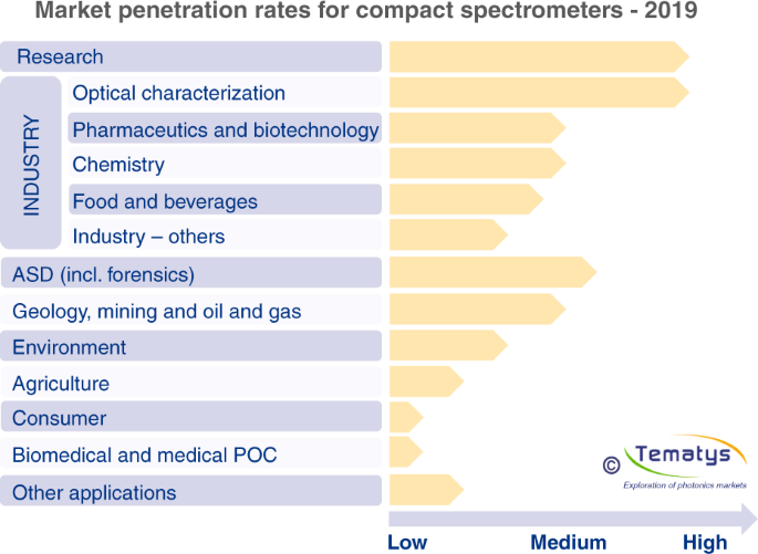
growth of the market volume of micro- and nano-spectrometers which arises from 655 million US dollars to 922 million in just three years between 2016 and 20199,25,26. The predicted
penetration rates and market values of compact spectrometers in different applications and segments are shown in Fig. 19. The research field has the largest value in 2019 whereas the rapid
growth occurs at consumer and biomedical markets almost from 300 to 400% within five years. Among those micro- and nano-spectrometers, chip-scale spectrometers are shown to play a dominant
role in the rapid market growth in coming years, due to their superior integrability into portable devices such as smartphones, wearable devices and drones, which, on the other hand, is the
main driving force behind the development of compact spectrometers. A recent report foresees that chip-scale spectrometers will have a disruptive increase in market volume from less than 2
million US dollars in 2019 to over 1.6 billion US dollars in 2024, as shown in Fig. 227. The rapidly expanding market imposes strong stimulations for both academia and industry players to
join this field. Hamamatsu launched a mini spectrometer with a size comparable to fingertip and a weight of only 0.3 g. The device works between 650 nm and 1050 nm with a spectral resolution
of about 15 nm, which is suitable for food inspection, light-level measurement and component analysis28. NeoSpectra-Micro developed an integrated near infrared spectral sensor (1250–2500
nm) with 16 nm resolution that can be used in a wide variety of material sensing applications for both qualitative and quantitative analysis29. Continuous efforts are also being poured into
developing low-cost chip-scale spectrometers that can be integrated into consumer electronics such as smartphones. For instance, Fraunhofer-ENAS announced its goal of batch producing “one
gram spectrometer” for smartphone integration at a cost of around one dollar10. Samsung patented their smartphone-embedded IR spectrometers and prepared to integrate them in Galaxy S11 for
skin moisture detection and CO2 measurement27. In 2020, trinamiX and Viavi Solutions had announced a joint force in building a near infrared spectrometer module targeting for consumer
devices. Very recently, Rockley Photonics, a silicon photonics enterprise focusing on telecommunications, released a whitepaper about highly manufacturable on-chip spectrometers for “clinic
on the wrist” health monitoring11. All these examples herald the rapid development of chip-scale spectrometers in the future, especially for the consumer and biomedical applications. It is
foreseeable that the next-generation integrated spectrometers will be developed on the basis of silicon photonics to enjoy massive productibility at low cost and targeted for the
adaptability in ecosystems of intelligent devices such as smartphone and wearable devices APPLICATION-ORIENTED ANALYSIS OF INTEGRATED SPECTROMETERS Chip-size integrated spectrometers offer
great potential for large-scale, in-field, and real-time spectroscopic sensing. Nevertheless, in general, the footprint reduction of a spectrometer consequentially give rise to certain
performance degradation regarding its operation bandwidth, resolution, measuring speed, dynamic range, or signal-to-noise ratio, making it crucial to customize the spectrometer design for
specified application scenarios. For example, in some cases such as the portable spectroscopies for chemical sensing, a resolution on the scale of 10 nm can be considered acceptable4, while
for the detection of biomarkers, such as blood glucose or lactate, a sub-nanometer resolution is desired to identify their wide signature absorption peaks (~30 nm) to ensure the measurement
accuracy30,31. Therefore, it is critical to establish a set of key figures and specify their application-oriented metrics. In this chapter, we discuss the application prospects for
integrated spectrometers in different fields, elaborating their key figures of merits in terms of resolution, bandwidth, etc. By now, the most popular but demanding application scenarios of
the integrated optical spectrometers include biomedical sensing for health monitoring and disease diagnosing, chemical sensing for pollution monitoring, gas leak detection and industrial
emission screening etc. These detections rely on different vibrational spectroscopies such as near-infrared (NIR, 700–2500 nm), mid-infrared (MIR, 2500–25,000 nm), and Raman spectroscopy
(2500–200,000 nm) techniques to measure the relevant markers30,31, i.e., to recognize certain chemical substances or functional groups based on the interaction between electromagnetic
radiation with vibrational molecules. Among them, since the MIR technique is not suitable for on-chip integration due to the lack of appropriate integration platforms (e.g., the transparency
windows for Si or SiN do not cover the broad MIR range), it is not within the scope of this paper. Here we focus on the NIR and Raman spectroscopy techniques that are applicable for
chip-size integrated spectrometers and summarize their key spectroscopic performance metrics required for different application scenarios. BIOMEDICAL SENSING The sensing of biomarkers in
either exhaled breath or biofluids, e.g., blood, breath, sweat, saliva, urine, is of great importance for bioanalysis and biomedical diagnosis32,33,34,35. For instance, the detection of the
glucose concentration in blood or saliva can provide diagnostic or monitoring information for diabetes, while measuring the electrolyte level in sweat helps screen for dehydration. These
biomedical measurements are commonly achieved by NIR spectroscopy techniques. Since the absorption bands in NIR region are prominently generated by a large number of overtones and
combinations of fundamental vibrations of -CH, -NH, and -OH functional groups, the information of various biomarkers can therefore be elucidated accordingly. Benefitting from the maturity of
spectrometer integration platform, NIR spectroscopy with portable devices has gradually become a research hotspot, showing promising prospects for in-vivo biomedical sensing. Figure 3
presents the absorption bands for typical functional groups of biological origins in the NIR range36. In theory, by identifying the spectral signatures at different bands, quantitative
information of corresponded chemical compounds can be retrieved, e.g., the overtones of -CH stretch are associated with carbohydrates while the overtones of -NH stretch relate to proteins.
However, given that these peaks in NIR region are rather broad and do overlap, specified spectrometer metrics, as well as additional calibration processes, such as partial least squares
regression (PLSR), are needed to extract the mixed bio-information with reasonable accuracy37,38. Specifically, such NIR spectrometers should be designed to feature high resolution in
particular wavelength regions where the minimum peak overlaps with water or other molecules exist, as well as high sensitivity since the measurable light (either reflected by or transmitted
through living tissues) is always rather weak. We first take the measurement of blood glucose as a representative example. As one of the earliest applications of NIR spectroscopy in medical
diagnosis, researchers have shown great interests in non-invasive systems for in-vivo blood glucose measurements to alleviate the pain and high cost of conventional invasive
methods38,39,40,41,42,43,44,45. The informative peaks of the glucose molecule come from the vibrations between -OH and -CH in either long wavelength-NIR (LW-NIR, 1300–2500 nm) or short
wavelength-NIR (SW-NIR, 700–1100 nm), representing the two main observe windows on which current analytical methods are based. Relatively, the spectral signatures in LW-NIR are more
pronounced than those in SW-NIR which enable higher precision for in-vitro measurement, while the absorption index in SW-NIR bands is notably lower, allowing a deeper penetration depth for
in-vivo testing. In Fig. 4, we summarize various reported in-vivo NIR-spectroscopy-based glucose sensing schemes indicating their target spectral bands and required spectrometer resolutions.
It can be seen that the SW-NIR based schemes normally require <300 nm bandwidths with sub-nanometer resolutions, while LW-NIR schemes need 300–1000 nm bandwidths with resolutions between
2 and 15 nm. Besides glucose, NIR spectroscopy has also been demonstrated to extract information about other metabolites, including lactate, urea, glutamine, Ammonia, and (de) oxygenated
hemoglobin etc.46,47,48,49,50,51,52. Since these compounds have lower concentrations in blood or cells compared to glucose, current measurement approaches are mostly based on in-vitro sample
testing, which rely on several hundreds of nanometers wide bandwidths with about 1 nm resolutions in the LW-NIR range. Note that in ref. 53, the detection of deoxygenated hemoglobin (Hb)
oxygenated hemoglobin (HbO2) applies only two wavelengths at 730 nm and 850 nm because the absorption spectra at these wavelengths differ significantly between Hb and HbO2, and the ratio is
then calculated to determine the concentrations. However, this measurement is not accurate on the patients with abnormal hemoglobin structure, abnormal hemoglobin levels. The above
performance requirements can already be met by some commercialized mini spectrometers but are still quite challenging for chip-scale integrated spectrometers. To realize wearable
non-invasive devices for in-vivo biomedical sensing, further evolvements in both instrumentation and spectral analysis algorithms are desired. INDUSTRIAL CHEMICAL DETECTION Besides
biomedical applications, optical spectroscopic sensing has also been proven as a versatile and powerful tool for high-efficiency industrial chemical detection of various substances. Among
them, NIR and Raman spectroscopy are widely adopted and are regarded as a couple of complementary techniques51. For instance, the strong infrared absorption of water (H2O) always severely
interferes the spectroscopic detection and limits the scope of applications whilst Raman spectroscopy is insensitive to water. Therefore, for chip-scale spectrometer, NIR and Raman (800~2500
nm) and their combination spectroscopies are well competent for realizing the high-efficiency chemical detection in a great variety of complicated industrial scenarios54,55,56,57,58,59.
Figure 5 indicates the spectrometer specifications for industrial chemical detection of solids, liquids and gases based on the NIR and Raman spectroscopy, respectively. The spectroscopic
sensing has been utilized to identify and quantify diverse solid, liquid and gas substances for pharmaceutical, agriculture, food, fuel, water pollution and atmospheric monitoring. Most of
the scenarios apply spectrometers with a resolution in a range from 0.1 nm to 10 nm. However, the resolution required for gas detection (pm-level) is almost three orders of magnitude higher
than that for solids and liquids (nm-level). Since molecules in the gaseous state rotate freely, the fine rotational structures can be observed in the form of fine absorption peaks,
especially occurring in the simple molecules (a group of atoms held together by covalent bonds)60. So far, the gas detection has been widely demanded by industrial applications, including
monitoring the hazardous gases for production safety management, detecting the emission of greenhouse gases and volatile organic compounds (VOCs) for environmental protection61. It can be
concluded that for industrial applications except agriculture and food analysis, it is always desirable for the spectrometers to have very high resolution (<1 nm) with a bandwidth over
100 nm, which, as mentioned above, remains a great challenge for integrated spectrometers at this moment. To summarize, the key spectroscopic requirements for both biomedical and industrial
chemical sensing applications are listed in Table 1, representing the goals that chip-size integrated spectrometers need to attain. In the following chapters, a variety of integrated
spectrometer technologies with diverse operating principles and architectures are discussed, including the state-of-the-art demonstrations and promising development directions. TECHNOLOGICAL
ANALYSIS OF INTEGRATED SPECTROMETERS From the perspective of fundamental technology route, the optical spectrometers can be roughly classified into two groups: wavelength de-multiplexing
based (WdM) and wavelength multiplexing (WM) based. As suggested by their names, the WdM spectrometers need to de-multiplex, or in other words, split the incident signals’ spectra, either
spatially or temporally, and measure the intensity of individual channel. On-chip WdM spectrometers are typically implemented by dispersive structures, in which different wavelengths exhibit
different propagation properties and consequently arrive at detectors distributed at different spatial locations or reach a single detector at different time. Alternatively, WdM
spectrometers can be implemented by using an array of narrowband filters or a single tunable narrowband filter, whose spectral responses determine the spectral contents arriving at the
detector, as shown in Fig. 6a, b. In contrast, WM spectrometers do not require to split the spectral contents of the spectrum, they typically pro-modulate the entire spectrum and reconstruct
it by signal processing using specific algorithms. Dependent on the modulation principle, they can be further divided into Fourier Transform Spectrometers (FTS), or Computational
Spectrometers (CS) as shown in Fig. 6c, d. Note that, in the figures, only the core parts of the integrated spectrometers are illustrated, which refer to the integrated optical elements that
are required to performance the spectrum reconstruction and are typically unique for different type of spectrometers. While a complete system of integrated spectrometer contains other
necessary auxiliary elements or devices, such as optical I/Os which couple light in and out of the chip, photodetectors (either on- of off-chip) that convert light to electrical signal for
post-processing, driving electronics, tuning elements and temperature controller. WDM SPECTROMETERS Being the most straightforward spectroscopic approach, integrated WdM spectrometers don’t
require complex computational sources, thus have attracted numerous research attention to be demonstrated on silicon photonics platform. Till now, gratings are the most widely adopted
elements for dispersive structures based WdM spectrometers. The fundamental principle is to create multi-path interference effects between the incident signal and make different wavelengths
arrive at different locations. Depending on how the multi-path interference is created, gratings based spectrometers can be further divided into planar concave grating (PCG) and arrayed
waveguide grating (AWG). PCG is the planar version of the classic diffraction grating spectrometer (such as Optical Spectrum Analyzer used in daily lab). The light enters from an input
aperture into the free propagation region (a slab waveguide section) after which it diffracts and hits the curved grating on the other end, which reflects as well as focuses different
wavelengths at different output apertures located along a so-called Rowland circle as shown in Fig. 7a, b. The spectral resolution is linearly dependent on the pitch of the output aperture
(spacing between two output waveguides) and inversely proportional to the Rowland radius that determines the device footprint as well as the group index of the material. Therefore,
demonstrating PCG on silicon photonics can offer significant reduction in footprint thanks to the high field confinement in the waveguide core that leads to a small output pitch and the
strong modal dispersion the generates a large group index. The first experimental demonstration on silicon photonics was in 2007 consisting of 4 channels with 20 nm channel spacing (i.e.,
spectral resolution) and a footprint of only 250 μm × 180 μm62. The main research focus since then have been given to improve the spectrometer’s performance by optimizing the gratings,
including using Bragg reflectors63,64 or photonics crystal reflectors65, coating grating with silver films66, Retro-reflecting V-shaped facets67. etc., as plotted in Fig. 7c–e. In contrast
with PCGs that use a slab waveguide section for the multi-path interference to take place, AWGs use an array of waveguides with varying lengths to create the multi-interference effect as
shown in Fig. 6a. Light enters from an input waveguide into a free space region and gets distributed among the imbalanced arrayed waveguides through in-plane diffraction. The phase shifts
contributed by the arrayed waveguides are wavelength dependent, consequently, the light coming out of the arrayed waveguides interfere in another free space region, such that different
wavelengths arrive at different output apertures. The length difference between the waveguide arms (delay length) relates directly to the Free Spectral Range (FSR) or the operation bandwidth
of the AWG, while at a given FSR, the spectral resolution can be simply improved by increasing the number of waveguides. The benefit of using silicon photonics as the platform for AWG lies
in the high confinement of light in the waveguide core, allowing tight bend radius and narrow waveguide spacing. In 1997, the first AWG on silicon photonics was demonstrated consisting of 4
channels spaced at 1.9 nm with a footprint of 2.7 cm × 2.7 cm40. Compared with PCG, AWG is relatively simpler in design and resolution improvement. However, it has larger footprint as it
incorporates two free propagation regions and an array of long waveguides. AWG is also more vulnerable to fabrication variations that induce phase errors along the arrayed waveguides, this
is why AWG typically exhibit stronger channel crosstalk than PCG. Various innovations have been created to combat those problems. For instance, the footprint reduction can be achieved by
replacing the free propagation regions with multi-mode interferometers (Fig. 8a)68 and connecting the ends of the arrayed waveguides to reflectors (Fig. 8b)69,70, while the crosstalk can be
suppressed by using advanced free propagation regions as well as wider waveguides, as shown in Fig. 8c, d71,72. This type of integrated spectrometers using PCG or AWG can perform single-shot
measurement as no tunning elements are present, thus the measurement speed can be fast. The system’s daynamic range is directly related with its operation bandwidth and resolution, as for
broader bandwidth and higher resolution, the incident light needs to be split into more ports, resulting in lower detected power at the detectors. The main limitation lies in the relatively
short propagation path compared with bulky system, which is the key factor toward high resolution, as longer waveguide length will inevitably bring more propagation loss and phase errors due
to fabrication imperfections, which in turn sacrifice the system’s dynamic range and reliability. As a consequence, the resolution of this type of integrated spectrometers is typically
limited to a few nm. Besides dispersive gratings, narrowband filters can also be developed toward WdM spectrometers. The most important advantage of filters based spectrometer over
dispersive gratings based spectrometer is the flexibility in tailoring the spectral response. For instance, by cascading Mach–Zehnder-Interferometers (MZIs) with varying armlength
differences, spectrometers with spectral resolutions from 0.13 nm to 20 nm can be easily synthesized73,74,75, as shown in Fig. 9a. By further optimizing the couplers in MZI, the spectrum of
each channel of the spectrometer can be tailored to flat-top instead of being Gaussian or Lorentzian shaped as those of dispersive gratings based spectrometers74, which is plotted in Fig.
9b. MZI is a non-resonant filter which intrinsically occupies large area, while using resonant filters such as ring resonators, Fabry-Perot etalons, photonics crystal cavities and Bragg
gratings can significantly reduce the linewidth as well as the footprint76,77,78. Fig. 9c shows a compact spectrometer consisting of 84 micro-donut resonators that could produce 0.6 nm
resolution within 50 nm operation bandwidth and only occupies a footprint of 200 μm × 50 μm79. 4 cascaded contra-coupled Bragg gratings can also achieve similar spectral responses compared
with the spectrometer consisting of over 10 cascaded MZIs but has a footprint that is one order of magnitude smaller80, as shown in Fig. 9d. Spectrometers based on narrowband filters array
have the advantages of single-shot measurement (fast measurement speed) as well as flexibility to tailor the resolution and bandwidth. Particularly for resonant filters, it can be easily
achieved ~10 pm resolution. But at the same time, they are vulnerable to fabrication variation that changes the operation wavelength as well as ambient environment fluctuations that can
induce instability of the operation wavelength. Also, they have similar problem with PCG or AWG based spectrometers that the dynamic range is directly related with operation bandwidth and
resolution. Another unique advantage of narrowband filter based spectrometer compared with dispersive gratings lies in the tunability of its operation wavelength, particularly for resonant
filters, which makes scanning spectrometer that uses a single filter with ultra-compact footprint and large dynamic range possible. However, for filters with very narrow linewidth (high
spectral resolution), tuning the wavelength for a broad optical range will require a significant amount of power consumption and the range will typically be limited by its free spectral
range. Therefore, the trend of combining dispersive gratings and narrowband filters for spectrometers with both broad bandwidth, high spectral resolution and small channel count is arising.
The dispersive gratings are intended to have low-resolution and split the spectrum into multiple channels with large bandwidth, while a narrowband filter finely scan each entire channel by
tuning its center wavelength. Recently, the combination of a AWG and ring resonators was demonstrated for 0.1 nm resolution and 25.4 nm bandwidth with only 9 channels as shown in Fig. 9e,
which is significantly reduced compared to a conventional AWG that would require 254 channels81. WM BASED SPECTROMETERS The fundamental principle of WdM spectrometers requires the spectrum
to be split into multiple channels, which limits the power at each detector and the dynamic range of the spectrometer. In contrast, WM spectrometers pre-process the entire spectrum of the
incident signal by certain type of modulation and reconstruct the spectrum using proper algorithms to post-process the modulated spectrum. Based on the specific modulation, WM based
spectrometers can be categorized as Fourier transform spectrometers (FTSs) and Computational spectrometers (CSs). FOURIER TRANSFORM SPECTROMETERS FTSs modulate the incident light via tuning
the optical path difference (OPD) to obtain the interferograms and then convert them back to the wavelength domain by performing Fourier transform in the post-processing stage, as shown in
Fig. 10a82. Compared with WdM spectrometers that commonly measure different spectral components separately in the temporal or spatial domain, the multiplexing measurement of FTSs can provide
much better SNR with higher optical throughput captured by the detectors, especially when the detector noise is dominant, which is identified as the Fellgett’s advantage (multiplex) and the
Jacquinot’s advantage (high optical throughput). According to the Rayleigh criterion, the spectral resolution δλ and bandwidth Δλ of FTSs are determined by the maximum OPD introduced to the
signal and the number of OPDs, respectively. For conventional free-spaced FTSs, the OPD modulation can be easily performed using a movable mirror as shown in Fig. 10a. While demonstrating
FTSs on integrated planar platform such as silicon photonics will require to identify approaches to implement variable OPD without mechanically moving parts. Depending on the mechanism of
introducing various OPD to the signal, FTSs demonstrated on silicon photonics can be further categorized into spatial heterodyne FTSs (SH-FTS) and temporal heterodyne FTSs (TH-FTS). SH-FTS
are based on a simple and stable multi-interferometer configuration composed of a spatial array of imbalanced MZIs, each of which produce a linearly increasing amount of OPD to the signal,
together they could produce a digitized interferogram of the input signal. This kind of configuration can easily produce a very large OPD that turns into high spectral resolution, but it
suffers from a similar problem with WdM based spectrometers: inherent trade-off between spectral performance (operation bandwidth, spectral resolution) and channel count. For example, the
demonstration in ref. 83 implements 32 MZIs for a resolution of 0.04 nm, but the bandwidth is limited to only 0.75 nm. The degree of polarization is exploited to further enhance its
performance at a given channel count. A Dual-polarization SH-FTS that can process both fundamental transverse electric and transverse magnetic modes was successfully demonstrated in 201915.
In detail, the dual-polarized SH-FTS is composed of MZIs with different waveguide widths and arm imbalances, where each MZI can contribute two sampling OPDs, one from the TE mode and the
other from the TM mode. As a consequence, the same number of MZIs can provide twice OPD compared with a single polarization operation, as shown in Fig. 10c. To further increase the spectral
performance of SH-FTS at a given channel count, advanced post-processing algorithms can be explored such as compressive sensing84 and machine learning85. The multi-interferometer
configuration with a single-aperture input allows the single-shot interference capture for rapid spectral measurement, while sacrificing the Jacquinot (throughput) advantage. Since the
incident light is required to be split equally into every MZI through tree-structured cascaded Y-junctions, the actual throughput for interference modulation at every OPD dramatically
decreases with the interferometer number. Temporal heterodyne FTS (TH-FTS), on the other hand, is more analogous to conventional free-space based FTS, as the OPDs are modulated in time
domain, and a single detector is used to capture the interferogram. The measurement time is sacrificed in order to maintain Jacquinot (throughput) advantage. Recently, two different
mechanisms of achieving temporal modulation of the OPD are demonstrated. First one is similar with SH-FTS in the sense that the OPDs are also in the form of varying physical length
difference, but optical switches are employed to dynamically change the physical pathway and realize the temporal modulation of OPD86, as shown in Fig. 10d. This approach indeed maintains
the Jacquinot (throughput) advantage while produces very high spectral resolution. But the optical switches impose limit on the operation bandwidth of the spectrometer. More importantly,
there will be always a leakage of signal that propagates along undesired pathway, leading to unwanted crosstalk when measuring interferograms at different OPDs, therefore introducing
difficulty in the post-processing. The second approach quasi-continuously modulate the OPD by taking advantage of thermos-optic effect to change the effective index of a fixed waveguide, as
shown in Fig. 10e. The challenge behind this approach mainly lies in the theoretical part dealing with various unwanted effects that only exist for waveguide structures, such as waveguide
dispersion that makes different spectral components experience different OPD, fabrication variation that causes two arms of the MZI unequal, thermal induced expansions that make waveguide
length varying when changing OPD etc. After successfully addressing this issues, the first experimental demonstration on silicon photonics was reported in 2018, with a bandwidth over 60 nm
and a spectral resolution of only 3 nm16. After that, the research attention has been given to further increase its resolution. The fundamental reasons for this low resolution include short
waveguide length and low power injection to the heater. Increasing waveguide length will result in large propagation loss and high electrical resistance for the heater. By using advanced
waveguide design to reduce the optical loss as well as heater structures to receive higher power injection, Li et al. successfully increase the waveguide length from 3 cm in ref. 16 to 10 cm
in ref. 87, and the spectral resolution is increased to sub-nanometer. Later, Li et al. combines multiple techniques to further increase the resolution to 0.16 nm, including Michelson
interferometers (MI) structure to double the OPD, an optimized heater and air trenches to achieve higher thermal efficiency, a novel multiple interferometers approach is employed which
combines balanced MI with N statically imbalanced MIs, thereby increasing the OPD of a single MI by factor of N + 1, as shown in Fig. 10f17. COMPUTATIONAL SPECTROMETERS Recently, a new
scheme of WM based spectrometer named computational spectrometer has drawn extensive study, which utilizes an array of propagation channels with distinct spectral responses, each of which
can be interpreted as sampling coefficients of the incident spectrum at each wavelength point, as shown in Fig. 11a. Therefore, each channel can sample the entire spectrum simultaneously.
The incident spectrum can be accurately reconstructed using advanced algorithms to process the sampled results of all channels. In contrast, each channel (filter) of narrowband filters based
spectrometers only samples the incident spectrum at a specific wavelength point or a small band equivalent with spectral resolution. Consequently, no advanced signal post-processing is
required, but the number of channels (filters) must equal the ratio of operation bandwidth and spectral resolution. While for computational spectrometers, with proper engineering of
channels’ spectral responses, the number of channels can be drastically reduced, leading to a significant improvement upon footprint and dynamic range at same bandwidth and resolution. The
principle can also be mathematically explained. When a signal with a spectrum Φ(λ) propagates through a channel with spectral response F(λ) and gets detected by a photodetector, the output
current is $${{{\mathrm{I}}}} = {{{\mathrm{A}}}}{\int}_{\lambda _1}^{\lambda _M} {{{{\mathrm{F}}}}(\lambda )\Phi (\lambda ){{{\mathrm{d}}}}\lambda }$$ where A represents the link loss
including the responsibility of the detector, λ1 and λM refer to the starting and ending wavelength of the spectrum, respectively. For signal processing purpose, the equation can be
discretized as $${{{\mathrm{I}}}} = {{{\mathrm{AF}}}}_{1xM}\Phi _{Mx1}$$ Similarly, if the signal passes through N channels with distinct F, the equation has the form of
$${{{\mathrm{I}}}}_{Nx1} = {{{\mathrm{AF}}}}_{NxM}\Phi _{Mx1}$$ For narrowband filters based spectrometer, F is a matrix with only one nonzero component at each row, thus the equation can
only be solved when N = M. While for computational spectrometers, with advanced algorithms and proper FNxM, this equation can still be reasonably solved at the case N ≪ M, obeying the
following rule: $$minimize \, \left| {\left| {I - AF\Phi } \right|} \right|_2 \,+\, \alpha \left| {\left| {{{\Gamma }}\Phi } \right|} \right|_{{{\mathrm{2}}}} \,
{{{\mathrm{subject}}}}\,{{{\mathrm{to}}}}\,0 \le \Phi \le 1$$ where α represents the coefficient of the regularization term that helps smoothen the spectrum and Γ is a matrix helping
calculate the derivative of Φ, which is used for regularization purpose. At a fixed channel number (typically limited by footprint and/or SNR), the channel spectral responses will influence
the quality of spectrum reconstruction significantly. Using this concept for reconstructing signals in a specific domain is not novel. Back in 1987, researchers already proposed to design a
velocimeter (a device reconstructing velocities) using random patterns88. In 1997 a holographic-sensor was designed using random gratings89. Applying this concept in signal acquisition and
imaging processing has also been a well-established technique starting from early of 2000, identified as compressed sensing90. In the field of optical spectrometer, this concept was
originally adopted only to combat with the non-ideality of narrowband filters91,92,93,94. In other words, these spectrometers still consist of narrowband filters, but optical span outside
filters’ passbands is not zero due to fabrication imperfections, causing unwanted sampling at other wavelength span. Only till 2013, researchers theoretically verified the possibility to
employ intentionally designed filters with random transmittances for improving spectrometer’s performance, as shown in Fig. 11b95. The main efforts since then have been put to find
integrated filters or dispersive media with desirable spectral responses in order to provide good performance (large M) with only a small number of channels (small N). Generally speaking,
the channel spectral responses should meet following requirements: * Each channel’s spectral response should be linearly independent with the others to provide uncorrelated spectrum
sampling. * Each channel’s spectral response should contain adequate sharp features to provide high sampling resolution as the minimum optical distance between two distinguishable points in
the spectral response determines the spectral resolution of this filter. * The channels should be compact, low loss and be able to enjoy massive production. It is nontrivial to get an array
of filters that meet those requirements simultaneously. The first demonstration on silicon photonics was based on random media with numerous air holes distributed in the light propagation
area as shown in Fig. 11c13. Thanks to its high level of randomness, the first two requirements were met and the spectrometer with about 30 channels can produce a spectral resolution of 0.75
nm within 25 nm bandwidth. The use of silicon photonics indeed enables massive production for such spectrometer, but the large amount of air holes introduces significant loss to the signal
(as evident in Fig. 11c, most of the light scattered outside before arriving at the detectors), which makes it impossible to be used in power-sensitive applications like wearable devices for
glucose and lactic acid monitoring. Also 25 nm bandwidth is inadequate for most health monitoring devices. On the other hand, researchers explore interferences instead of scatterings to
create physical channels with distinct spectral responses to minimize the optical loss. An ultra-long multimode silicon waveguide with a spiral shape was developed toward computational
spectrometer in 2016, plotted in Fig. 11d96. The interference between the modes in the waveguide as well as the intentional evanescent coupling between neighboring arms of the spiral
contribute to a random spectral response at each detector. The resolution is reported to be as high as 0.01 nm but the bandwidth is relatively limited due to the very sharp speckles in the
spectral responses. Moreover, the waveguide length has to be very long in order to provide rich interference patterns, which inevitably increase the device’s footprint and optical loss. Very
recently, a novel computational spectrometer utilizes an array of stratified waveguide filters with distinct spectral responses was demonstrated20,97. The stratified waveguide filter
combines the random medium theory and low-loss silicon strip waveguide to produce distinct spectral response but suppress scattering loss induced by random medium as shown in Fig. 11e. Only
32 channels were adequate to produce a bandwidth of 180 nm and a resolution of 0.45 nm. Even if the computational spectrometers exhibit distinct advantages in terms of footprint, dynamic
range and measurement time, but the nature of using much less equations to solve many unknown values determines it is only good to reconstruct sparse spectra, which refer to smooth spectra
or spectra with only a few nonzero components. While for dense spectra that contain rapidly changing features such a series of dips and peaks, the number of filters have to been
significantly increased in order to maintain satisfying performance. In this chapter, we review the mainstream approaches toward integrated spectrometers on silicon photonics. For summary,
we present the general characteristics for different types of integrated spectrometers in Table 2. OUTLOOK As discussed above, due to strong demand from practical applications such as
biomedical sensing and industrial detection, developing integrated spectrometers with sufficient performance and massive manufacturability has never been so imperative. To date, silicon
photonics is still the most promising platform due to its unique CMOS compatibility. Considering that currently demonstrated integrated spectrometers are still unsatisfiable to the market
requirements, we foresee four possible directions for developing the next-generation spectrometers on silicon photonics: ACTIVE PATH SCANNING COMPUTATIONAL SPECTROMETERS The rapidly growing
consumer market in biomedical and chemical sensing applications have placed high spectroscopic requirements, including broad bandwidth, high resolution, and large dynamic range. However, no
integrated spectrometer has so far accomplished all these merits due to respective limitations. For instance, in order to achieve broad bandwidth and high resolution, a large number of
splitting channels is required for dispersive gratings, narrowband filters and SH-FTS spectrometers, which inevitably degrade the system’s dynamic range. TH-FTS doesn’t require to split the
signal and can enjoy large dynamic range, but it requires a large amount of power consumption (>5 W) for sub-nm resolution, which is unacceptable for consumer electronics. Computational
spectrometers are believed promising for achieving a balanced performance with compact footprint and low power consumption, as it can significantly reduce the number of channels compared
with dispersive gratings or narrowband filters based spectrometer, and do not demand power consumption compared with tunable filters spectrometers or TH-FTS. But current demonstrations still
require the incident signal to be split over 30~50 sampling channels and the channel count has to scale up in order to achieve better performance, which reduces the power intensity in each
channel, resulting in a worse SNR and smaller dynamic range. One potential solution is to replace the passive optical power splitting with active path scanning, that is, to actively
configure different optical paths (sampling channels) for the incident signal over time, rather than splitting it over space, as shown in Fig. 12a. Consequently, a single detector is
adequate to reconstruct the incident spectrum, leading to a large dynamic range for the spectrometer. Such reconfigurable switching network can be easily scaled up with exponentially
increasing channel numbers to support ultra-high resolution, though at the cost of larger footprint, higher power consumption, and more complex driving circuits. Since the mainstream
thermo-optic or electro-optic based optical switch technologies can achieve at least microsecond scale switching time98,99, the total detection time for such path-reconfigurable spectrometer
can be within one second even for hundreds of detection channels. SPECTROMETER WITH PROGRAMMABILITY Currently demonstrated spectrometers, irrespective of platforms and working principles,
are all fixed in terms of performance, such as the center wavelength, operation bandwidth and spectral resolution. While it is highly desirable to develop a universal spectrometer that can
dynamically tune its performance in order to suit requirements of different applications or working scenarios. Ideally, all of the spectrometers’ performance indicators are desired to be
programmable, while in practice, it would be valuable enough to develop a spectrometer with adjustable bandwidth and resolution. This idea can be possibly realized in incorporation with
programmable photonic integrated circuits (PICs)100,101, which is an emerging technology allowing the on-chip optical signal to be manipulated at run-time to enable various applications. As
shown in Fig. 12b, a reconfigurable PIC-based spectrometer system can be established with arrayed modules which include different components such as Mach–Zehnder interferometers, ring
resonators, photon detectors, and etc. By dynamically configuring the interconnections between the modules, the spectrometer architectures can be tailored for different application
scenarios, e.g., the resolution can be adjusted by selecting different filter arrays. Similarly, though with sacrifices in device size and power comsuption, such designs could bring wide
flexibility and versatility in practical applications. PARALLELISM IN SPECTROMETER SYSTEM Parallelism, which has always existed in the design of optical transmission system since the arise
of wavelength division multiplexing (WdM) technologies102,103, can also be explored to enhance spectrometer’s performance. Currently, WdM is widely adopted for on-chip optical communication
to increase the data volume and has been proved to be able to cover a broad bandwidth, such as C+L-band WdM104 and O+C-band WdM105. Analogically, parallelism can also be introduced into the
design of spectrometer systems as shown in Fig. 12c, e.g., as a single integrated spectrometer may suffer from its limited bandwidth, by parallelly implementing a spectrometer array with
different operating spectral ranges, the combined bandwidth can be significantly increased. More specifically, for applications, such as the NIR bio-sensing where various signature peaks at
some specific wavelengths are to be detected, it is not realistic and also cost-worthy to build an ultra-broadband spectrometer that covers the whole spectral range with high resolution.
Instead, the NIR incident signal can be firstly demultiplexed into multiple target bands (with those unwanted bands abandoned) and then detected by different spectrometers, respectively.
Unlike the spatial power splitting which harms the signal intensity, the wavelength demultiplexing process does not affect the signal quality. In addition, the spectrometers targeted for
different bands can be customized to match the practical performance requirements at that band. Again, such spectrometer systems will inevitably be more complicated and require more building
blocks than a single spectrometer but are still highly feasible for low-cost massive production thanks to the advances in large-scale photonic integration techniques106,107. HYBRID
PLATFORMS FOR SPECTROMETERS Besides the design of spectrometer system itself, to realize full functionalities, it is desired to also implement high-performance light sources and photon
detectors within the same chip package, which requires the introduction of other materials on the basis of silicon photonics. Currently, the mainstream integrated photodetectors are based on
germanium, as it’s already a standard fabrication process in many CMOS foundries. However, Ge-on-Si photon detectors always suffer from high dark currents and low absorptivity attributed to
its nature of indirect bandgap, and normally cannot cover the spectral range beyond NIR108,109. III-V materials, in contrast, feature direct and tunable bandgap, thus can achieve high
absorption coefficients at different spectral bands. Moreover, they can also serve as gain materials for optical emitters, such as lasers110 or LEDs111. Currently, high-density
cost-efficient III-V-on-Silicon integration relies on hybrid integration approaches, such as, flip-chip bonding112, die/wafer-to-wafer bonding113, and micro-transfer printing114. Therefore,
it is predictable that hybrid integrated platforms will play an important role in the future commercialization of integrated spectrometers. Beyond silicon photonic platforms, polymer-based
3D lithography offers new possibilities for massive producible miniaturized spectrometers. Based on the laser-induced polymerization effect, current commercial 3D nano printer can implement
arbitrary three-dimensional pattern with <200 nm feature size. A variety of demonstrations of 3D-nanoprinted spectrometers have been reported based on different principles ranging from
free-space optics to computational reconsctruction115,116. An additional design dimension could bring unique advantages for 3D nano-printed spectrometers, such as ultra-compact footprint. A
wide operation bandwidth can also be expected thanks to the various ultra-broadband 3D optical coupling strategies117. However, at current stage, 3D nano printing only supports passive
polymer structures, making external light sources and photo detectors indispensable. Therefore, by implanting the 3D nano-printed spectrometer onto the hybrid integrated III-V-on-Silicon
PICs, it is possible to enjoy the advantages from both sides, representing a promising development direction. CONCLUSION With the rapid development of Internet-of-Things and popularity of
intelligent portable device, the demand for low-cost, lightweight, miniaturized spectrometers has never been so imperative. Various efforts have been made to miniaturize spectrometers, yet
they somewhat lack technological readiness for commercial products. Being compatible with CMOS technology, silicon photonics is widely accepted to be one of the most promising platforms for
mass-manufacturable photonic integrated circuits. Therefore, in this paper we review recent progresses in integrated spectrometers that leverage silicon photonics technology, including their
market trends, application-oriented requirements with a special focus on biomedical sensing and industrial detections, and technological evolution that covers mainstream structures for
silicon integrated spectrometers. Four possible research directions are foreseen for developing next-generation integrated spectrometers. We expect to see expanding integration of chip-scale
spectrometers into consumer productions within the next few years, providing cost-effective and reliable services to users worldwide. REFERENCES * Savage, N. Spectrometers. _Nat. Photonics_
3, 601–602 (2009). Article ADS Google Scholar * Bacon, C. P., Mattley, Y. & DeFrece, R. Miniature spectroscopic instrumentation: applications to biology and chemistry. _Rev. Sci.
Instrum._ 75, 1–16 (2004). Article ADS Google Scholar * Chow, A. W. Lab-on-a-chip: opportunities for chemical engineering. _AIChE J._ 48, 1590–1595 (2002). Article Google Scholar *
Crocombe, R. A. Portable spectroscopy. _Appl. Spectrosc._ 72, 1701–1751 (2018). Article ADS Google Scholar * McGonigle, A. J. S. et al. Smartphone spectrometers. _Sensors_ 18, 223 (2018).
Article ADS Google Scholar * Hakala, T. et al. Direct reflectance measurements from drones: sensor absolute radiometric calibration and system tests for forest reflectance
characterization. _Sensors_ 18, 1417 (2018). Article ADS Google Scholar * Blind, N. et al. Spectrographs for astrophotonics. _Opt. Express_ 25, 27341–27369 (2017). Article ADS Google
Scholar * He, Z. P., Shu, R. & Wang, J. Y. Imaging spectrometer based on AOTF and its prospects in deep-space exploration application. In _Proceedings of SPIE 8196, International
Symposium on Photoelectronic Detection and Imaging_ (SPIE, Beijing, 2011). * Kulakowski, J. & d’Humières, B. Chip-size spectrometers drive spectroscopy towards consumer and medical
applications. In _Proceedings of SPIE 11693, Photonic Instrumentation Engineering VIII_ (SPIE, 2021). * Fraunhofer. _Miniature spectrometer for the smartphone_ (Fraunhofer-Gesellschaft,
2021). https://www.fraunhofer.de/en/press/research-news/2021/july-2021/miniature-spectrometer-for-the-smartphone.html. * Rockley Photonics. Real-time, non-invasive biomarker sensing on the
wrist. https://rockleyphotonics.com/wp-content/uploads/2021/07/Rockley-Photonics-Biomarker-Sensing-on-the-Wrist.pdf (2021). * Yang, Z. Y. et al. Miniaturization of optical spectrometers.
_Science_ 371, eabe0722 (2021). Article ADS Google Scholar * Redding, B. et al. Compact spectrometer based on a disordered photonic chip. _Nat. Photonics_ 7, 746–751 (2013). Article ADS
Google Scholar * Yang, Z. Y. et al. Single-nanowire spectrometers. _Science_ 365, 1017–1020 (2019). Article ADS Google Scholar * Wang, H. J. et al. On-chip Fourier transform
spectrometers by dual-polarized detection. _Opt. Lett._ 44, 2923–2926 (2019). Article ADS Google Scholar * Souza, M. C. M. M. et al. Fourier transform spectrometer on silicon with
thermo-optic non-linearity and dispersion correction. _Nat. Commun._ 9, 665 (2018). Article ADS Google Scholar * Li, A. & Fainman, Y. Integrated silicon Fourier transform spectrometer
with broad bandwidth and ultra-high resolution. _Laser Photonics Rev._ 15, 2000358 (2021). Article ADS Google Scholar * Bao, J. & Bawendi, M. G. A colloidal quantum dot spectrometer.
_Nature_ 523, 60–70 (2015). Article ADS Google Scholar * Zhu, X. X. et al. Broadband perovskite quantum dot spectrometer beyond human visual resolution. _Light.: Sci. Appl._ 9, 73
(2020). Article ADS Google Scholar * Li, A. & Fainman, Y. On-chip spectrometers using stratified waveguide filters. _Nat. Commun._ 12, 2704 (2021). Article ADS Google Scholar *
Soref, R. The past, present, and future of silicon photonics. _IEEE J. Sel. Top. Quantum Electron._ 12, 1678–1687 (2006). Article ADS Google Scholar * Khan, S. et al. Silicon-on-nitride
waveguides for mid- and near-infrared integrated photonics. _Appl. Phys. Lett._ 102, 121104 (2013). Article ADS Google Scholar * Yang, H. J. et al. Transfer-printed stacked nanomembrane
lasers on silicon. _Nat. Photonics_ 6, 615–620 (2012). Article ADS Google Scholar * Chen, S. M. Electrically pumped continuous-wave III–V quantum dot lasers on silicon. _Nat. Photonics_
10, 307–311 (2016). Article ADS Google Scholar * Kulakowski, J. & d’Humières, B. Compact spectrometers: technologies, market trends and needs. _PhotonicsViews_ 18, 28–30 (2021).
Article Google Scholar * High sensitivity in the near infrared region (to 1050 nm), ultra-compact grating type spectrometer.
https://www.hamamatsu.com/eu/en/product/type/C14384MA-01/index.html (2019). * Kulakowski, J. & d’Humières, B. _Miniature, micro and chip-size spectrometers: technologies, market trends
and customers’ needs_ (Tematys, 2020). * NeoSpectra-Micro spectral FT-IR sensor. https://www.photonicsolutions.co.uk/product-detail.php?prod=6815 (2022). * Ikoba, J. J. Samsung patents a
smartphone-embedded IR Spectrometer; could be on the Galaxy S11. https://www.gizmochina.com/2019/10/01/samsung-patents-a-smartphone-embedded-ir-spectrometer-could-be-on-the-galaxy-s11/
(2019). * Malin, S. F. et al. Noninvasive prediction of glucose by near-infrared diffuse reflectance spectroscopy. _Clin. Chem._ 45, 1651–1658 (1999). Article ADS Google Scholar *
Uwadaira, Y. et al. Development of a non-invasive blood glucose sensor using short-wavelength near-infrared spectroscopy and its application to glycemic index determination. _Nippon Shokuhin
Kagaku Kogaku Kaishi_ 58, 97–104 (2011). Article Google Scholar * Ahn, H. et al. Emerging optical spectroscopy techniques for biomedical applications—a brief review of recent progress.
_Appl. Spectrosc. Rev._ 53, 264–278 (2018). Article ADS Google Scholar * Parachalil, D. R. et al. Analysis of bodily fluids using vibrational spectroscopy: a direct comparison of Raman
scattering and infrared absorption techniques for the case of glucose in blood serum. _Analyst_ 144, 3334–3346 (2019). Article ADS Google Scholar * Zhou, X. Y. et al. Nanomaterial-based
gas sensors used for breath diagnosis. _J. Mater. Chem. B_ 8, 3231–3248 (2020). Article Google Scholar * Metrohm NIRSystems. _A guide to near-infrared spectroscopic analysis of industrial
manufacturing processes_ (Spring, 2013). * Türker-Kaya, S. & Huck, C. W. A review of mid-infrared and near-infrared imaging: principles, concepts and applications in plant tissue
analysis. _Molecules_ 22, 168 (2017). Article Google Scholar * Henn, R. et al. Hemodialysis monitoring using mid- and near-infrared spectroscopy with partial least squares regression. _J.
Biophotonics_ 11, e201700365 (2018). Article Google Scholar * Uwadaira, Y. et al. Identification of informative bands in the short-wavelength NIR region for non-invasive blood glucose
measurement. _Biomed. Opt. Express_ 7, 2729–2737 (2016). Article Google Scholar * Xue, J. T. et al. Noninvasive and fast measurement of blood glucose in vivo by near infrared (NIR)
spectroscopy. _Spectrochimica Acta Part A Mol. Biomolecular Spectrosc._ 179, 250–254 (2017). Article Google Scholar * Heise, H. M. et al. Noninvasive blood glucose sensors based on
near-infrared spectroscopy. _Artif. Organs_ 18, 439–447 (1994). Article Google Scholar * Burmeister, J. J., Arnold, M. A. & Small, G. W. Noninvasive blood glucose measurements by
near-infrared transmission spectroscopy across human tongues. _Diabetes Technol. Therapeutics_ 2, 5–16 (2004). Article Google Scholar * Xu, K. X. et al. Non-invasive glucose sensing with
near-infrared spectroscopy enhanced by optical measurement conditions reproduction technique. _Opt. Lasers Eng._ 43, 1096–1106 (2005). Article Google Scholar * Zuo, P. et al. Analysis of
noninvasive measurement of human blood glucose with ANN-NIR spectroscopy. In _Proceedings of 2005 international conference on neural networks and brain_ (IEEE, Beijing, 2005), 1350–1353. *
Brown, C. D. et al. Clinical assessment of near-infrared spectroscopy for noninvasive diabetes screening. _Diabetes Technol. Therapeutics_ 7, 456–466 (2005). Article Google Scholar *
Guevara, E. & Gonzalez, F. J. Joint optical-electrical technique for noninvasive glucose monitoring. _Rev. Mexicana De. F.íSci._ 56, 430–434 (2010). Google Scholar * Lafrance, D.,
Lands, L. C. & Burns, D. H. Measurement of lactate in whole human blood with near-infrared transmission spectroscopy. _Talanta_ 60, 635–641 (2003). Article Google Scholar * Lafrance,
D., Lands, L. C. & Burns, D. H. In vivo lactate measurement in human tissue by near-infrared diffuse reflectance spectroscopy. _Vibrational Spectrosc._ 36, 195–202 (2004). Article
Google Scholar * Ramasahayam, S. & Chowdhury, S. R. Non invasive estimation of blood urea concentration using near infrared spectroscopy. _Int. J. Smart Sens. Intell. Syst._ 9, 449–467
(2016). Google Scholar * Eddy, C. V. & Arnold, M. A. Near-infrared spectroscopy for measuring urea in hemodialysis fluids. _Clin. Chem._ 47, 1279–1286 (2001). Article Google Scholar *
Chung, H. et al. Simultaneous measurement of glucose and glutamine in aqueous solutions by near infrared spectroscopy. _Appl. Biochem. Biotechnol._ 50, 109–125 (1995). Article Google
Scholar * Rhiel, M. et al. Nondestructive near-infrared spectroscopic measurement of multiple analytes in undiluted samples of serum-based cell culture media. _Biotechnol. Bioeng._ 77,
73–82 (2002). Article Google Scholar * Cao, N. & Gao, T. X. Noninvasive tissue blood oxygenation measurement based on near infrared spectroscopy (NIRS). In _Proceedings of the 2009 3rd
International Conference on Bioinformatics and Biomedical Engineering_ (IEEE, Beijing, 2009), 1–4. https://doi.org/10.1109/ICBBE.2009.5163118. * Ayaz, H. et al. Early diagnosis of traumatic
intracranial hematomas. _J. Biomed. Opt._ 24, 051411 (2019). Article ADS Google Scholar * Doddridge, G. D. & Shi, Z. Q. Multivariate figures of merit (FOM) investigation on the
effect of instrument parameters on a Fourier transform-near infrared spectroscopy (FT-NIRS) based content uniformity method on core tablets. _J. Pharm. Biomed. Anal._ 102, 535–543 (2015).
Article Google Scholar * Wiercigroch, E. et al. Raman and infrared spectroscopy of carbohydrates: a review. _Spectrochimica Acta Part A Mol. Biomolecular Spectrosc._ 185, 317–335 (2017).
Article ADS Google Scholar * Wang, H. J. et al. Note: a unibody NIR transmission probe for in situ liquid detection. _Rev. Sci. Instrum._ 89, 036104 (2018). Article ADS Google Scholar
* Li, M. G. et al. Data fusion of Raman and near-infrared spectroscopies for the rapid quantitative analysis of methanol content in methanol–gasoline. _Energy Fuels_ 33, 12286–12294 (2019).
Article Google Scholar * Cabernard, L. et al. Comparison of Raman and Fourier transform infrared spectroscopy for the quantification of microplastics in the aquatic environment. _Environ.
Sci. Technol._ 52, 13279–13288 (2018). Article ADS Google Scholar * Cossel, K. C. et al. Open-path dual-comb spectroscopy to an airborne retroreflector. _Optica_ 4, 724–728 (2017).
Article ADS Google Scholar * Campanella, B., Palleschi, V. & Legnaioli, S. Introduction to vibrational spectroscopies. _ChemTexts_ 7, 5 (2021). Article Google Scholar * Khan, S., Le
Calvé, S. & Newport, D. A review of optical interferometry techniques for VOC detection. _Sens. Actuators A: Phys._ 302, 111782 (2020). Article Google Scholar * Brouckaert, J. et al.
Planar concave grating demultiplexer fabricated on a nanophotonic silicon-on-insulator platform. _J. Lightwave Technol._ 25, 1269–1275 (2007). Article ADS Google Scholar * Pottier, P.,
Strain, M. J. & Packirisamy, M. Integrated microspectrometer with elliptical Bragg mirror enhanced diffraction grating on silicon on insulator. _ACS Photonics_ 1, 430–436 (2014). Article
Google Scholar * Muneeb, M. et al. Demonstration of Silicon-on-insulator mid-infrared spectrometers operating at 3.8 μm. _Opt. Express_ 21, 11659–11669 (2013). Article ADS Google
Scholar * Momeni, B. et al. An on-chip silicon grating spectrometer using a photonic crystal reflector. _J. Opt._ 12, 035501 (2010). Article ADS Google Scholar * Xie, S. J. et al.
Silicon nitride/silicon dioxide echelle grating spectrometer for operation near 1.55 μm. _IEEE Photonics J._ 10, 4502207 (2018). Article Google Scholar * Brouckaert, J. et al. Planar
concave grating demultiplexer with high reflective Bragg reflector facets. _IEEE Photonics Technol. Lett._ 20, 309–311 (2008). Article ADS Google Scholar * Taha, A. M. et al. Compact
MMI-based AWGs in a scalable monolithic silicon photonics platform. _IEEE Photonics J._ 13, 6600306 (2021). Article Google Scholar * Dai, D. X. et al. Experimental demonstration of an
ultracompact Si-nanowire-based reflective arrayed-waveguide grating (de)multiplexer with photonic crystal reflectors. _Opt. Lett._ 35, 2594–2596 (2010). Article ADS Google Scholar * Fang,
Q. et al. Folded silicon-photonics arrayed waveguide grating integrated with loop-mirror reflectors. _IEEE Photonics J._ 10, 4900508 (2018). Article Google Scholar * Tondini, S. et al.
Methods for low crosstalk and wavelength tunability in arrayed-waveguide grating for on-silicon optical network. _J. Lightwave Technol._ 35, 5134–5141 (2017). Article ADS Google Scholar *
Pathak, S. et al. Comparison of AWGs and echelle gratings for wavelength division multiplexing on silicon-on-insulator. _IEEE Photonics J._ 6, 4900109 (2014). Article Google Scholar *
Munk, D. et al. Eight-channel silicon-photonic wavelength division multiplexer with 17 GHz spacing. _IEEE J. Sel. Top. Quantum Electron._ 25, 8300310 (2019). Article Google Scholar * Xu,
H. N. & Shi, Y. C. Flat-top CWdM (de)multiplexer based on MZI with bent directional couplers. _IEEE Photonics Technol. Lett._ 30, 169–172 (2018). Article ADS Google Scholar * Davis,
J. A. et al. Novel spectral-shaping building block: a narrowband Mach-Zehnder interferometer. _Photonics Res._ 8, 1059–1063 (2020). Article Google Scholar * Li, A. & Bogaerts, W.
Experimental demonstration of a single silicon ring resonator with an ultra-wide FSR and tuning range. _Opt. Lett._ 42, 4986–4989 (2017). Article ADS Google Scholar * Li, A. &
Bogaerts, W. Using backscattering and backcoupling in silicon ring resonators as a new degree of design freedom. _Laser Photonics Rev._ 13, 1800244 (2019). Article Google Scholar * Li, A.
et al. Backscattering in silicon microring resonators: a quantitative analysis. _Laser Photonics Rev._ 10, 420–431 (2016). Article ADS Google Scholar * Xia, Z. X. et al. High resolution
on-chip spectroscopy based on miniaturized microdonut resonators. _Opt. Express_ 19, 12356–12364 (2011). Article ADS Google Scholar * Shi, W. et al. Ultra-compact, flat-top demultiplexer
using anti-reflection contra-directional couplers for CWDM networks on silicon. _Opt. Express_ 21, 6733–6738 (2013). Article ADS Google Scholar * Zheng, S. N. et al. A single-chip
integrated spectrometer via tunable microring resonator array. _IEEE Photonics J._ 11, 6602809 (2019). Article Google Scholar * Faix, O. Fourier transform infrared spectroscopy. In
_Methods in Lignin Chemistry_ (eds. Lin, S. Y. & Dence, C. W.) 83–109 (Berlin: Springer, 1992). * Velasco, A. V. et al. High-resolution Fourier-transform spectrometer chip with
microphotonic silicon spiral waveguides. _Opt. Lett._ 38, 706–708 (2013). Article ADS Google Scholar * Podmore, H. et al. Demonstration of a compressive-sensing Fourier-transform on-chip
spectrometer. _Opt. Lett._ 42, 1440–1443 (2017). Article ADS Google Scholar * Herrero-Bermello, A. et al. On-chip Fourier-transform spectrometers and machine learning: a new route to
smart photonic sensors. _Opt. Lett._ 44, 5840–5843 (2019). Article ADS Google Scholar * Li, A. et al. Fabrication-tolerant Fourier transform spectrometer on silicon with broad bandwidth
and high resolution. _Photonics Res._ 8, 219–224 (2020). Article Google Scholar * Oliver, J., Lee, W. B. & Lee, H. N. Filters with random transmittance for improving resolution in
filter-array-based spectrometers. _Opt. Express_ 21, 3969–3989 (2013). Article ADS Google Scholar * Aizu, Y., Ogino, K. & Asakura, T. A laser velocimeter using a random pattern. _Opt.
Commun._ 64, 205–210 (1987). Article ADS Google Scholar * Ojeda-Castañeda, J. & Sauceda, A. Random gratings as correlator sensors. _Opt. Lett._ 22, 257–258 (1997). Article ADS
Google Scholar * Donoho, D. L. Compressed sensing. _IEEE Trans. Inf. Theory_ 52, 1289–1306 (2006). Article MathSciNet MATH Google Scholar * Oliver, J. et al. Improving resolution of
miniature spectrometers by exploiting sparse nature of signals. _Opt. Express_ 20, 2613–2625 (2012). Article ADS Google Scholar * Chang, C. C. et al. Spectrum reconstruction for
filter-array spectrum sensor from sparse template selection. _Optical Eng._ 50, 114402 (2011). Article ADS Google Scholar * Kurokawa, U., Choi, B. I. & Chang, C. C. Filter-based
miniature spectrometers: spectrum reconstruction using adaptive regularization. _IEEE Sens. J._ 11, 1556–1563 (2011). Article ADS Google Scholar * Chang, C. C. & Lee, H. N. On the
estimation of target spectrum for filter-array based spectrometers. _Opt. Express_ 16, 1056–1061 (2008). Article ADS Google Scholar * Li, A. et al. Ultra-compact single-shot spectrometer
enabled by stratified waveguide filters. In _Proceedings of the 26th Optoelectronics and Communications Conference_ (OSA, Hong Kong, China, 2021). * Redding, B. et al. Evanescently coupled
multimode spiral spectrometer. _Optica_ 3, 956–962 (2016). Article ADS Google Scholar * Zhou, H. Y. et al. Compact, submilliwatt, 2 × 2 silicon thermo-optic switch based on photonic
crystal nanobeam cavities. _Photonics Res._ 5, 108–112 (2017). Article Google Scholar * Abdelatty, M. Y., Badr, M. M. & Swillam, M. A. Compact silicon electro-optical modulator using
hybrid ITO tri-coupled waveguides. _J. Lightwave Technol._ 36, 4198–4204 (2018). Article ADS Google Scholar * Bogaerts, W. et al. Programmable photonic circuits. _Nature_ 586, 207–216
(2020). Article ADS Google Scholar * Park, T., Jeong, Y. & Yu, K. Cascaded optical resonator-based programmable photonic integrated circuits. _Opt. Express_ 29, 4645–4660 (2021).
Article ADS Google Scholar * Winzer, P. J. & Neilson, D. T. From scaling disparities to integrated parallelism: a decathlon for a decade. _J. Lightwave Technol._ 35, 1099–1115 (2017).
Article ADS Google Scholar * Yao, W. M., Smit, M. K. & Wale, M. J. Monolithic 300 Gb/s parallel transmitter in InP-based generic photonic integration technology. _IEEE J. Sel. Top.
Quantum Electron._ 24, 6100711, https://doi.org/10.1109/JSTQE.2017.2762602 (2018). Article Google Scholar * Gnauck, A. H. et al. 25.6-Tb/s C+L-band transmission of polarization-multiplexed
RZ-DQPSK signals. In _Proceedings of National Fiber Optic Engineers Conference_ (Optical Society of America, Anaheim, 2007). * Hong, Y. et al. Experimental demonstration of dual O+C-Band
WdM transmission over 50-km SSMF with direct detection. _J. Lightwave Technol._ 38, 2278–2284 (2020). Article ADS Google Scholar * Wonfor, A. et al. Large port count high-speed optical
switch fabric for use within datacenters [Invited]. _J. Optical Commun. Netw._ 3, A32–A39 (2011). Article Google Scholar * Cheng, Q. X. et al. Recent advances in optical technologies for
data centers: a review. _Optica_ 5, 1354–1370 (2018). Article ADS Google Scholar * Lacaita, A. et al. Single-photon detection beyond 1 μm: performance of commercially available germanium
photodiodes. _Appl. Opt._ 33, 6902–6918 (1994). Article ADS Google Scholar * Michel, J., Liu, J. F. & Kimerling, L. C. High-performance Ge-on-Si photodetectors. _Nat. Photonics_ 4,
527–534 (2010). Article ADS Google Scholar * Billah, M. R. et al. Hybrid integration of silicon photonics circuits and InP lasers by photonic wire bonding. _Optica_ 5, 876–883 (2018).
Article ADS Google Scholar * Li, N. et al. Ultra-low-power sub-photon-voltage high-efficiency light-emitting diodes. _Nat. Photonics_ 13, 588–592 (2019). Article ADS Google Scholar *
Matsumoto, T. et al. Hybrid-integration of SOA on silicon photonics platform based on flip-chip bonding. _J. Lightwave Technol._ 37, 307–313 (2019). Article ADS Google Scholar * Luo, X.
S. et al. Wafer-scale dies-transfer bonding technology for hybrid III/V-on-silicon photonic integrated circuit application. _IEEE J. Sel. Top. Quantum Electron._ 22, 8200612 (2016). Article
Google Scholar * Yoon, J. et al. Heterogeneously integrated optoelectronic devices enabled by micro-transfer printing. _Adv. Optical Mater._ 3, 1313–1335 (2015). Article Google Scholar
* Toulouse, A. et al. 3D-printed miniature spectrometer for the visible range with a 100 × 100 μm2 footprint. _Light.: Adv. Manuf._ 2, 20–30 (2021). Google Scholar * Hadibrata, W. et al.
Compact, high-resolution inverse-designed on-chip spectrometer based on tailored disorder modes. _Laser Photonics Rev._ 15, 2000556 (2021). Article ADS Google Scholar * Yu, S. L. et al.
Optical Free-form couplers for high-density integrated photonics (OFFCHIP): a universal optical interface. _J. Lightwave Technol._ 38, 3358–3365 (2020). Article ADS Google Scholar *
Jimenez Gordillo, O. A. et al. Plug-and-play fiber to waveguide connector. _Opt. Express_ 27, 20305–20310 (2019). Article ADS Google Scholar * Kita, D. M. et al. High-performance and
scalable on-chip digital Fourier transform spectroscopy. _Nat. Commun._ 9, 4405 (2018). Article ADS Google Scholar Download references ACKNOWLEDGEMENTS This work is supported by National
Key R&D Program of China (Grant no. 2021YFB2801500), National Natural Science Foundation of China (Grant no. 62105149), Natural Science Foundation of Jiangsu Province (Grant no.
BK20210288), Fast Support Program (grant No. 80914010402) and Shuang Chuang Program of Jiangsu Province. AUTHOR INFORMATION AUTHORS AND AFFILIATIONS * Key Laboratory of Radar Imaging and
Microwave Photonics, Ministry of Education, Nanjing University of Aeronautics and Astronautics, Nanjing, 210016, China Ang Li & Shilong Pan * Litin Technology, Xuzhou, Jiangsu, China Ang
Li * Department of Engineering, University of Cambridge, 9 JJ Thomson Avenue, Cambridge, CB3 0FA, UK Chunhui Yao, Junfei Xia, Qixiang Cheng & Richard Penty * College of Automation
Engineering, Nanjing University of Aeronautics and Astronautics, Nanjing, 210016, China Huijie Wang * Department of Electrical and Computer Engineering, University of California at San
Diego, La Jolla, CA, USA Yeshaiahu Fainman Authors * Ang Li View author publications You can also search for this author inPubMed Google Scholar * Chunhui Yao View author publications You
can also search for this author inPubMed Google Scholar * Junfei Xia View author publications You can also search for this author inPubMed Google Scholar * Huijie Wang View author
publications You can also search for this author inPubMed Google Scholar * Qixiang Cheng View author publications You can also search for this author inPubMed Google Scholar * Richard Penty
View author publications You can also search for this author inPubMed Google Scholar * Yeshaiahu Fainman View author publications You can also search for this author inPubMed Google Scholar
* Shilong Pan View author publications You can also search for this author inPubMed Google Scholar CORRESPONDING AUTHORS Correspondence to Qixiang Cheng, Yeshaiahu Fainman or Shilong Pan.
ETHICS DECLARATIONS CONFLICT OF INTEREST The authors declare no competing interests. RIGHTS AND PERMISSIONS OPEN ACCESS This article is licensed under a Creative Commons Attribution 4.0
International License, which permits use, sharing, adaptation, distribution and reproduction in any medium or format, as long as you give appropriate credit to the original author(s) and the
source, provide a link to the Creative Commons license, and indicate if changes were made. The images or other third party material in this article are included in the article’s Creative
Commons license, unless indicated otherwise in a credit line to the material. If material is not included in the article’s Creative Commons license and your intended use is not permitted by
statutory regulation or exceeds the permitted use, you will need to obtain permission directly from the copyright holder. To view a copy of this license, visit
http://creativecommons.org/licenses/by/4.0/. Reprints and permissions ABOUT THIS ARTICLE CITE THIS ARTICLE Li, A., Yao, C., Xia, J. _et al._ Advances in cost-effective integrated
spectrometers. _Light Sci Appl_ 11, 174 (2022). https://doi.org/10.1038/s41377-022-00853-1 Download citation * Received: 03 November 2021 * Revised: 10 April 2022 * Accepted: 15 May 2022 *
Published: 07 June 2022 * DOI: https://doi.org/10.1038/s41377-022-00853-1 SHARE THIS ARTICLE Anyone you share the following link with will be able to read this content: Get shareable link
Sorry, a shareable link is not currently available for this article. Copy to clipboard Provided by the Springer Nature SharedIt content-sharing initiative