- Select a language for the TTS:
- UK English Female
- UK English Male
- US English Female
- US English Male
- Australian Female
- Australian Male
- Language selected: (auto detect) - EN
Play all audios:
The photothermoelectric (PTE) effect enables efficient harvesting of the energy of photogenerated hot carriers and is a promising choice for high-efficiency photoelectric energy conversion
and photodetection. Recently, the PTE effect was reported in low-dimensional nanomaterials, suggesting the possibility of optimizing their energy conversion efficiency. Unfortunately, the
PTE effect becomes extremely inefficient in low-dimensional nanomaterials, owing to intrinsic disadvantages, such as low optical absorption and immature fabrication methods. In this study, a
giant PTE effect was observed in lightly doped p-type silicon nanoribbons caused by photogenerated hot carriers. The open-circuit photovoltage responsivity of the device was 3-4 orders of
magnitude higher than those of previously reported PTE devices. The measured photovoltage responses fit very well with the proposed photothermoelectric multiphysics models. This research
proposes an application of the PTE effect and a possible method for utilizing hot carriers in semiconductors to significantly improve their photoelectric conversion efficiency.
Photoelectric energy conversion is a green energy conversion method applicable to energy and information devices. It has been reported that, in practice, up to 40% of the thermodynamic loss
that occurs in photoelectric energy-conversion devices is a result of carrier thermalization loss and poor light absorption1. A key aspect of light–electricity conversion is the utilization
of the thermal energy released during the relaxation of photogenerated hot carriers. An approach using the photothermoelectric (PTE) effect, in which an electrical signal is generated in
response to the material thermoelectric effect and the temperature difference in the carrier system caused by incident light irradiation, has recently emerged. The PTE effect can utilize the
energy of warm carriers and is thus expected to improve the photon responsivity of photodetectors and the energy conversion efficiency of solar cells2.
Work on the PTE effect, which originates from the difference in temperature between the decoupled carriers and the lattice, has significantly progressed in recent years. This effect usually
occurs in nanomaterials because of the inefficient interaction of phonons with the carriers, especially in many low-dimensional nanomaterials. In a study of the PTE effect in graphene,
photogenerated hot electrons played an important role in dual-gated graphene p-n junction devices3, which caused the photoresponse to exceed that of the photovoltaic (PV) effect in a
graphene p-n junction. The cooling time of hot electrons was estimated to be 100 ps from the photocurrent profile, keeping the carrier temperature much higher than the lattice temperature.
Moreover, the PTE effect has been reported in a wide range of materials, including carbon nanotubes4,5,6,7,8,9, III–V semiconductor nanowires10, and two-dimensional materials (e.g.,
graphene3,11,12,13, dichalcogenide materials14,15, and black phosphorus16). However, the photoresponse in low-dimensional materials caused by the PTE effect is low because of poor optical
absorption. Practical PTE photodetectors are also difficult to use because of the immature fabrication methods used to produce low-dimensional materials.
In this study, the PTE effect was observed in lightly doped p-type silicon (Si) nanoribbons using scanning photocurrent microscopy (SPCM), and the effect was simulated by photothermoelectric
multiphysics models. Successful observation of the PTE effect relied on suitable doping, the nanometer size of the Si nanomaterial, and the ohmic electrode contact. The open-circuit
photovoltage responsivity reached 105 V W−1 under weak irradiation with a 633-nm laser and was 3-4 orders of magnitude higher than that of previously reported devices using the PTE effect.
Si nanoribbon photodetectors were fabricated on Si-on-insulator wafers (3-μm-thick SiO2 layer) with a p-type top Si layer (the doping concentration, 1.72 × 10¹⁸ m−3, was estimated from the
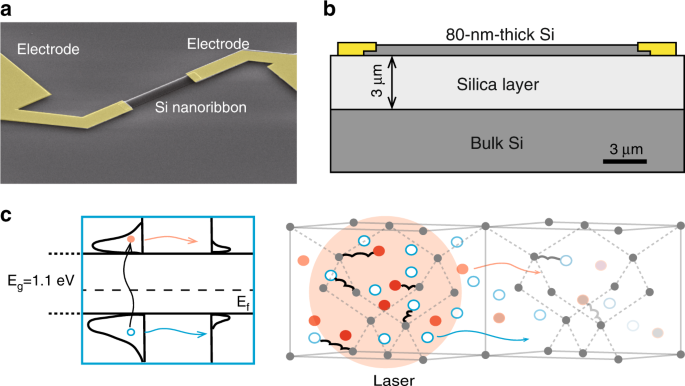
measured electrical sheet conductance). A pseudocolor scanning electron microscopy image and a cross section diagram of the device are shown in Fig. 1a, b, respectively. The fabrication
process is described in the “Materials and methods” section. The Si nanoribbon was 18 μm long, 2.75 μm wide, and 80 nm thick. The length and width of the nanoribbons were chosen based on the
scanning range, step size, and laser spot size in SPCM. Gold (Au) and lightly doped p-type Si formed an ohmic contact, as the work function of Au (−5.1 eV) is lower than the Fermi level of
lightly doped p-type Si (−4.74 eV). Lightly doped p-type Si was used because its Seebeck coefficient showed anomalous behavior with increasing temperature17. The thickness of the Si (80 nm)
was less than the phonon mean free path, estimated to be 300 nm at 300 K18.
a False-color scanning electron microscopy image of the device. b Structural diagram of the device cross section. The length and width of the Si nanoribbon were 18 and 2.75 μm, respectively.
The electrode was Au. c Schematic of the hot carrier generation in the Si band diagram (left) and their dynamics in a Si nanoribbon (right). Electron–hole pairs were generated using laser
irradiation on the left part and diffused from the hot region to the far end. The hollow blue circles and solid red dots represent holes and electrons, respectively. The red and blue lines
represent diffusion of the electrons and holes, respectively. The color intensity of the electrons represents kinetic energy. The large gray solid dots are the projected Si atoms in the
diamond crystal structure.
A one-dimensional transport model of the PTE effect is shown in Fig. 1c. Because the thickness of the Si was much smaller than the optical absorption depth (3.45 μm at a wavelength of 633
nm), the change in the carrier concentration in this direction was negligible. When the 633-nm focused laser irradiated the left end of the Si nanoribbon, many electron–hole pairs were
generated at the irradiated position. The hot carriers were generated within hundreds of femtoseconds of carrier–carrier scattering19. The hot carriers then scattered with the optical
phonons and approached the quasiequilibrium state within hundreds of picoseconds, and the carrier temperature was higher than that of the lattice. For Au/Si ohmic contact PTE effect devices,
the main contribution to the photocurrent is the photogenerated hot carriers diffusing from the excitation (hot) region to the far end, driven by the carrier temperature and concentration
gradient. Because p-type Si was used, the holes contributed more to the thermoelectric process, forming a net current flowing from the excitation region to the far end (j = −σS∇T, where σ is
conductivity, and S is the Seebeck coefficient; S > 0 for p-type Si, because hole diffusion is dominant). The measurable photocurrent/photovoltage of the PTE effect also benefitted from the
high Seebeck coefficient of the lightly doped p-type Si (measured value 9.9 mV K−1). For comparison, a PV effect device was also studied in this work. The open-circuit voltage depends upon
the built-in voltage and how far the Fermi levels must change for the internal diffusion current to exactly balance the photocurrent to give an external zero current. The Fermi energy
difference resulted in an induced electric field that separated the photogenerated electron–hole pairs20. The PV effect is commonly observed in p–n junctions or metal/semiconductor Schottky
junctions. PTE and PV effects could be distinguished by the sign of the open-circuit voltage/short-circuit current from the scanning photovoltage/photocurrent microscopy21. Differentiating
the PTE effect from the PV effect has been reported in black phosphorus16 and MoS222.
The presence of the PTE effect in Si nanoribbon photodetectors was confirmed by the experimental results as follows. First, it was confirmed by SPCM of different electrode contact
devices10,21,23. The key factor affecting the PV and PTE effects was the contact properties of the metal and Si. Possibly owing to the lack of annealing electrodes in the experiment, while
most devices showed ohmic contacts because of the Au/Si contact, some devices showed Schottky contact behavior because of the chromium (Cr)/Si contact. Schottky contact is formed because the
work function of Cr (−4.5 eV) is higher than the Fermi level of lightly doped p-type Si. Thus, it forms a barrier to the holes. The metal–semiconductor contact types for different devices
were confirmed by their measured I–V characteristics. Figure 2a, c shows the I–V curves for two devices having different contacts. The I–V curves were measured under dark conditions over a
voltage range from −2 to 2 V, which was sufficiently broad to verify the electrode contact type. For the sample having Schottky contacts, the I–V curve represented the response of two
back-to-back series diodes, in which the current showed a symmetric reverse-bias-dominated response with external voltage. When the applied voltage was greater than 0.2 V, the gradually
increasing leakage current could have been due to either the additional barrier height reduction upon applied voltage, such as the Schottky effect, or the increased number of thermally
generated minority carriers in the larger depletion region at higher applied voltages24. For the device having ohmic contacts, a linear I–V curve was observed, as shown in Fig. 2c,
indicating that there was no significant band bending effect.
The measured I–V curves of a the Schottky electrode contact device and c the ohmic electrode contact device without light irradiation. b, d The corresponding short-circuit photocurrent, Isc,
scanned in space. The laser wavelength was 633 nm, and the power was 0.18 μW (3.67 W cm−2). The yellow and gray regions correspond to the electrode and Si nanoribbon, respectively.
Figure 2b, d shows the corresponding SPCM results for Schottky and ohmic devices. The short-circuit current, Isc, was measured under ambient conditions without external bias. The laser
wavelength was 633 nm, and the spot diameter was 2.5 μm. For the Cr/Si Schottky contact devices, the maximum value of the photocurrent occurred near the electrode and at the edge of the Si
nanoribbon with a negative photocurrent on the left side of the device and a positive photocurrent on the right side of the device, as shown in Fig. 2b. The direction of the photocurrent
indicated a downward energy band bending in the device. These observations indicate electron–hole separation in the Schottky junction, meaning that the photocurrent was caused by the PV
effect. However, for the ohmic device, the photocurrent scanning result was the opposite of that for the device with the Schottky junction. The reversed sign of the photocurrent can be
attributed to the PTE effect, in which the current direction was determined by the carrier temperature gradient and the majority carrier diffusion. Thus, these results successfully
differentiated the PV effect from the PTE effect for different Schottky/ohmic contacts.
Second, the PTE effect in Si nanoribbon photodetectors was evidenced by the large photovoltage, which would have been impossible from the thermoelectric effect caused by the small increase
in lattice temperature. The increase in lattice temperature in the illuminated Si nanoribbon was estimated by both a COMSOL simulation and the reported photoinduced lattice temperature
increase coefficient. The increase in lattice temperature in the Si nanoribbon in the irradiated region estimated by COMSOL was

:max_bytes(150000):strip_icc():focal(319x0:321x2)/people_social_image-60e0c8af9eb14624a5b55f2c29dbe25b.png)

:max_bytes(150000):strip_icc():focal(656x18:658x20)/mandy-moore-3-257e49bb415c47a9ac42dde58c0ea78a.jpg)


:max_bytes(150000):strip_icc():focal(779x229:781x231)/lord-chamberlain-breaking-want-091922-8ceb88c79fb04ebd8c408021d519cb09.jpg)
