- Select a language for the TTS:
- UK English Female
- UK English Male
- US English Female
- US English Male
- Australian Female
- Australian Male
- Language selected: (auto detect) - EN
Play all audios:
ABSTRACT There are only a handful of scanning techniques that can provide surface topography at nanometre resolution. At the same time, there are no methods that are capable of non-invasive
imaging of the three-dimensional surface topography of a thin free-standing crystalline material. Here we propose a new technique—the divergent beam electron diffraction (DBED) and show that
it can directly image the inhomogeneity in the atomic positions in a crystal. Such inhomogeneities are directly transformed into the intensity contrast in the first-order diffraction spots
of DBED patterns and the intensity contrast linearly depends on the wavelength of the employed probing electrons. Three-dimensional displacement of atoms as small as 1 angstrom can be
detected when imaged with low-energy electrons (50–250 eV). The main advantage of DBED is that it allows visualization of the three-dimensional surface topography and strain distribution at
the nanometre scale in non-scanning mode, from a single shot diffraction experiment. SIMILAR CONTENT BEING VIEWED BY OTHERS IMAGING TWO-DIMENSIONAL GENERALIZED WIGNER CRYSTALS Article 29
September 2021 MAPPING NANOSCALE CARRIER CONFINEMENT IN POLYCRYSTALLINE GRAPHENE BY TERAHERTZ SPECTROSCOPY Article Open access 07 February 2024 STRAIN DISTRIBUTION IN WS2 MONOLAYERS DETECTED
THROUGH POLARIZATION-RESOLVED SECOND HARMONIC GENERATION Article Open access 02 July 2024 INTRODUCTION Measurements of surface topography with atomic resolution is absolutely crucial for
many branches of science, including physics, chemistry and biology. Free-standing graphene, with its intrinsic and extrinsic ripples, offers an ideal test object for any three-dimensional
surface mapping technique. According to the Mermin-Wagner theorem, at any finite temperature two-dimensional materials must exhibit intrinsic corrugations1. Such intrinsic ripples with a
period of about 5–10 nm were predicted for free-standing graphene by Monte Carlo simulations2. In 2007, Meyer _et al_.3,4 performed convergent beam electron diffraction (CBED) imaging of
graphene, observing intensity variations in the first-order diffraction spots. CBED was realized in a conventional TEM where the electron beam spatial coherence was about 10 nm. These
intensity variations were explained by changes in the local orientation of graphene, namely by its deflection within ±2° from the normal to the flat surface3 or by 0.1 rad (ref. 4), which
could be attributed to ripples with the amplitude of 1 nm at 20 nm length. There are a number of techniques that allow surface topography to be measured with nanometre resolution, such as
scanning tunnelling microscopy (STM)5 and atomic force microscopy6. Furthermore, some of them have been applied to image ripples in graphene7. However, it is not possible to call such
techniques completely non-invasive. Graphene has very low bending rigidity, and the probe can affect the ripple distribution. This is, for instance, the case in STM imaging of free-standing
graphene8, where strong interaction between the STM tip and the graphene can even lead to the flipping of ripples9. Also, scanning techniques, because of slow scanning speed, intrinsically
incapable of obtaining temporal dynamics across the studied surface, which is expected for flexural phonon modes10. So far, only the temporal dynamics of a ripple at the fixed tip position11
has been obtained by STM. Thus, there is no technique that allows the three-dimensional surface topography of a thin free-standing crystalline material to be detected in a non-invasive and
non-scanning mode. We propose divergent beam electron diffraction (DBED), which can be realized for thin crystalline samples in transmission mode. DBED allows imaging of a few hundreds nm2
area in a non-invasive and non-scanning mode, such as a single-shot diffraction experiment, and can be applied for the observation of the temporal dynamics of the three-dimensional surface.
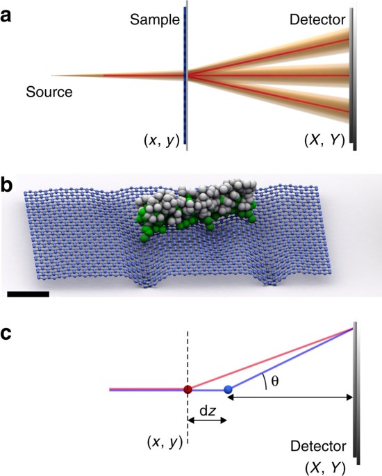
RESULTS CONDITION FOR OBSERVATION OF DBED PATTERNS To understand the formation of the intensity contrast in DBED we consider diffraction of electron wavefront by a periodic lattice of
graphene. When a plane wave scatters off a periodic sample, diffraction peaks are observed in the far-field intensity distribution. Conventionally, the distribution of the intensity in a
diffraction pattern is presented in K-coordinates, where , _λ_ is the wavelength and _ϑ_ is the scattering angle. The positions of the diffraction peaks are determined by fulfilling the
Bragg condition or alternatively by the Ewald’s sphere construction. For a periodic lattice with period _a_, the corresponding reciprocal lattice points are found at _k_=2_π_/_a_ in the
reciprocal space. Whether the corresponding diffraction peaks are observed on a detector or not is determined by the _k_-component range of the imaging system . For example, for graphene,
the six first-order diffraction peaks at _k_1=2_π_/_a_1 are associated with diffraction at crystallographic planes with the period _a_1=2.13 Å. To detect these first-order diffraction peaks
of graphene, the wavelength of the imaging electrons (_λ_), and the maximum acceptance angle of the imaging system (_ϑ_max) must be selected such that : When the incident wave is not a plane
wave, but rather diverges, as in the DBED regime, each diffraction peak turns into a finite-size intensity spot, but the positions of the spots remain the same as the positions of the
diffraction peaks, as illustrated in Fig. 1a. The intensity distribution within one DBED spot reflects the deviation of the atom distribution from the perfect periodic positions. If graphene
is rippled, the carbon atoms deviate from their perfect lattice positions in all three dimensions. Such ripples can be intrinsic, or be caused by, for instance, an adsorbate on the surface
of graphene (Fig. 1b). Two waves scattered off two atoms at different _z_-positions travel across different optical paths to a certain point on a detector, as illustrated in Fig. 1c. The
difference in the optical paths amounts to where d_z_ is the difference in _z_-positions of the atoms, and _θ_ is the scattering angle. The intensity of the formed interference pattern is
proportional to the relative phase shifts between the scattered waves Δ_ϕ_=_k_Δ_s_. For small scattering angles, as for example in the zero-order DBED spot, the phase shift is negligible and
no intensity contrast variations are expected. For higher scattering angles, as in the first-order DBED spot, the phase shift becomes significant, thus leading to noticeable intensity
variations. Therefore, the intensity in the zero-order DBED spot is not sensitive to variations in the _z_-positions of the atoms, whereas the intensity distribution in the higher-order DBED
spots is highly sensitive to the distribution of atomic _z_-positions; see also Supplementary Fig. 1. This holds for any wavelength of the imaging electrons. Although we present
experimental data acquired with low-energy electrons (230 and 360 eV), similar DBED patterns can be acquired with high-energy electrons in a conventional TEM. It must be pointed out that
lower-energy electrons are more sensitive to the distribution of _z_-positions of atoms in a two-dimensional material. For example, for graphene, a ripple of height _h_ will cause intensity
variations in the first-order DBED spot because of a superposition of the scattered waves with the phase shift Thus the phase shift, and therefore the contrast of the formed interference
pattern, depends on the wavelength of the probing wave and decreases as the energy of the probing waves increases. For low-energy electrons, even a small height _h_ of the ripples will cause
a significant phase shift and noticeable interference pattern in a first-order DBED spot. For example, a ripple with _h_=1 Å, when imaged with electrons of 230 eV kinetic energy, will cause
a phase shift of about Δ_ϕ_=0.5 radian in the first-order DBED spot. Another advantage of using low-energy electrons is their relatively low radiation damage12. EXPERIMENTAL REALIZATION OF
DBED Recently, it was reported that electron point projection microscopy (PPM), which is also a Gabor-type in-line holography13,14,15,16,17, has been applied to image graphene. In certain
experimental geometrical arrangements PPM resulted in a very bright central spot and six first-order diffraction spots18. However, no quantitative explanation for intensity variations within
the diffraction spots was provided. Figure 2a shows the experimental arrangement of the low-energy electron point projection microscope used in this work, which has been described
elsewhere18. The electron beam is field emitted from a single-atom tip (SAT)19,20, in this case we used an iridium-covered W(111) SAT (refs 21, 22). This type of SAT has been demonstrated to
provide high brightness and fully spatially coherent electron beams21,22 with Gaussian distributed intensity profiles and a full divergence angle of 2–6°. We studied free-standing monolayer
graphene stretched over a hole in a gold-coated Si3N4 membrane, (for preparation procedure see ref. 18). When the tip is positioned at a short distance (microns or smaller) in front of the
sample, the transmitted electron beam forms a magnified projection image of the illuminated sample (zero-order spot pattern) at the detector, as shown in Fig. 2b. The magnification is given
by _M_=_D_/_d_, where _d_ is the source-to-sample distance and _D_ is the source-to-detector distance. A DBED pattern is observed when parameters of the experimental setup satisfy equation
(1). The size of the zero- and first-order DBED spots is given by the size of the imaged area (limited either by the size of the probing beam or by the size of the sample supporting
aperture) multiplied by the magnification _M_. Figure 2 shows DBED pattern recorded at _t_=0, 200 and 500 s. Figure 2c presents the central spot recorded at _t_=0, 200 and 500 s and Fig. 2d
shows the sample distribution obtained by reconstruction of the central spot at _t_=0 s. The dark distributions on the right and left edges in the zero-order DBED spots can be associated
with the aggregation of adsorbates on graphene, which are non-transparent for the electron beam. The centre region in the zero-order DBED spot is formed by the electron wave transmitted
mainly through a clean graphene region with only one or two darker or brighter spots corresponding to small individual adsorbates23. The dark distributions associated with adsorbate
aggregates remain visible in the first-order DBED spots. However, in addition, bright and dark stripes are evident in the region between the dark distributions. As demonstrated above, the
first-order DBED spots (Fig. 2e–g) exhibit intensity contrast variations that are not observed in the corresponding area of the zero-order DBED spot, which agrees well with the
aforementioned explanations that waves scattered off atoms positioned at different _z_-positions, contribute to the contrast formation at high scattering angles. Also, it should be noted
that the first-order DBED spots have slightly different intensity distributions between themselves. From the data presented in Fig. 2e–g, it can be seen that the intensity distribution
within the first-order DBED spots also varies in time, probably due to changes in the distribution of the adsorbates. SIMULATED DBED PATTERNS To characterize the observed ripples
quantitatively, we performed numerical simulations of DBED patterns. The diffracted wavefront at the detector is simulated using the following distribution: where _t_(_x_, _y_, _z_) is the
transmission function in the object domain, (_x_, _y_, _z_) are the coordinates in the sample domain and (_X_, _Y_) are the coordinates in the detector plane. _t_(_x_, _y_, _z_) includes the
aperture distribution _A_(_X_, _Y_) and the carbon atom distribution in graphene _G_0(_x__i_, _y__i_, _z__i_), where _G_0(_x__i_, _y__i_, _z__i_) is 1 at the position (_x__i_, _y__i_,
_z__i_) of carbon atom _i_ and 0 elsewhere. Details of the simulation are provided in the Methods. Note that the simulations were performed assuming a monochromatic spatially coherent
electron source. No other approximations and no fast Fourier transforms are used in this simulation. The following device configurations were simulated and are shown in Figs 3 and 4: clean
graphene (Fig. 3a–b), graphene with a single adsorbate (Fig. 3c–f), graphene with an out-of-plane ripple (Fig. 4a–f) and graphene with an in-plane ripple (Fig. 4g–i). In all simulated DBED
patterns, the intensity of the zero-order DBED spot is about 50 times higher than that of the first-order DBED spots, which agrees with the experimental observations. The first-order DBED
spots appear to be distorted because of the geometrical conditions selected in the simulations: plane detector and relatively short distance between the source and the sample. A simulated
DBED pattern of perfectly planar clean graphene stretched over an aperture, as illustrated in Fig. 3a, is shown in Fig. 3b. A simulated DBED pattern of graphene with an opaque adsorbate in
the form of the letter Ψ on its surface (as illustrated in Fig. 3c–d), is shown in Fig. 3e. From Fig. 3e,f, it can be seen that the presence of an adsorbate changes the contrast of the
zero-order DBED spot, which appears as an in-line hologram of the adsorbate. The simulated first-order DBED spots exhibit similar contrast variations as the zero-order DBED spot, though less
pronounced. Thus, the presence of an adsorbate creates almost the same intensity distribution in all DBED spots. In the real experimental situation an adsorbate on graphene can cause a
certain amount of strain and hence additional rippling in graphene. We simulated two kinds of ripples: out-of-plane and in-plane. In the simulations, the carbon atoms are shifted from their
perfect lattice positions _G_0(_x__i_, _y__i_, _z__i_) in the graphene plane. Each ripple is described by a Gaussian distribution with amplitude _h_ and s.d. _σ_. The results of the
simulations are shown in Fig. 4. Two simulated out-of-plane ripples are sketched in Fig. 4a,d: in the negative _z_-direction (towards the electron source) and in the positive _z_-direction
(away from the electron source). The parameters of the ripples are _h_=3 Å and _σ_=1.5 nm. The corresponding simulated DBED patterns are shown in Fig. 4b,e, and the magnified first-order
DBED spots are shown in Fig. 4c,f, respectively. From Fig. 4b,e it can be seen that there is no intensity variations within the zero-order DBED spot, which is similar to the behaviour of the
zero-order DBED spot intensity of a clean graphene region in experimental and simulated DBED patterns: Figs 2c and 3b, respectively. At the same time, all the first-order DBED spots
demonstrate very similar intensity variations that resemble the original ripple distribution. Such resemblance can be explained by considering the ripple as a phase-shifting object that
changes the phase of the incident wave by Δ_ϕ_(_x_, _y_). It has been shown that the phase change introduced to the incident wave in the object domain is preserved while the wave propagates
toward the detector24. Within the approximation of a weak phase-shifting object e_i_Δ_ϕ_(_x_,_y_)≈1+_i_Δ_ϕ_(_x_, _y_). The introduced phase change is transformed into intensity contrast at
the detector as |Δ_ϕ_(_X_, _Y_)|2, as explained in Supplementary Note 1. For a ripple of height _h_, the expected intensity distribution is given by . From these simulations, one can
conclude that the three-dimensional form of a ripple can be directly visualized from the intensity distribution in the first-order DBED spot: a ripple towards the source results in a darker
intensity distribution (Fig. 4a–c), while a ripple towards the detector results in a brighter intensity distribution (Fig. 4d–f). For example, most of the ripples in the experimental
distributions shown in Fig. 2 are out-of-plane ripples towards the detector. The intensity profiles of the DBED patterns of the out-of-plane ripples of amplitude 1 and 2 Å are provided in
Supplementary Fig. 2, demonstrating that ripples of 1 Å are already sufficiently strong to cause noticeable intensity variations in the DBED pattern. In the simulation of an in-plane ripple,
sketched in Fig. 4g, the positions of carbon atoms are shifted laterally in the (_x_, _y_)-planes in the form of a Gaussian-distributed profile with parameters _h_=1 Å and _σ_=5 nm. The
corresponding DBED pattern is shown in Fig. 4h, and the magnified first-order DBED spots are shown in Fig. 4i. Also, for this type of ripple the intensity of the zero-order DBED spot does
not show any variations, similar to the experimental and simulated DBED patterns shown in Figs 2c and 3b, respectively. The first-order DBED spots show pronounced intensity variations, which
only slightly resemble the original ripple distributions. Unlike in the case of the out-of-plane ripples, here the intensity distributions within different first-order DBED spots are very
different from each other. A similar effect is observed in the experimental images. This means that in-plane ripples also contribute to the contrast formation in the first-order DBED spots
in the experimental images. An intensity profile through one of the first-order DBED spots in the experimental data shown in Fig. 2e was fitted with two profiles of simulated DBED patterns
of two out-of-plane ripples. Good matching between the distributions of the simulated and experimentally acquired intensity peaks was observed when the ripples were set to have height _h_=3
Å and standard deviation of _σ_=5 nm and _σ_=3 nm; see Fig. 4j. Experimental parameters such as distances and energies influence the intensity contrast on the detector. The same ripple can
produce different intensity contrast on a detector when, for example, the source-to-sample distance is varied; see the additional simulations provided in Supplementary Fig. 2. DISCUSSION To
summarize, we showed that in DBED patterns the contribution from the adsorbates and three-dimensional distribution of ripples in graphene can be separated by comparing the intensity in the
zero- and the first-order DBED spots. DBED imaging allows direct visualization of the distribution of the ripples in graphene, and thus may provide accurate mapping of the three-dimensional
topography of free-standing graphene. The intensity contrast within the first-order DBED spots linearly depends on the wavelength of the probing electrons. Thus, low-energy electrons are
highly sensitive to inhomogenities in the spatial distribution of atoms. When imaged with low-energy electrons, the ripples of amplitude 1 Å are sufficiently strong to cause noticeable
intensity variations in the first-order diffraction spots of a DBED pattern. Thus, very weak ripples associated with strain caused by adsorbates on the graphene surface can be directly
visualized and studied by DBED. In the experimental images, we observe ripples mainly formed between adsorbates, as though the adsorbates wrinkle the graphene surface around themselves. We
also experimentally observed that the distribution of ripples, and, hence, the strain distribution, varies over time. The out-of-plane and in-plane ripples are distinguishable by their
appearance in the DBED patterns. Out-of-plane ripples produce similar intensity distributions between all the first-order DBED spots, whereas the in-plane ripples produce different intensity
distributions for different first-order DBED spots. From comparison of the experimental results with the simulations, we conclude that the graphene surface is deformed mainly by
out-of-plane ripples with a small contribution from the in-plane ripples. From the intensity of the ripple (darker or brighter), its direction can be estimated. In both simulations and
experiments, the six first-order DBED spots exhibit slightly different distributions of intensity, which suggests that each DBED spot carries information about the three-dimensional surface
illuminated at a slightly different angle. Thus, it should be possible to reconstruct a three-dimensional distribution of graphene surface directly from its DBED pattern. This means that
DBED provides a unique tool that allows the three-dimensional topography and thus the three-dimensional strain distribution to be studied at the nanometre scale. Although we have
demonstrated DBED with low-energy electrons, DBED can be also realized with high-energy electrons in conventional TEM setups. METHODS LOW-ENERGY DBED EXPERIMENTAL ARRANGEMENT The microscope
is housed in an ultra-high vacuum chamber. A SAT is mounted on a three-axis piezo-driven positioner (Unisoku, Japan) with a 5 mm travelling range in each direction. The detector consists of
a micro-channel plate (Hamamatsu F2226-24PGFX, diameter=77 mm) and a phosphorous screen assembly. The detector is mounted on a rail and can be moved along the beam direction. A camera (Andor
Neo 5.5 sCMOS, 16-bit, 2,560 × 2,160 pixels) adapted with a camera head (Nikon AF Micro-Nikkor 60 mm f/2.8 D) is placed behind the screen outside the ultra-high vacuum chamber to record the
images on the screen. The whole system was kept at room temperature during electron emission, and the base pressure of the chamber is around 1 × 10⁻¹⁰ Torr. SIMULATION PROCEDURE _L_(…)
denotes the operator of forward propagation as described in the main text by equation (4). In the simulation, the following steps are carried out: * 1 _U_1(_X_, _Y_)=_L_(_A_(_x_, _y_)) is
simulated, where _A_(_x_, _y_) is the distribution of the aperture over which graphene is supported. _A_(_x_, _y_) is a round aperture, with transmission equal to 1 inside the aperture and 0
outside the aperture; on the edges of the aperture the transmission smoothly changes from 1 to 0 by applying a cosine-window apodization function25. * 2 _U_2(_X_, _Y_)=_L_(_G_(_x__i_,
_y__i_))=_L_(_A_(_x_, _y_)_G_0(_x__i_, _y__i_, _z__i_)) is simulated, where _G_0(_x__i_, _y__i_, _z__i_) is 1 at the position (_x__i_, _y__i_, _z__i_) of carbon atom _i_ and 0 elsewhere.
_G_(_x__i_,_y__i_,_z__i_)=_A_(_x_,_y_)_G_0(_x_,_y_,_z_) is the distribution of the carbon atoms within the aperture. In our simulations, the carbon atoms in graphene are represented by their
coordinates, not as pixels. For each carbon atom within the aperture, the scattered wave is simulated at the detector plane. These waves are then added together giving the total scattered
wave. * 3 The intensity distribution at the screen is simulated as _I_(_X_, _Y_)=|_U_1(_X_, _Y_)−_U_2(_X_, _Y_)|2. Simulation of graphene with adsorbate: In step (1) of the simulation, the
adsorbate distribution is included in _A_(_x_, _y_), and in step (2) the carbon atoms that are at the same position as the adsorbate are excluded from the distribution _G_(_x_, _y_, _z_).
Simulation of an out-of-plane ripple: The positions of carbon atoms are shifted along the _z_-direction in the form of a ripple; the distribution of carbon atoms’ coordinates _G_0(_x_, _y_,
_z_) is accordingly modified. Simulation of an in-plane ripple: The positions of carbon atoms are shifted laterally in the (_x_,_y_)-plane in the form of a ripple; and the distribution
_G_0(_x_,_y_,_z_) is accordingly modified. DATA AVAILABILITY All relevant data are available from the authors. ADDITIONAL INFORMATION HOW TO CITE THIS ARTICLE: Latychevskaia, T. _et al_.
Three-dimensional surface topography of graphene by divergent beam electron diffraction. _Nat. Commun._ 8, 14440 doi: 10.1038/ncomms14440 (2017). PUBLISHER’S NOTE: Springer Nature remains
neutral with regard to jurisdictional claims in published maps and institutional affiliations. REFERENCES * Mermin, N. D. Crystalline order in two dimensions. _Phys. Rev._ 176, 250–254
(1968). Article ADS Google Scholar * Fasolino, A., Los, J. H. & Katsnelson, M. I. Intrinsic ripples in graphene. _Nat. Mater._ 6, 858–861 (2007). Article CAS ADS Google Scholar *
Meyer, J. C. et al. On the roughness of single- and bi-layer graphene membranes. _Solid State Commun._ 143, 101–109 (2007). Article CAS ADS Google Scholar * Meyer, J. C. et al. The
structure of suspended graphene sheets. _Nature_ 446, 60–63 (2007). Article CAS ADS Google Scholar * Binnig, G. & Rohrer, H. Scanning tunneling microscopy. _IBM J. Res. Dev._ 30,
355–369 (1986). CAS Google Scholar * Binnig, G., Quate, C. F. & Gerber, C. Atomic force microscope. _Phys. Rev. Lett._ 56, 930–933 (1986). Article CAS ADS Google Scholar *
Geringer, V. et al. Intrinsic and extrinsic corrugation of monolayer graphene deposited on SiO2 . _Phys. Rev. Lett._ 102, 076102 (2009). Article CAS ADS Google Scholar * Zan, R. et al.
Scanning tunnelling microscopy of suspended graphene. _Nanoscale_ 4, 3065–3068 (2012). Article CAS ADS Google Scholar * Breitwieser, R. et al. Flipping nanoscale ripples of free-standing
graphene using a scanning tunneling microscope tip. _Carbon_ 77, 236–243 (2014). Article CAS Google Scholar * Smolyanitsky, A. & Tewary, V. K. Manipulation of graphene’s dynamic
ripples by local harmonic out-of-plane excitation. _Nanotechnology_ 24, 055701 (2013). Article CAS ADS Google Scholar * Xu, P. et al. Unusual ultra-low-frequency fluctuations in
freestanding graphene. _Nat. Commun._ 5, 3720 (2014). Article CAS Google Scholar * Germann, M., Latychevskaia, T., Escher, C. & Fink, H.-W. Nondestructive imaging of individual
biomolecules. _Phys. Rev. Lett._ 104, 095501 (2010). Article ADS Google Scholar * Gabor, D. A new microscopic principle. _Nature_ 161, 777–778 (1948). Article CAS ADS Google Scholar *
Gabor, D. Microscopy by reconstructed wave-fronts. _Proc. R. Soc. Lond. A_ 197, 454–487 (1949). Article ADS Google Scholar * Stocker, W., Fink, H.-W. & Morin, R. Low-energy electron
and ion projection microscopy. _Ultramicroscopy_ 31, 379–384 (1989). Article Google Scholar * Stocker, W., Fink, H.-W. & Morin, R. Low-energy electron projection microscopy. _J. Phys._
50, C8519–C8521 (1989). Google Scholar * Fink, H.-W., Stocker, W. & Schmid, H. Holography with low-energy electrons. _Phys. Rev. Lett._ 65, 1204–1206 (1990). Article CAS ADS Google
Scholar * Chang, W.-T. et al. Low-voltage coherent electron imaging based on a single-atom electron source. Preprint at _arXiv_, 1512.08371 (2015). * Fink, H.-W. Mono-atomic tips for
scanning tunneling microscopy. _IBM J. Res. Dev._ 30, 460–465 (1986). Article CAS Google Scholar * Fink, H.-W. Point-source for ions and electrons. _Phys. Scripta_ 38, 260–263 (1988).
Article CAS ADS Google Scholar * Kuo, H. S. et al. Preparation and characterization of single-atom tips. _Nano Lett._ 4, 2379–2382 (2004). Article CAS ADS Google Scholar * Chang, C.
C., Kuo, H. S., Hwang, I. S. & Tsong, T. T. A fully coherent electron beam from a noble-metal covered W(111) single-atom emitter. _Nanotechnology_ 20, 115401 (2009). Article ADS Google
Scholar * Latychevskaia, T., Wicki, F., Longchamp, J.-N., Escher, C. & Fink, H.-W. Direct observation of individual charges and their dynamics on graphene by low-energy electron
holography. _Nano Lett._ 16, 5469–5474 (2016). Article CAS ADS Google Scholar * Latychevskaia, T. & Fink, H.-W. Reconstruction of purely absorbing, absorbing and phase-shifting, and
strong phase-shifting objects from their single-shot in-line holograms. _Appl. Opt._ 54, 3925–3932 (2015). Article ADS Google Scholar * Latychevskaia, T. & Fink, H.-W. Practical
algorithms for simulation and reconstruction of digital in-line holograms. _Appl. Opt._ 54, 2424–2434 (2015). Article ADS Google Scholar Download references ACKNOWLEDGEMENTS This research
is supported by Academia Sinica of R.O.C. (AS-102-TP-A01). AUTHOR INFORMATION Author notes * [email protected] AUTHORS AND AFFILIATIONS * Physics Department of the University of
Zurich, Winterthurerstrasse 190, Zürich, CH-8057, Switzerland Tatiana Latychevskaia * Institute of Physics, Academia Sinica, Nankang, 115, Taipei, Taiwan Wei-Hao Hsu, Wei-Tse Chang,
Chun-Yueh Lin & Ing-Shouh Hwang * Department of Materials Science and Engineering, National Tsing Hua University, Hsinchu, 300, Taiwan Wei-Hao Hsu & Ing-Shouh Hwang Authors * Tatiana
Latychevskaia View author publications You can also search for this author inPubMed Google Scholar * Wei-Hao Hsu View author publications You can also search for this author inPubMed Google
Scholar * Wei-Tse Chang View author publications You can also search for this author inPubMed Google Scholar * Chun-Yueh Lin View author publications You can also search for this author
inPubMed Google Scholar * Ing-Shouh Hwang View author publications You can also search for this author inPubMed Google Scholar CONTRIBUTIONS I.-S.H. initiated the project of low-energy
electron imaging; W.-H.H., W.-T.C. and C.-Y.L. designed and performed experiments; W.-H.H. acquired the DBED patterns; I.-S.H. contributed to writing the manuscript; W.-H.H., W.-T.C.,
C.-Y.L. and I.-S.H. participated in discussions. T.L. proposed explanation of the observed experimental effects, developed the theory, made the simulations, analysed the experimental data
and wrote the manuscript. CORRESPONDING AUTHORS Correspondence to Tatiana Latychevskaia or Ing-Shouh Hwang. ETHICS DECLARATIONS COMPETING INTERESTS The authors declare no competing financial
interests. SUPPLEMENTARY INFORMATION SUPPLEMENTARY INFORMATION Supplementary Figures and Supplementary Note. (PDF 318 kb) RIGHTS AND PERMISSIONS This work is licensed under a Creative
Commons Attribution 4.0 International License. The images or other third party material in this article are included in the article’s Creative Commons license, unless indicated otherwise in
the credit line; if the material is not included under the Creative Commons license, users will need to obtain permission from the license holder to reproduce the material. To view a copy of
this license, visit http://creativecommons.org/licenses/by/4.0/ Reprints and permissions ABOUT THIS ARTICLE CITE THIS ARTICLE Latychevskaia, T., Hsu, WH., Chang, WT. _et al._
Three-dimensional surface topography of graphene by divergent beam electron diffraction. _Nat Commun_ 8, 14440 (2017). https://doi.org/10.1038/ncomms14440 Download citation * Received: 20
September 2016 * Accepted: 30 December 2016 * Published: 14 February 2017 * DOI: https://doi.org/10.1038/ncomms14440 SHARE THIS ARTICLE Anyone you share the following link with will be able
to read this content: Get shareable link Sorry, a shareable link is not currently available for this article. Copy to clipboard Provided by the Springer Nature SharedIt content-sharing
initiative