- Select a language for the TTS:
- UK English Female
- UK English Male
- US English Female
- US English Male
- Australian Female
- Australian Male
- Language selected: (auto detect) - EN
Play all audios:
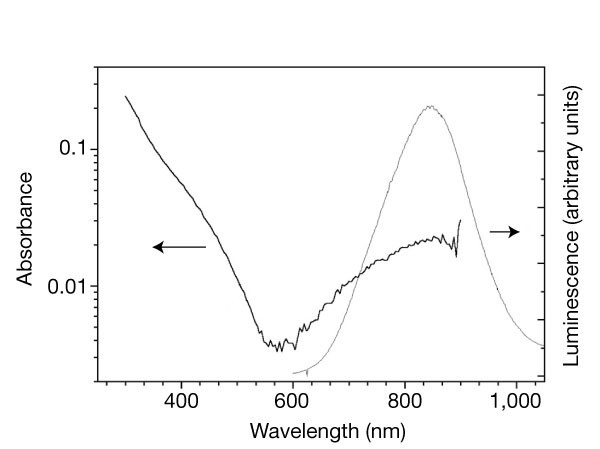
ABSTRACT Adding optical functionality to a silicon microelectronic chip is one of the most challenging problems of materials research. Silicon is an indirect-bandgap semiconductor and so is
an inefficient emitter of light. For this reason, integration of optically functional elements with silicon microelectronic circuitry has largely been achieved through the use of
direct-bandgap compound semiconductors. For optoelectronic applications, the key device is the light source—a laser. Compound semiconductor lasers exploit low-dimensional electronic systems,
such as quantum wells and quantum dots, as the active optical amplifying medium. Here we demonstrate that light amplification is possible using silicon itself, in the form of quantum dots
dispersed in a silicon dioxide matrix. Net optical gain is seen in both waveguide and transmission configurations, with the material gain being of the same order as that of direct-bandgap
quantum dots. We explain the observations using a model based on population inversion of radiative states associated with the Si/SiO2 interface. These findings open a route to the
fabrication of a silicon laser. Access through your institution Buy or subscribe This is a preview of subscription content, access via your institution ACCESS OPTIONS Access through your
institution Subscribe to this journal Receive 51 print issues and online access $199.00 per year only $3.90 per issue Learn more Buy this article * Purchase on SpringerLink * Instant access
to full article PDF Buy now Prices may be subject to local taxes which are calculated during checkout ADDITIONAL ACCESS OPTIONS: * Log in * Learn about institutional subscriptions * Read our
FAQs * Contact customer support SIMILAR CONTENT BEING VIEWED BY OTHERS ALL-SILICON QUANTUM LIGHT SOURCE BY EMBEDDING AN ATOMIC EMISSIVE CENTER IN A NANOPHOTONIC CAVITY Article Open access
07 June 2023 HIGHLY EFFICIENT NONLINEAR OPTICAL EMISSION FROM A SUBWAVELENGTH CRYSTALLINE SILICON CUBOID MEDIATED BY SUPERCAVITY MODE Article Open access 18 May 2022 PROGRAMMABLE QUANTUM
EMITTER FORMATION IN SILICON Article Open access 27 May 2024 REFERENCES * Canham, L. T. Silicon quantum wire array fabrication by electrochemical and chemical dissolution of wafers. _Appl.
Phys. Lett._ 57, 1045– 1048 (1990). Article ADS Google Scholar * Cullis, A. G. & Canham, L. T. Visible light emission due to quantum size effects in highly porous crystalline silicon.
_Nature _ 353, 335–338 ( 1991). Article ADS CAS Google Scholar * Wilson, W. L., Szajowski, P. F. & Brus, L. E. Quantum confinement in size-selected surface-oxidised silicon
nanocrystals. _Science_ 262, 1242– 1244 (1993). Article ADS CAS Google Scholar * Lu, Z. H., Lockwood, D. J. & Baribeau, J.-M. Quantum confinement and light emission in SiO 2/Si
superlattices. _Nature_ 378, 258 –260 (1995). Article ADS CAS Google Scholar * Hirschman, K. D., Tsybeskov, L., Duttagupta, S. P. & Fauchet, P. M. Silicon-based light emitting
devices integrated into microelectronic circuits. _Nature_ 384, 338–340 (1996). Article ADS CAS Google Scholar * Franzò, G., Priolo, F., Coffa, S., Polman, A. & Carnera, A. Room
temperature electroluminescence from Er doped crystalline silicon. _Appl. Phys. Lett._ 64, 2235– 2237 (1994). Article ADS Google Scholar * Leong, D., Harry, M., Reeson, K. J. &
Homewood, K. P. A silicon/iron disilicide light-emitting diode operating at a wavelength of 1.5 µm. _Nature_ 387, 686–688 (1997). Article ADS CAS Google Scholar * Nassiopoulos, A. G.,
Grigoropoulos, S. & Papadimitriou, D. Electroluminescent device based on silicon nanopillars. _Appl. Phys. Lett._ 69, 2267– 2269 (1996). Article ADS CAS Google Scholar * Bisi, O.,
Ossicini, S. & Pavesi, L. Porous silicon: a quantum sponge structure for silicon based optoelectronics. _Surf. Sci. Rep._ 38, 1–126 (2000). Article ADS CAS Google Scholar * Wolkin,
M. V., Jorne, J., Fauchet, P. M., Allan, G. & Delerue, C. Electronic states and luminescence in porous silicon quantum dots: the role of oxygen. _Phys. Rev. Lett._ 82, 197–200 ( 1999).
Article ADS CAS Google Scholar * Miller, D. A. Silicon sees the light. _Nature_ 378, 238 (1995). Article ADS CAS Google Scholar * Iyer, S. S. & Xie, Y.-H. Light emission from
silicon. _ Science_ 260, 40–46 ( 1993). Article ADS CAS Google Scholar * Silicon based optoelectronics. _Mater. Res. Bull._ 23(4), (1998). * Fauchet, P. M. The integration of nanoscale
porous silicon light emitters: materials science, properties and integration with electronic circuitry. _J. Lumin. _ 80, 53–64 ( 1999). Article Google Scholar * Yariv, A. _ Quantum
Electronics_ 2nd edn (Wiley & Sons, New York, 1974). Google Scholar * Canham, L. T. in _ Frontiers of Nano-Optoelectronic Systems_ (eds Pavesi, L. & Buzaneva, E.) 85–98 (Kluwer
Academic, Dordrecht, 2000). Book Google Scholar * Iacona, F., Franzò, G. & Spinella, C. Correlation between luminescence and structural properties of Si nanocrystals. _J. Appl. Phys._
87, 1295 –1303 (2000). Article ADS CAS Google Scholar * Kovalev, D., Heckler, H., Polisski, G. & Koch, F. Optical properties of Si nanocrystals. _Phys. Status Solidi_ 251, 871–930
(1999). Article Google Scholar * Kanemitsu, Y. & Okamoto, S. Quantum confinement and interface effects on photoluminescence from silicon single quantum wells. _ Solid State Commun._
103, 573–576 (1997). Article ADS Google Scholar * Kanemitsu, Y. & Okamoto, S. Phonon structures and Stokes shift in resonantly excited luminescence of silicon nanocrystals. _Phys.
Rev. B_ 58, 9652–9655 ( 1998). Article ADS CAS Google Scholar * Degoli, E. & Ossicini, S. Quantum confined and interface states related visible luminescence in Si/SiO2 superlattices.
_ Surf. Sci._ (in the press). * Klimov, V. I., Schwarz, Ch., McBranch, D. W. & White, C. W. Initial carrier relaxation dynamics in ion-implanted Si nanocrystals: femtosecond transient
absorption study. _Appl. Phys. Lett._ 73, 2603–2605 (1998). Article ADS CAS Google Scholar * Linnros, J., Galeckas, A., Lalic, N. & Grivickas, V. Time-resolved photoluminescence
characterisation of nm-sized silicon nanocrystallites in SiO2. _Thin Solid Films_ 297, 167 –170 (1997). Article ADS CAS Google Scholar * Shaklee, K. L., Nahaory, R. E. & Leheny, R.
F. Optical gain in semiconductors. _J. Lumin. _ 7, 284–309 ( 1973). Article CAS Google Scholar * Kirstaedter, N. _ et al_. Gain and differential gain of single layer InAs/GaAs quantum dot
injection lasers. _Appl. Phys. Lett._ 69, 1226–1228 (1996). Article ADS CAS Google Scholar * Lingk, C. _et al_. Dynamics of amplified spontaneous emission in InAs/GaAs quantum dots.
_Appl. Phys. Lett._ 76, 3507– 3509 (2000). Article ADS CAS Google Scholar * Blood, P. On the dimensionality of optical absorption, gain and recombination in quantum-confined structures.
_IEEE J. Quantum Electron._ 36, 354–362 (2000). Article ADS CAS Google Scholar * Kovalev, D. _ et al_. Optical absorption cross sections of Si nanocrystals. _ Phys. Rev. B_ 61, 4485–4487
(2000). Article ADS CAS Google Scholar * von Behren, J., Kostoulas, Y., Ucer, K. B. & Fauchet, P. M. The femtosecond optical response of porous, amorphous and crystalline silicon.
_J. Non-Cryst. Solids_ 198–200, 957 –960 (1996). Article ADS Google Scholar * Jordan, V. Gain measurements of semiconductor laser diodes: requirements for wavelength resolution and
sensitivity to noise. _IEE Proc. Optoelectron._ 141, 13–15 (1994). Article Google Scholar * Hvam, J. M. Direct recording of optical gain spectra from ZnO. _J. Appl. Phys. _ 49, 3124–3126 (
1978). Article ADS CAS Google Scholar Download references ACKNOWLEDGEMENTS This work has been supported by the National Institute for the Physics of the Matter (INFM) through the LUNA
project and the advanced research project RAMSES. AUTHOR INFORMATION AUTHORS AND AFFILIATIONS * INFM & Dipartimento di Fisica Università di Trento, Via Sommarive 14, Povo, 38050, Italy
L. Pavesi, L. Dal Negro & C. Mazzoleni * INFM & Dipartimento di Fisica e Astronomia, Università di Catania, Corso Italia 57 , Catania, 95129, Italy G. Franzò & F. Priolo Authors
* L. Pavesi View author publications You can also search for this author inPubMed Google Scholar * L. Dal Negro View author publications You can also search for this author inPubMed Google
Scholar * C. Mazzoleni View author publications You can also search for this author inPubMed Google Scholar * G. Franzò View author publications You can also search for this author inPubMed
Google Scholar * F. Priolo View author publications You can also search for this author inPubMed Google Scholar CORRESPONDING AUTHOR Correspondence to L. Pavesi. SUPPLEMENTARY INFORMATION
SUPPLEMENTARY FIGURES 1–3. RIGHTS AND PERMISSIONS Reprints and permissions ABOUT THIS ARTICLE CITE THIS ARTICLE Pavesi, L., Dal Negro, L., Mazzoleni, C. _et al._ Optical gain in silicon
nanocrystals. _Nature_ 408, 440–444 (2000). https://doi.org/10.1038/35044012 Download citation * Received: 08 June 2000 * Accepted: 24 October 2000 * Issue Date: 23 November 2000 * DOI:
https://doi.org/10.1038/35044012 SHARE THIS ARTICLE Anyone you share the following link with will be able to read this content: Get shareable link Sorry, a shareable link is not currently
available for this article. Copy to clipboard Provided by the Springer Nature SharedIt content-sharing initiative

:max_bytes(150000):strip_icc():focal(738x236:740x238)/david-beckham-fallen-tree-010423-1-7c60134c3e984fd1a19f9c4f29e00721.jpg)


:max_bytes(150000):strip_icc():focal(999x0:1001x2)/gettyimages-1161226549-2000-fcbe9aff7d6a4fcca69120cfe6ca530c.jpg)