Play all audios:
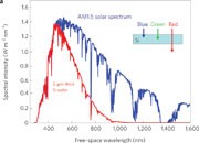
_Nature Materials_ 9, 205–213 (2010); published online 19 February 2010; corrected online 1 September 2010. In Fig. 1a of the version of this Review originally published, the graph labelled
'2-μm-thick Si wafer' is that for a 10-μm-thick Si wafer. The corrected figure is shown below. The original figure caption and descriptions in the text are correct. The figure has
been corrected in the HTML and PDF versions of this Review. Authors * Harry A. Atwater View author publications You can also search for this author inPubMed Google Scholar * Albert Polman
View author publications You can also search for this author inPubMed Google Scholar ADDITIONAL INFORMATION The online version of the original article can be found at 10.1038/nmat2629 RIGHTS
AND PERMISSIONS Reprints and permissions ABOUT THIS ARTICLE CITE THIS ARTICLE Atwater, H., Polman, A. Erratum: Plasmonics for improved photovoltaic devices. _Nature Mater_ 9, 865 (2010).
https://doi.org/10.1038/nmat2866 Download citation * Published: 23 September 2010 * Issue Date: October 2010 * DOI: https://doi.org/10.1038/nmat2866 SHARE THIS ARTICLE Anyone you share the
following link with will be able to read this content: Get shareable link Sorry, a shareable link is not currently available for this article. Copy to clipboard Provided by the Springer
Nature SharedIt content-sharing initiative